Van der Waals Materials for Applications in Nanophotonics
Panaiot G. Zoteva∗, Yue Wangb, Daniel Andres-Penaresc, Toby Severs Millarda, Sam Randersona, Xuerong Hua, Luca Sortinod, Charalambos Loucaa, Mauro Brotons-Gisbertc, Tahiyat Huqe, Stefano Vezzolie, Riccardo Sapienzae, Thomas F. Kraussb, Brian D. Gerardotc, Alexander I. Tartakovskiia∗∗
aDepartment of Physics and Astronomy, University of Sheffield, Sheffield, S3 7RH, UK
bSchool of Physics, Engineering and Technology, University of York, York, YO10 5DD, UK
cSchool of Engineering and Physical Sciences, Heriot-Watt University, Edinburgh, EH14 4AS, UK
dChair in Hybrid Nanosystems, Nanoinstitute Munich, Faculty of Physics, Ludwig-Maximilians-Universität, 80539, Munich, Germany
eThe Blackett Laboratory, Department of Physics, Imperial College London, London, SW7 2BW, UK
∗p.zotev@sheffield.ac.uk ∗∗a.tartakovskii@sheffield.ac.uk
Numerous optical phenomena and applications have been enabled by nanophotonic structures. Their current fabrication from high refractive index dielectrics, such as silicon or gallium phosphide, pose restricting fabrication challenges, while metals, relying on plasmons and thus exhibiting high ohmic losses, limit the achievable applications. Here, we present an emerging class of layered so-called van der Waals (vdW) crystals as a viable nanophotonics platform. We extract the dielectric response of 11 mechanically exfoliated thin-film (20-200 nm) van der Waals crystals, revealing high refractive indices up to n = 5, pronounced birefringence up to n = 3, sharp absorption resonances, and a range of transparency windows from ultraviolet to near-infrared. We then fabricate nanoantennas on SiO2 and gold utilizing the compatibility of vdW thin films with a variety of substrates. We observe pronounced Mie resonances due to the high refractive index contrast on SiO2 leading to a strong exciton-photon coupling regime as well as largely unexplored high-quality-factor, hybrid Mie-plasmon modes on gold. We demonstrate further vdW-material-specific degrees of freedom in fabrication by realizing nanoantennas from stacked twisted crystalline thin-films, enabling control of nonlinear optical properties, and post-fabrication nanostructure transfer, important for nano-optics with sensitive materials.
Nanophotonics in the 21st century has aimed to efficiently confine and manipulate light far below its wavelength using nanoscale structures. The motivation for fabricating these nanostructures lies in the applications enabled by their resonances in the visible and near-infrared portions of the electromagnetic spectrum including waveguiding in optical circuits [1, 2], Purcell enhancement of emission [3, 4, 5, 6], low-threshold lasing [7], higher harmonic generation enhancement [4, 8], strong light-matter coupling [9, 10] and optical trapping [11, 12, 13].
For more than a decade, this field of research largely focused on nanostructures fabricated from noble metals, which host plasmonic modes in nanoparticles [9], nanoantennas [14], waveguides [15] and nanocubes [16]. While such metallic structures achieve vanishingly small mode volumes [9] thereby increasing the light-matter interaction, they suffer from high ohmic losses [17], cannot maintain magnetic resonances [18] and induce sample heating which may be detrimental for biological applications [12]. An alternative group of materials which provide solutions to these problems are dielectrics [19] such as silicon (Si) [3, 18, 12], germanium [8], gallium arsenide [3, 5], and gallium phosphide [4, 6].
Despite the many advances offered by traditional plasmonic and dielectric nanostructures, limitations in refractive index, fabrication difficulty and versatility remain, yet can be resolved by the use of thin-film van der Waals materials. Similar to other dielectrics, layered materials do not suffer from ohmic losses, their nanostructures can maintain magnetic resonances [20] and do not induce detrimental sample heating. Due to a general rule concerning the inverse relation of the refractive index of dielectrics and their bandgap () [21], limitations in the number of materials available for fabricating nanostructures without absorption in the visible range remain. Van der Waals materials can provide a solution as they offer larger refractive indices (n>4) in this portion of the spectrum [20, 22], a range of transparency windows well into the ultraviolet [23] and numerous advantages due to their van der Waals adhesive nature to a variety of substrates without the necessity of lattice matching, a well known constraint of traditional dielectric nanophotonics [24]. Emerging from this, hybrid plasmonic-dielectric nanoresonators, yielding low optical losses and large photonic enhancement factors [25], may become relatively simple to realize by transfer of a layered material onto a metallic surface followed by patterning of a nanophotonic structure. Another approach, achievable due to the weak van der Waals adhesion, is the fabrication of nanophotonic structures from stacked layers of the same or different materials with mutually twisted crystal axes which have applications in nonlinear optics [26]. This builds on previous work from the widely studied van der Waals heterostrocture realizations [27]. Additionally, post-fabrication techniques for designing bespoke nano-devices, such as repositioning via an atomic force microscope (AFM) tip [28] is readily available to vdW photonic structures, while not applicable to most structures made from traditional high refractive index dielectrics.
Recent works have demonstrated the fabrication of photonic crystal cavities, ring resonators, circular Bragg gratings and waveguides from hexagonal boron nitride (hBN) [29]. Nanoantennas [20, 30, 28], photonic crystals [31], microring resonators and rib waveguides [32] as well as metasurfaces [32, 33, 34] have been fabricated from only two transition metal dichalcogenides (TMDs), namely WS2 and MoS2. These structures have been used to demonstrate a range of applications including strong light-matter coupling [20, 31, 35, 33, 34], waveguiding [36, 32], Purcell enhancement of emission [28] and higher harmonic generation enhancement [30, 37, 28, 38]. However, realizations of nanophotonic architectures using further vdW materials remain elusive despite numerical studies exploring exciting future applications in BICs [39] as well as entire optical circuits [40].
In order to inspire and facilitate the use of a larger range of vdW materials for the fabrication of nanophotonic structures, in this work, we study the optical properties of a variety of layered materials and characterize their utility in different applications. We extract the dielectric response of each material via micro-ellipsometry, yielding large refractive indices (n>4) in the visible with a range of transparency windows from the near-infrared to the ultraviolet. We observe transparency in the out-of-plane orientation as well as large birefringence values ( 3) for a number of layered materials.
We pattern single (monomer) and double (dimer) nanoantenna resonators into a range of vdW materials. Studying the resulting geometry of the nanoantennas provides insight into the etching speed of crystal axes in different materials. We also fabricate nanoantenna structures into twisted stacks of thin-film WS2 crystals demonstrating an ability to fabricate nanophotonic homostructures in which optical properties, such as second harmonic generation (SHG), can be controlled via the twist angle.
The fabricated structures yield strong photonic resonances formed due to a large refractive index mismatch achievable as a result of the inherent ease of fabricating vdW structures on a SiO2 substrate. This leads to the observation of strong light-matter coupling at room temperature exhibiting large Rabi splittings of > 100 meV in single nanoantennas of different TMDs.
We subsequently demonstrate the versatility of vdW material nanofabrication by etching WS2 monomer nanoantennas directly onto a gold substrate, realizing hybrid Mie-plasmonic resonances with high quality factors [25]. We also demonstrate the ability to recreate these nanostructures by employing a post-fabrication pick up and transfer technique, which we name "transferable photonics", useful for coupling nanoresonators to sensitive materials, such as TMD monolayers or biological systems.
As nonlinear light applications employing layered materials have drawn a significant interest in the past [30, 37, 28, 38], we further characterize the third harmonic generation (THG) susceptibilities of several thin-film TMDs and demonstrate the application of THG enhancement in WSe2 nanoantennas.
Results
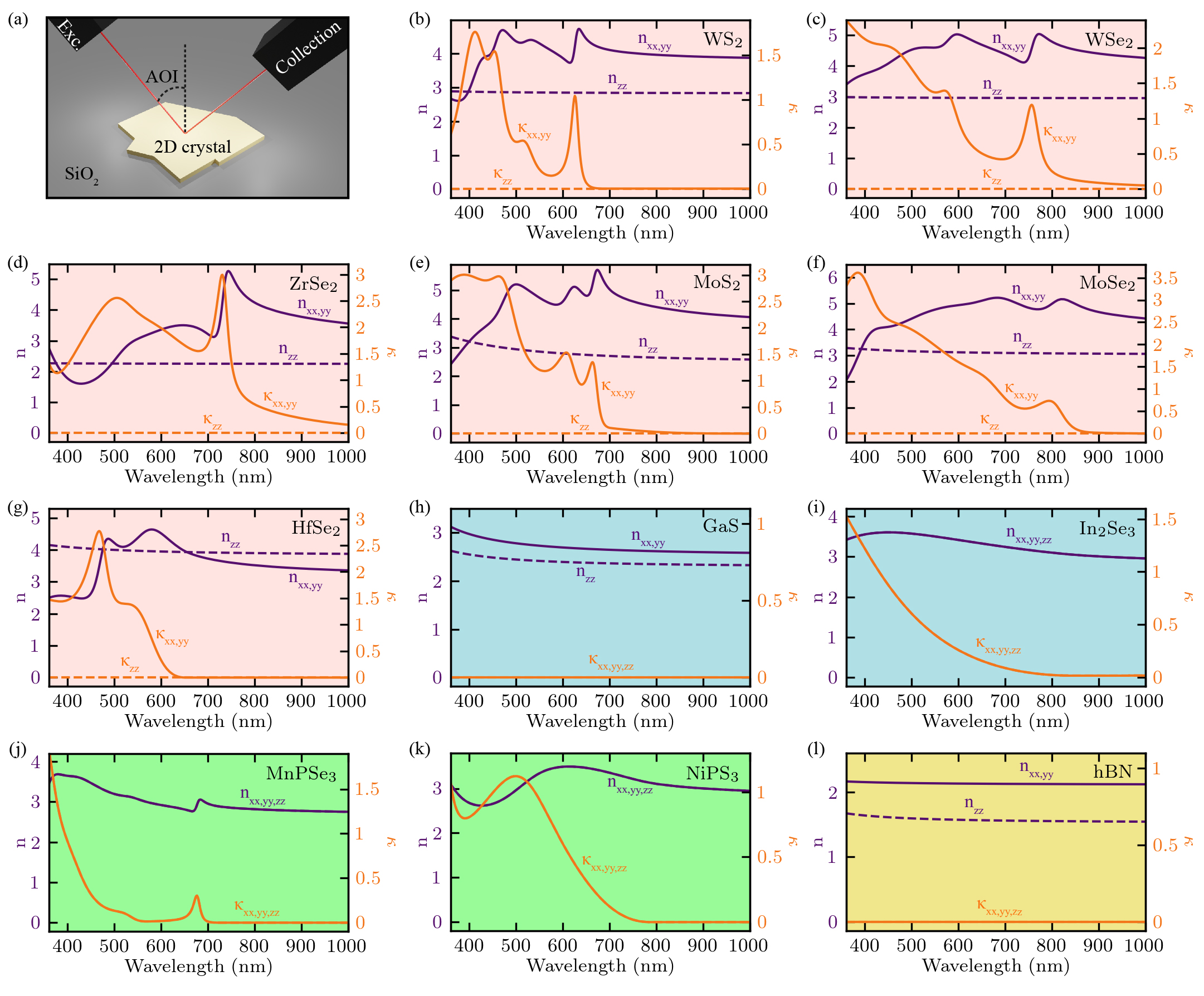
Linear optical properties of van der Waals materials As a first step in characterizing vdW crystals for nanophotonics fabrication, we extract the refractive index and extinction coefficient of a number popular materials including insulating hBN, TMDs, III-VI and magnetic materials. We begin by mechanically exfoliating multilayer crystals of 11 different vdW materials onto a 97 nm SiO2 on silicon substrate. We characterize the thickness of each crystal via AFM and measure the complex reflectance ratio of each sample via spectroscopic micro-ellipsometry, recording the amplitude () and phase () at three different angles of incidence (see supplementary Note 1), schematically shown in Figure 1(a). Each set of data is fitted with an appropriate multilayer model yielding the real () and imaginary () components of the complex refractive index shown in Figure 1(b)-(l) for each material including many members of the transition metal dichalcogenide family (WS2, WSe2, MoS2, MoSe2, ZrSe2, HfSe2), which are faintly shaded in red; two III-VI materials (GaS, In2Se3), which are shaded in blue; two magnetic layered materials (MnPSe3, NiPS3), which are shaded in green; and the insulating hBN, which is shaded in yellow.
We use an analytical model appropriate to each material based on two considerations: the presence or absence of an absorption bandgap within the experimentally achievable wavelength range (360 - 1000 nm) and any anisotropy in the dielectric response due to crystallographic asymmetry. Therefore, we divided the 11 materials into three categories (see supplementary Note 1) which are: semiconductors with a large bandgap (GaS, hBN), TMDs (WS2, WSe2, MoS2, MoSe2, ZrSe2, HfSe2) and isotropic materials (In2Se3, MnPSe3, NiPS3). We observe very strong absorption resonances, leading to high refractive indices, for well studied TMDs such as WS2, WSe2, MoS2 and MoSe2 which has been confirmed by previous reports in monolayers [41]. We also see prominent absorption resonances for ZrSe2, HfSe2, MnPSe3 and NiPS3 suggesting there may be a similar response in these materials. An interesting note here is that due to the strong binding energy of excitons in these materials, they are confined to individual layers and therefore, absorption processes can be ascribed to an in-plane regime while the out-of-plane regime remains transparent. This suggests that these materials are transparent for light propagating in-plane with an out-of-plane electric field. This anisotropy in the dielectric response results in especially high values of birefringence ( 3.0) observed for MoS2 and ZrSe2 near their lowest energy excitonic resonances in near-infrared wavelengths (see Supplementary Note 2).
The extracted refractive indices and extinction coefficients for GaS, hBN, MoS2, MoSe2, WS2, WSe2 and In2Se3 are in good agreement with previously reported values [42, 23, 43, 36, 22, 44], corroborating our approach. The extinction coefficients we extract for HfSe2, ZrSe2 and NiPS3, which to the best of our knowledge have not been previously reported, are consistent with DFT calculations of absorption in NiPS3 [45], HfSe2 and ZrSe2 [46], as well as experimentally measured absorption in NiPS3 [47].
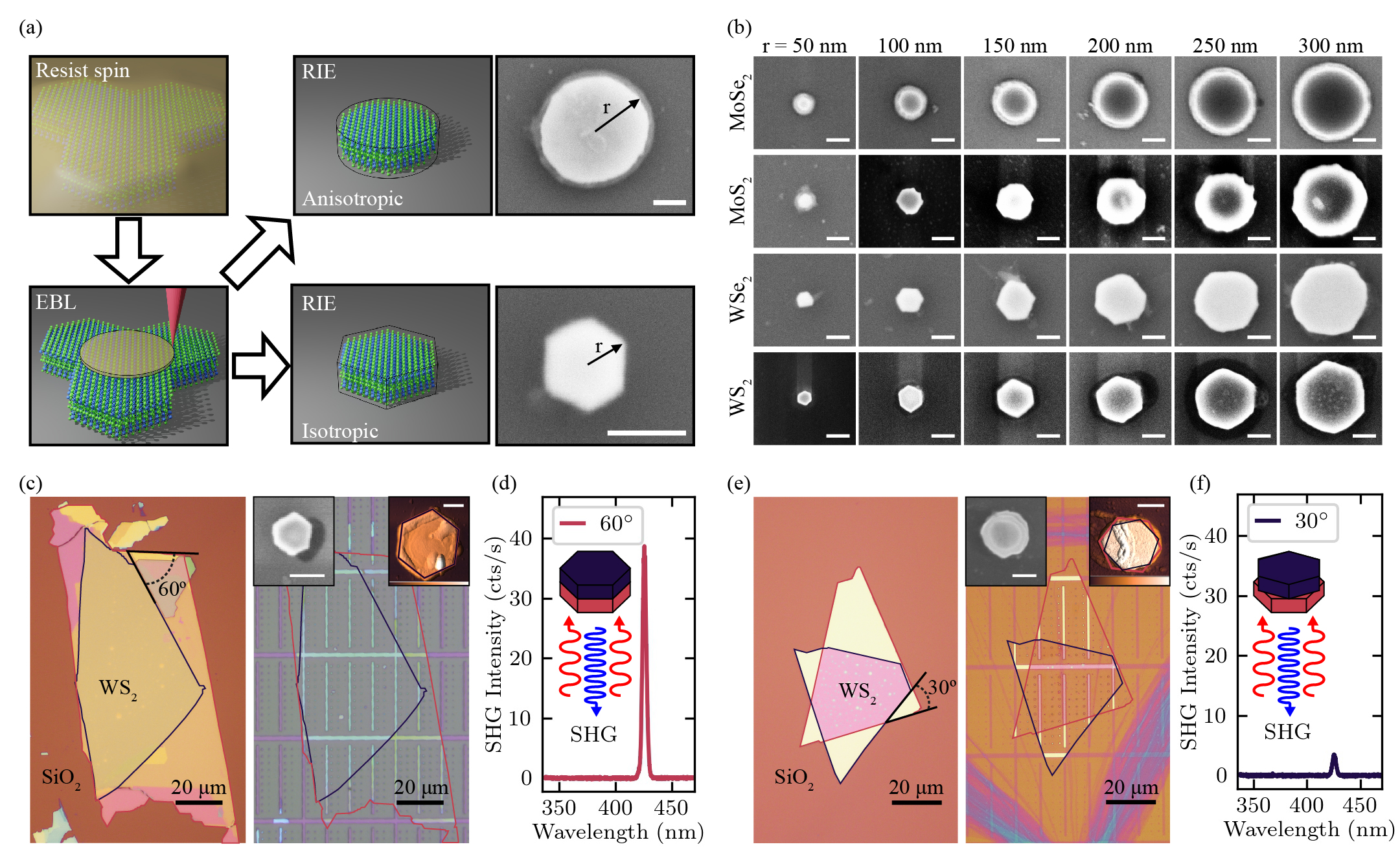
Nanoresonator fabrication In order to demonstrate the ease of fabrication of layered materials in the fabrication of nanophotonic structures, we pattern nanopillars into many of the optically studied materials. After mechanical exfoliation of multilayered crystals of each material onto a nominally 290 nm SiO2 on silicon substrate, we spun a positive resist onto the sample and patterned it into arrays of disks with varying radii using electron beam lithography (EBL). After development, the resist pattern was transferred into the layered crystals via reactive ion etching (RIE, see Methods) yielding monomer and dimer geometries. Figure 2(a) displays a schematic representation of the fabrication process which results in differing geometries in some TMDs, namely circular and hexagonal as a result of an anisotropic and isotropic etch respectively. This is due to etch selectivity in the armchair as opposed to the zigzag crystal axis [28, 48, 32, 49].
It may be expected that all TMDs will result in similar geometries after an isotropic fabrication procedure due to their identical crystal symmetry, however, this is not observed as shown in Figure 2(b). For a small nanopillar radius of r = 50 nm, WS2, WSe2 and MoS2 result in a hexagonal geometry, however, this is not true for MoSe2 which yields a circular geometry. For larger nanopillar radii, most of the materials also result in a circular geometry with the exception of WS2 which maintains a hexagonal shape up to a radius of 300 nm. The transition from hexagonal to circular geometry can be seen at a radius of 150 nm for MoS2 and 250 nm for WSe2. As these crystals have undergone the same etching conditions for the same amount of time, this suggests that ionized fluorine radicals react with and remove some materials faster than others, leading to a hexagonal geometry in larger structures of certain TMDs [49]. This is supported by theoretical calculations and experimental results for the enthalpy of formation of each material: -120.2 kJ/mol(WS2,[50]), -185.3 kJ/mol(WSe2,[51]), -234.2 kJ/mol(MoSe2,[52]), -271.8 kJ/mol(MoS2,[51]), where the increasingly negative values indicate a more stable material. Thus, the less negative values suggest that dissociation of materials such as WS2 and WSe2 requires less energy than MoS2 and MoSe2. An additional contribution to the formation of a hexagonal geometry is the crystal thickness of each of the etched materials, which are as follows: 43 nm(WS2), 85 nm(WSe2), 78 nm(MoS2), 29 nm(MoSe2). A smaller thickness leads to less surface area for etching in plane and thus results in less hexagonal nanopillars. These two contributions of the crystal thickness and the enthalpy of formation suggest relative etching speeds of TMD materials which can be ranked as: WS2 > WSe2 > MoS2 MoSe2.
Fabrication of hBN and HfSe2 nanopillars yields a circular geometry regardless of which previously employed etching recipes was used (see Supplementary Note 3) suggesting low or no crystal axis selectivity. Nanopillars in GaS also yield a circular geometry (Supplementary Note 3), although, the etching step was changed to employ a chlorine gas due to the poor reactivity of fluorine radicals with this material (see Methods). Similar to WS2, fabrication of ZrSe2 can yield both circular and hexagonal geometries up to a radius of 400 nm depending on the etching recipe used (Supplementary Note 3) suggesting a similarly fast etching speed and low enthalpy of formation. Subsequent attempts to etch In2Se3, NiPS3 and MnPSe3 with all etching recipes involving fluorine and chlorine gases yielded a very poor etch rate which did not form any appreciable nanostructures in the thin-film crystals (see Supplementary Note 3). Different methods of etching involving other gasses or wet etching may yield more satisfactory results, however, this is beyond the scope of this work.
In order to demonstrate the fabrication possibilities enabled by using vdW materials for nanophotonics, we also etched single nanopillars into twisted homostructures achieved by the stacking of two WS2 thin-film crystals via an all-dry transfer technique (see Methods) available only to layered dielectrics. We fabricated nanopillars into two homostructures each of which consisted of two thin-film crystals stacked at 60∘ and 30∘ twist angles on SiO2 substrates as shown in the left panels of Figure 2(c) and (e) respectively. The thickness of the constituent crystals used in the fabrication of the homostructures was 50 nm and 30 nm for the 60∘ and 30∘ twist angle samples respectively. Utilizing EBL pattering and isotropic etching, we obtained single nanopillars with heights of 100 nm and 60 nm for the 60∘ and 30∘ twisted homostructures as shown in the right panels of Figure 2(c) and (e) respectively. As the crystal axes of each constituent thin-film crystal in the homostructure are rotated with respect to each other due to the twist angle, the isotropic etching step will result in a rotated hexagonal structure for each. This rotation is not visible in the nanopillars of the 60∘ sample, shown in the insets of the right panel of Figure 2(c), as the twist angle will yield hexagonal structures which form directly above each other. However, the 30∘ twist angle is visible in the nanopillars fabricated from the other homostructure shown in the insets of the right panel of Figure 2(e) as this yields hexagonal structures with a 30∘ rotation. The twist angle in an unetched portion of the crystal was confirmed with SHG experiments, which yielded a brighter signal from the 60∘ homostructure when compared to the 30∘ sample (see Supplementary Note 4). This result is expected as the thickness of the WS22 homostructures was far below the coherence length of the SHG signal in this material and the centrosymmetry at the interface between the two constituent crystals was increasingly broken with twist angle [26]. This same bright SHG signal was also observed for 60∘ nanopillar structures as opposed to those fabricated in the 30∘ homostructures (r = 290 nm for both homostructures) as shown by the spectra plotted in Figures 2(d) and (f). This confirms that the broken centrosymmetry of the interface is consistent for both the unetched crystal and nanopillar structures as no additional enhancement observed from photonic resonances.
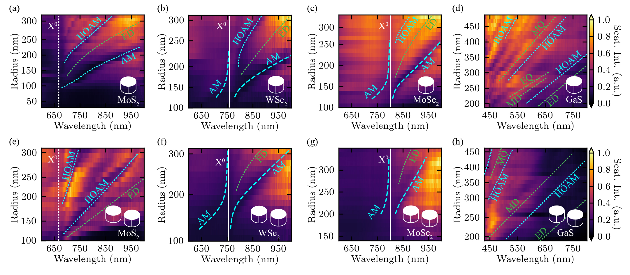
Photonic resonances of fabricated nanoantennas We subsequently studied the fabricated single and double nanopillar structures from a range of these materials using dark field spectroscopy. The height, radius and dimer separation gap were measured using AFM and SEM techniques. Figures 3(a)-(d) show the dark field spectra of monomer nanopillars over a range of radii for different layered materials including MoS2 (h = 70 nm), MoSe2 (h = 35 nm), WSe2 (h = 85 nm) and GaS (h = 200 nm). When compared with simulations of the scattering cross section expected for these nanostructures, we observed close agreement enabling us to identify neutral excitonic absorption in the material (X0), geometric Mie resonances such as magnetic dipole (MD), electric dipole (ED), magnetic quadrupole (MQ) and electric quadrupole (EQ) resonances as well as light-confining anapole (AM) and higher order anapole (HOAM) modes (see Supplementary Note 5). Similarly, we also measured the dark field spectra of dimers in MoS2 (h = 190 nm), MoSe2 (h = 30 nm), WSe2 (h = 45 nm) and GaS (h = 145 nm) with gaps ranging from 50 to 200 nm, shown in Figure 3(e)-(h) and compared these to simulations (see Supplementary Note 5) which also agreed well, demonstrating the possibility of realizing more complex nanophotonic architectures. Additionally we have measured the dark field spectra of monomers and dimers fabricated from WS2 and hBN which also yield similar resonances (see Supplementary Note 6). For GaS and hBN, we observe the formation of resonances at near-ultraviolet wavelengths due to the lack of absorption in these materials. We also observe a multitude of higher-order peaks in the dark field spectra of GaS monomer nanoantennas which are a result of a superposition of multiple Mie resonances, such as a magnetic and electric quadrupole as well as an electric dipole mode. Due to fabrication imperfections, some of the peaks are more or less prominent in the experimental than the simulated spectra. The WS2 twisted homostructure monomers shown in Figure 2(c) and (e) also yielded Mie and anapole resonances (see Supplementary Note 4) confirming them to be nanoantennas.
Focusing solely on the TMDs we observe an anticrossing of the anapole modes with the neutral exciton for TMD nanoantenna radii at which the energies of these two are expected to be degenerate providing evidence of strong light-matter coupling. As absorption is high at wavelengths below that of the X0, the higher order anapole resonance is not as clearly defined in this range and its signature minimum is not clearly visible in the data limiting our ability to fit this. We have, however, fitted the anticrossing of the anapole mode with the neutral exciton for WSe2 and MoSe2 monomers using a coupled oscillator model. We extracted an energy splitting of 141 meV for WSe2 monomers (r = 120 nm, h = 85 nm) as well as 100 meV for MoSe2 monomers (r = 135 nm, h = 35 nm). Using a previously reported condition which indicates that the coupling strength of the exciton and photon resonances must be larger than the average of the individual linewidths [53, 54] (see Supplementary Note 5), the measured energy splittings in WSe2 and MoSe2 monomers were confirmed to be evidence of strong light-matter coupling. A similar anticrossing was observed for dimer structures in WSe2 (132 meV for r = 155 nm, h = 45 nm), MoSe2 (104 meV for r = 215 nm, h = 30 nm) and WS2 (153 meV for r = 130 nm, h = 40 nm, see Supplementary Note 6). However, due to the larger linewidths of the neutral exciton and anapole resonances in these structures, the anticrossings do not satisfy the strong coupling condition instead indicating intermediate coupling by satisfying a complementary condition () [54]. FDTD simulations also confirm the strong and intermediate coupling between excitons and anapole modes yielding expected Rabi splitting as high as 200 meV for WSe2 monomers and 179 meV for WS2 dimers. Additionally, a higher order anapole mode is also observed to strongly couple to the exciton in simulations yielding Rabi splittings as high as 210 meV for WS2 monomers. Smaller experimental anticrossings were also observed for monomer nanoantennas fabricated from WS2 (see Supplementary Note 6) and MoS2, which was limited due fabrication imperfections in these nanostructures as well as large absorption at wavelengths below the neutral exciton resonance limiting our ability to accurately fit these features.
Dielectric nanoantennas on a metallic substrate We have demonstrated that the fabrication of vdW nanoresonators on a low refractive index substrate such as SiO2 is possible and results in well formed resonances in structures with heights as low as 30 nm. While this large index mismatch between substrate and nanoantenna may lead to tightly confined resonances, it can be advantageous to fabricate dielectric nanostructures onto a reflective substrate such as a gold mirror. This is expected to enable very high Q factor (103) dielectric-plasmonic modes which can provide very large Purcell factors (> 5000) [25]. We thus proceed to fabricate an array of WS2 monomer nanoantennas directly on a substrate with a 130 nm gold film. After exfoliation directly on the gold, similar to the technique used for a SiO2/Si substrate, EBL and RIE is used to define WS2 monomer nanoantennas with a circular and hexagonal geometry using the previously described recipes. An additional benefit to fabricating nanostructures in vdW materials onto a gold substrate arises due to the low etch rate of the gold compared to the previously used SiO2. This forms a natural etch stop which allows for a higher tolerance in fabrication errors concerning the etch rate and time.
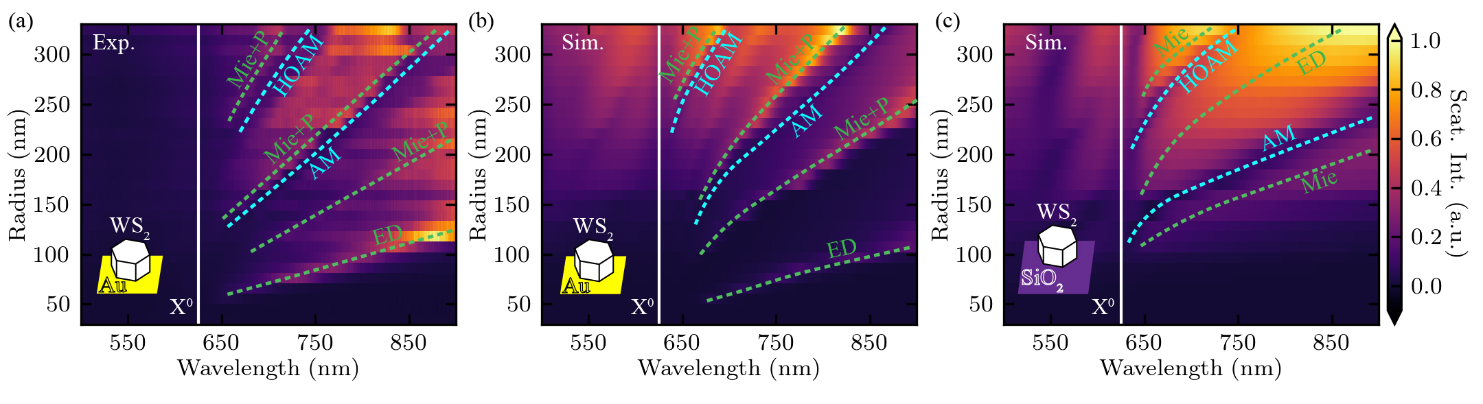
We subsequently record the dark field spectra of an array of the fabricated hexagonal WS2 monomer nanoantennas on gold, plotted in Figure 4(a). After characterization of the height (h = 62 nm) and radii of the nanoantennas using AFM and SEM respectively, we simulate the expected scattering intensity, shown in Figure 4(b) and observe close agreement with experiment. This allows us to identify Mie and anapole modes similar to those found in the nanostructures fabricated on SiO2.
In order to compare these structures to those previously fabricated on a low refractive index substrate, we also simulate the scattering intensities of identical WS2 hexagonal monomer nanoantennas onto a SiO2 substrate, displayed in Figure 4(c). Similar resonances are identified in these nanostructures, however, we observe a blueshifted ED mode and redshifted anapole modes which appear broader than those recorded for a gold substrate. For larger radii, we observe the appearance of additional modes in the nanoantennas fabricated on a gold substrate which we attribute to the formation of hybrid Mie-plasmonic (Mie+P) resonances. A plasmonic contribution may also be present for smaller nanoantenna radii, hybridizing with and enhancing spectral features which we identified as dielectric Mie (ED) and anapole resonances [25] due to mirror charge currents in the gold which respond to the induced bound charge currents in the WS2 nanoantennas. The reduced broadening of resonances in the nanostructures fabricated on gold leads us to consider the confinement of the electric field inside and in close proximity to the nanoantenna structure. Electric field intensity profiles recorded in and surrounding a WS2 monomer nanoantenna at the anapole and electric dipole modes for a gold and SiO2 substrate reveal differing confinements, shedding light on the origin of the mode shift, as well as increased intensities by at least an order of magnitude (see Supplementary Note 7). These suggest that the contribution of plasmonic resonances to the observed features in scattering may not be negligible.
Additionally, we compare the quality factors of the identified ED resonance in monomer nanoantennas fabricated from different vdW materials on a gold and SiO2 substrate both in simulation and experiment as shown by Table 1. The ED resonance was chosen as it was observed in all of the experimentally studied nanoantennas and leads to a high outcoupling of emitted light, which is important for most nanophotonic applications. The black and orange numbers correspond to a SiO2 and gold substrate respectively. Each value was extracted from a lorentzian fit of a resonance peak in scattering for a monomer nanoantenna geometry yielding a mode far from any anticrossings. For all materials, the extracted quality factors of resonances in nanostructures on a gold substrate yield higher values than for a SiO2 substrate in both experiment and simulation as suggested by the large reduction in broadening observed in Figure 4(a) and (b) when compared to Figure 4(c). Previously reported Mie resonances in dielectric monomer nanoantennas [55, 56] also yield lower quality factors than observed in our vdW nanoantennas on gold. These results suggest that the hybridization of Mie and plasmonic resonances may provide a large contribution to the quality factor improvement.
Some applications may require the placement of nanophotonic structures onto substrates which can be damaged by standard nanofabrication techniques such as biological samples [12] or substrates with deposited monolayer TMDs. We show that the nanoantennas we fabricate can be transferred onto such sensitive surfaces by taking advantage of their weak van der Waals adhesion to the substrate. Supplementary Note 8 shows the transfer of WS2 hexagonal nanoantennas onto a monolayer and bilayer WSe2 crystal which has been previously deposited onto a gold substrate. This regime of nanostructure fabrication, which we name "transferable photonics", enables the formation of tightly confined hotspots which can provide many orders of magnitude enhancement to emission sources, previously demonstrated for plasmonic structures [9], as well as applications which contain sensitive samples that may be damaged by standard nanofabrication techniques. Further development of this method is required in order to achieve a more controlled pick up and transfer of the nanostructures, which may prove easier for other nanoresonators such as photonic crystal cavities or metasurfaces [57], however, this is beyond the scope of this work.
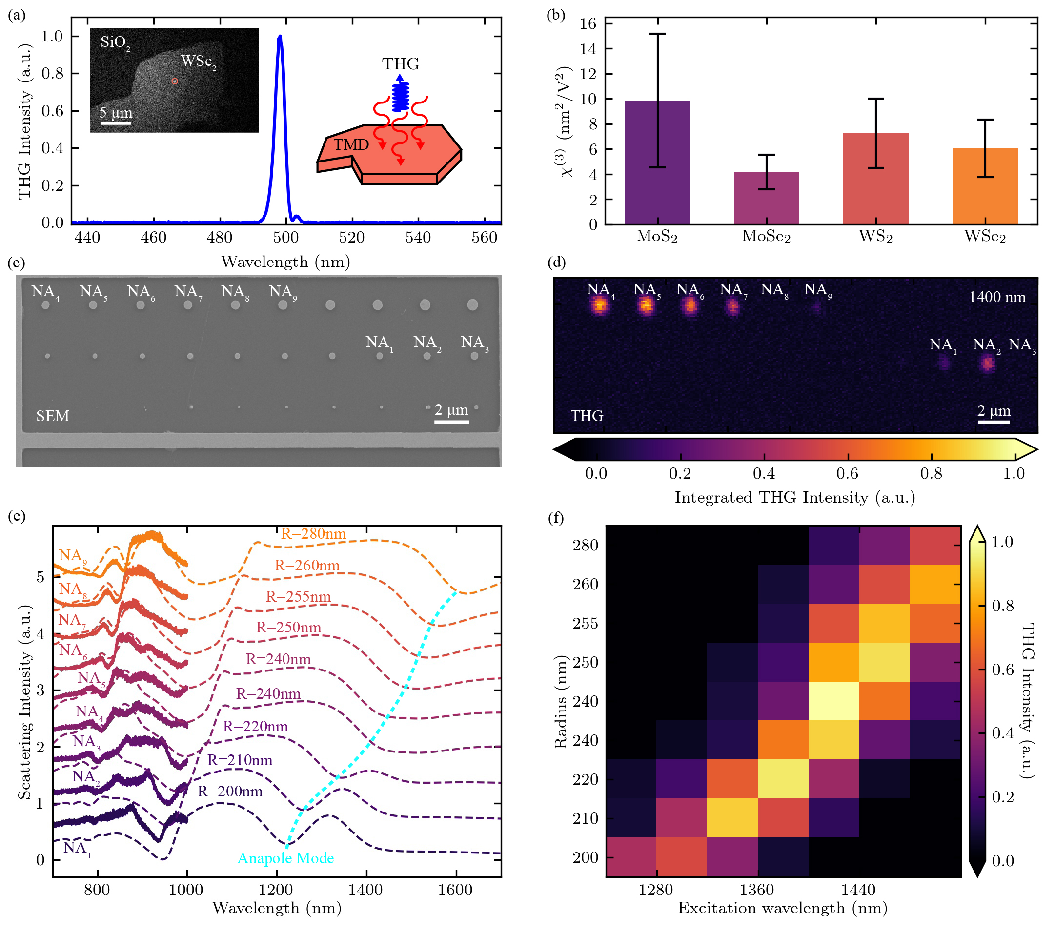
Nonlinear optical properties and applications As there is a large interest in employing vdW materials for enhancing nonlinear light applications [30, 37, 28, 38], we asses the viability of the most widely used TMDs for higher harmonic generation by exciting several thin-film crystals from each material with 220 fs laser pulses, nominally centered at 1500 nm. Figure 5(a) displays the third harmonic generation spectrum from a WSe2 thin-film crystal. The THG signal is observed at 498 nm (as the excitation has drifted to 1494 nm), with a small shoulder that we attribute to the laser spectrum, which also exhibits this feature. We observe a strong THG signal from this and other TMD materials and thus we extract the third harmonic susceptibility () for each by comparing our recorded THG intensity with nonlinear scattering theory [58] coupled with transfer-matrix method simulations (see Supplementary Note 9). The extracted values are plotted in Figure 5(b) where the error bars indicate the uncertainty in the measurement of the thickness of each thin-film crystal via AFM. The third harmonic susceptibilities we extract are up to an order of magnitude higher than for monolayers of the same material [59, 60], which is expected due to the difference in nonlinear properties between monolayer and multilayer crystals as well as the strong thickness dependence of the model used to to extract the values. These values are also up to 4 orders of magnitude larger than in BBO crystals regularly used for laser frequency tripling [61]. We observe the highest third harmonic susceptibility in MoS2 and the lowest in MoSe2.
Next, we pattern monomer nanoantennas with varying radii (r = 200 - 280 nm) into a WSe2 crystal with 250 nm thickness. An SEM image of the fabricated array is displayed in Figure 5(c). We record the dark field spectra of the nanoantennas in the visible range and compare these to simulations including both visible and near-infrared wavelengths which are in good agreement as shown in Figure 5(e). From the simulated infrared scattering intensity we observed an anapole mode scattering minimum redshifting from 1200 to 1600 nm with increasing nanoantenna radius, which can be used for enhancing higher harmonic generation. Thus, we illuminate the nanoantennas with a laser at a wavelength of 1400 nm and reposition our excitation and collection spot across the array of nanoantennas in order to record a map of the THG signal (see Methods). As shown in Figure 5(d), the THG signal is maximized at the position of certain nanoantennas (r = 240 nm) as opposed to others indicating a resonant coupling of the excitation laser leading to higher third harmonic signal. The nanoantennas which exhibit the brightest THG signal at 1400 nm illumination also exhibit an anapole mode minimum near this wavelength, as shown in Figure 5(e), providing further evidence for coupling of the excitation to the resonance of the nanoantenna. We subsequently vary the wavelength of the illumination source and observe the maximum THG signal shift from lower radius nanoantennas to those with a higher radius for an increasing excitation wavelength as shown in Figure 5(f) thereby confirming that the excitation is coupling to the anapole mode in the WSe2 monomer nanoantennas.
Discussion
We have studied a range of different vdW materials for their potential use as nanophotonic structures and demonstrated their advantages compared to traditional dielectric or plasmonic materials. We extract the dielectric response of 11 different layered materials via micro-ellipsometry. We observe very high refractive indices ( for some materials) when compared to Si or GaAs ( [62]) as well as a range of transparency windows from ultra-violet to near-infrared wavelengths. Utilizing material specific fitting models to extract the linear optical parameters leads to very high values of birefringence ( 3.0) in MoS2 and ZrSe2 as well as transparency for light propagating in-plane with an out-of-plane electric field in WS2, WSe2, MoS2, MoSe2, ZrSe2, HfSe2, GaS and hBN.
We fabricate nanoantenna structures in widely used vdW materials (MoS2, MoSe2, WS2, WSe2, hBN, HfSe2, ZrSe2, GaS). The geometries of nanostructures undergoing the same isotropic fabrication conditions provide insight into the etching speed of some TMDs which can be ranked as: ZrSe2 WS2 > WSe2 > MoSe2 MoS2. Etching of In2Se3, MnPSe3 and NiPS3 nanoantennas is beyond the scope of this work, however, our attempts with fluorine and chlorine gasses using both isotropic and anisotropic conditions indicate that other RIE or wet etching approaches will be necessary. Nanoantenna fabrication in MnPSe3 and NiPS3 may lead to optical control of the magnetic properties of these materials via coupling to a magnetic dipole mode. Additionally, our demonstration of monomer nanoantennas in twisted WS2 homostructures provides a straightforward route for future fabrication of heterostructure nanophotonic resonators such as 3D photonic crystal cavities or moire architectures [63] with integrated emissive materials, such as monolayer TMDs, enabled by the the weak van der Waals adhesion of layered dielectrics. The SHG signal observed from the interface of the twisted WS2 homostructure, with a thickness far below the coherence length in this material, can be enhanced due to coupling with the anapole mode in nanoantennas and may provide insights into interlayer excitons in multilayer TMD crystals.
Dark field spectroscopy of the fabricated structures in MoS2, MoSe2, WS2, WS2 twisted homostructures, WSe2, GaS and hBN on SiO2 yields well defined Mie and anapole resonances from ultra-violet to near-infrared wavelengths. Strong coupling within single nanostructures was observed at room temperature in several TMD crystals with extracted Rabi splittings as high as 153 meV for WS2, 141 meV for WSe2 and 104 meV for MoSe2 nanoantennas. This is a factor of 5 larger than reported for monolayer TMDs in high Q microcavities [64, 65] and 1 to 2 orders of magnitude higher than in InGaAs [66], AlGaAs [67, 68] and AlGaN [69] multiple quantum wells in similar microcavities.
Evidence of the possibility of fabricating vdW nanostructures on virtually any substrate without the need for lattice matching is provided by the patterning of nanoantennas onto a SiO2 as well as gold substrate. This provides the possibility for straightforward realization of large refractive index contrast interfaces as well as the integration of dielectric and plasmonic nanophotonic devices [25]. The fabricated WS2 nanoantennas on gold yield highly confined resonances with improved Q factors which may be beneficial for a number of applications including Purcell enhancement of emission, quantum efficiency enhancement [25], collection efficiency enhancement, strong light matter coupling, optical trapping, and surface enhanced Raman spectroscopy among others. Additional possibilities, demonstrated by our deposition of pre-fabricated WS2 nanoantennas onto a WSe2 monolayer on a gold substrate, include the transfer of etched nanostructures from one substrate onto another which contains sensitive samples such as monolayer TMDs or biological samples.
We also characterize the nonlinear optical properties of some of the most widely studied vdW crystals by extracting the THG susceptibility of various thin-film TMDs near the telecom C band, advantageous for quantum applications [70], yielding values up to an order of magnitude higher than in monolayers [59, 60] and up to 4 orders of magnitude larger than in BBO crystals regularly used for laser frequency tripling applications [61]. We also explore a method of enhancing such nonlinear signals via coupling to resonances in monomer nanoantennas of WSe2.
Due to their high refractive indices, wide range of bandgaps and adhesive properties, vdW material nanostructures enable a wide variety of applications as shown by our demonstrations of twisted homostructure nanostructures, single nanoantenna strong coupling, hybrid high-Q Mie-Plasmonic modes, post-fabrication nanostructure deposition and THG enhancement. The advantages of using van der Waals materials will enable many exciting opportunities in nanophotonics.
Methods
Ellipsometry Spectroscopic ellipsometry measurements were carried out in the wavelength range 360 nm to 1000 nm with a spatial resolution of 1 m2 using a nulling imaging ellipsometer (EP4, Accurion Gmbh) in an inert Ar atmosphere at room temperature. Ellipsometric data from the samples were acquired at three different angles of incidence (AOI, defining the vertical as AOI = 0∘) at 45∘, 50∘ and 55∘.
Sample fabrication Van der Waals materials exfoliation: Layered material crystals were mechanically exfoliated from bulk (HQ-graphene) onto a nominally 290 nm SiO2 on silicon or gold substrate. Large crystals with recognizable axes via straight edged sides at 120∘ to each other were identified and their positions within the sample were recorded for further patterning.
Homostructure fabrication: The 60∘ and 30∘ stacked homostructures were fabricated with an all dry transfer technique. For the 60∘ homostructure, two separate 50 nm WS2 crystals were exfoliated onto a PPC/SiO2 substrate. These were then picked up consecutively with a 60∘ twist angle using a PMMA/PDMS membrane and deposited onto a SiO2 substrate. For the 30∘ homostructure, a single 30 nm WS2 crystal was exfoliated onto a PPC/SiO2 substrate and subsequently broken with the use of an AFM cantilever tip. Consecutive pick up of the two crystals with a 30∘ twist angle using a PMMA/PDMS membrane was followed by deposition onto another SiO2 substrate. Thicknesses were measured with AFM.
Electron beam lithography: Samples were spin coated with ARP-9 resist (AllResist GmbH) at 3500 rpm for 60 s and baked at 180∘ for 5 min yielding a film of 200 nm thickness. Electron beam lithography was performed in a Raith GmbH Voyager system operating at 50 kV using a beam current of 560 pA.
Reactive ion etching of TMDs and hBN: Anisotropic etching to imprint the resist pattern into the WS2 crystals physically was carried out using a mixture of CHF3 (14.5 sccm) and SF6 (12.5 sccm) at a DC bias of 180 V and a pressure of 0.039 mbar for 40 seconds. Isotropic etching was achieved by using a more chemical recipe with solely SF6 (30 sccm) at a DC bias of 40 V and a pressure of 0.13 mbar for 40 seconds. Removal of the remaining resist after etching was accomplished by a bath in warm 1165 resist remover (1 hour) followed by Acetone (5 min) and IPA (5 min). If resist is still found on the sample, final cleaning is done in a bath of Acetone (1 hour) and IPA (5 min) followed by 1 hour in a UV ozone treatment. In some cases, the structures were slightly over-etched leading to nanoantennas with a small pedestal of SiO2 (<20 nm) or gold (<5 nm). This, however, did not lead to any noticeable changes in the photonic resonances.
Reactive ion etching of GaS: Isotropic etching of GaS was achieved with SiCl4 gas (5 sccm) at a pressure of 50 mTorr and DC bias of 175 V for 7 minutes. The resist removal step was the same as for other materials, however, this did not achieve proper removal of all resist from the sample. The residual resist did not noticeably impact the photonic resonances measured in dark field spectroscopy.
Gold substrate preparation: In order to prepare the gold substrate, we firstly deposit a 10 nm layer of Ti onto a 290nm SiO2/Si substrate via e-beam evaporation in order to improve the adhesion between substrate and gold. We subsequently deposit 130 nm of gold via the same method.
Dark field spectroscopy Optical spectroscopy in a dark field configuration was achieved using a Nikon LV150N microscope with a fiber-coupled output. Incident illumination from a tungsten halogen lamp in the microscope was guided to a circular beam block with a diameter smaller than the beam diameter. The light was then reflected by a 45∘ tilted annular mirror towards a 50x Nikon (0.8 NA) dark-field objective which only illuminates the sample at large angles to the normal. Reflected light from the sample is guided back through the same objective towards a fiber coupler. Due to the small diameter of the multimode fiber core used, only light reflected back at small angles to the normal is collected. The fiber from the microscope was subsequently coupled to a Princeton Instruments spectrometer and charge coupled device.
FDTD scattering simulations Calculations of the scattering cross section shown in Figure 4(c), 5(e) and Supplementary Notes 5 and 6 were carried out by defining the geometry of the vdW material nanoantennas onto a SiO2 or gold substrate utilizing the refractive indices extracted from the ellipsometry measurements. Illumination with a plane wave was sent normal to the surface using a TFSF source from the air side. The illumination was polarized parallel to the surface. The scattered intensity was subsequently collected from a monitor set above the illumination plane (in the far field) so that the dark field spectroscopy experiments could be closely emulated. The finite-difference time-domain simulations were carried out using Lumerical Inc. software.
Second Harmonic Generation In order to probe the second harmonic generated signal from the twisted homostructures and their nanopillars, as shown in Figure 2(d),(f) and Supplementary Note 4, we used a Mai-Tai Ti-sapphire mode-locked femtosecond laser as the excitation source set at 850 nm with an average power of 10 mW. The collimated laser light passed through a linear film polarizer, half wave plate, dichroic mirror and was incident on a 100x (0.7 NA) Mitutoyo objective which focused the excitation light onto the sample allowing us to probe single nanopillars and thin-film crystals. Second harmonic generated light was then collected using the same objective subsequently reflecting the light from the dichroic mirror and passing it through an analyzer. The collected light is then filtered by long-pass filters (650 nm cutoff) and fiber coupled to a multi-mode fiber and sent to a Princeton Instruments spectrometer and CCD to yield the data displayed in Figure 2(d) and (f) as well as in Supplementary Note 4.
Third Harmonic Generation THG measurements, shown in Figure 5, were carried out by illuminating the sample with 220 fs laser pulses (Yb:KGW Pharos, Light conversion) at 100 kHz repetition rate and a wavelength of 1500 nm through a 0.85 NA objective (60X). The laser beam was directed towards the sample via a dichroic mirror which transmits the visible THG signal at 500 nm and reflects the illuminating wavelength. The illuminating beam is subsequently focused onto the back focal plane of the objective using a 1X telescope (100 mm) and the power is attenuated through a rotational neutral density wheel. The excitation power is measured with an infrared power meter (Thorlabs, S122C). The collected THG signal intensity from the sample is measured via a Thorlabs camera (CS165MUM) calibrated to convert counts/pixel to an intensity. The beam size of the THG signal and the excitation beam is measured by fitting the camera counts from a reference gallium phosphide sample emitting a strong second harmonic signal with a Gaussian function. The final peak intensity of the excitation and third harmonic signal is calculated by adjusting the power measurements with the respective beam sizes.
Nanoantenna THG resonances were recorded using a piezoelectric stage to scan the sample over the region of interest while the generated signal was recorded with a single-photon detector (Picoquant, Micro Photon Devices). The excitation wavelength ranged from 1240 nm to 1480 nm with increments of 40 nm using an excitation power of 6.5 W. The reported THG intensity from each nanoantenna was determined using the counts of the single-photon detector and corrected with the beam size measurement so that excitation intensity fluctuations in this spectral range were taken into account.
Acknowledgments
P. G. Z., T.S.M., S.R., X.H., and A. I. T. acknowledge support from the European Graphene Flagship Project under grant agreement number 881603 and EPSRC grants EP/S030751/1, EP/V006975/1, and EP/V026496/1. L.S. acknowledges funding support through a Humboldt Research Fellowship from the Alexander von Humboldt Foundation. Y.W. acknowledges a Research Fellowship (TOAST) awarded by the Royal Academy of Engineering. We would also like to thank Prof. Keith McKenna for his contribution concerning the enthalpy of formation factor in the etching speed of different vdW materials.
Author Contributions
P.G.Z and T.S.M. exfoliated WS2, WSe2, MoSe2, MoS2, HfSe2, ZrSe2 hBN, GaS, In2Se3, MnPSe3 and NiPS3 crystals onto SiO2 substrates for ellipsometry measurements, nanoresonator fabrication and THG susceptibility measurements. D.A.P. and M.B.G performed ellipsometry measurements and fit the complex reflectance ratio with appropriate analytical models in order to extract the real and imaginary parts of the complex refractive index of each material. Y.W., X.H. and P.G.Z. fabricated nanoantenna structures using EBL and RIE. P.G.Z. performed SHG experiments to confirm the twist angle of the homostructures and their nanoantennas. P.G.Z., T.S.M. and S.R. performed all AFM characterization of crystal thickness and nanoantenna heights. P.G.Z., T.S.M. and S.R. performed all SEM measurements to characterize nanoantenna radii. P.G.Z., T.S.M. and S.R. recorded all all dark field spectra and analyzed the results. C.L. and P.G.Z. fit the experimental and simulated scattering data to a coupled oscillator model to provide evidence of strong coupling and extract Rabi splittings. P.G.Z. and T.S.M. performed all FDTD simulations of the scattering cross sections. P.G.Z. and X.H. transferred WS2 nanoantennas onto a monolayer WSe2 crystal on a gold substrate. T.H. and S.V. performed THG experiments on WSe2 nanoantennas as well as TMD thin-film crystals and subsequently analyzed the recorded spectra in order to extract values. T.F.K., B.D.G., R.S. and A.I.T. managed various aspects of the project. P.G.Z. and A.I.T. wrote the manuscript with contributions from all co-authors. P.G.Z., L.S., Y.W. and A.I.T. conceived the experiments and simulations. A.I.T. oversaw the entire project.
References
- [1] C. Jamois, R. B. Wehrspohn, L. C. Andreani, C. Hermann, O. Hess, and U. Gösele. Silicon-based two-dimensional photonic crystal waveguides. Photonics and Nanostructures - Fundamentals and Applications, 1(1):1–13, 2003.
- [2] B. Rigal, B. Dwir, A. Rudra, I. Kulkova, A. Lyasota, and E. Kapon. Single photon extraction and propagation in photonic crystal waveguides incorporating site-controlled quantum dots. Applied Physics Letters, 112(5):051105, 2018.
- [3] Peter Lodahl, Sahand Mahmoodian, and Soren Stobbe. Interfacing single photons and single quantum dots with photonic nanostructures. Reviews of Modern Physics, 87(2):347–400, 2015.
- [4] Javier Cambiasso, Gustavo Grinblat, Yi Li, Aliaksandra Rakovich, Emiliano Cortés, and Stefan A. Maier. Bridging the Gap between Dielectric Nanophotonics and the Visible Regime with Effectively Lossless Gallium Phosphide Antennas. Nano Letters, 17(2):1219–1225, 2017.
- [5] Feng Liu, Alistair J. Brash, John O’Hara, Luis M.P.P. Martins, Catherine L. Phillips, Rikki J. Coles, Benjamin Royall, Edmund Clarke, Christopher Bentham, Nikola Prtljaga, Igor E. Itskevich, Luke R. Wilson, Maurice S. Skolnick, and A. Mark Fox. High Purcell factor generation of indistinguishable on-chip single photons. Nature Nanotechnology, 13:835–840, 2018.
- [6] L. Sortino, P. G. Zotev, S. Mignuzzi, J. Cambiasso, D. Schmidt, A. Genco, M. Aßmann, M. Bayer, S. A. Maier, R. Sapienza, and A. I. Tartakovskii. Enhanced light-matter interaction in an atomically thin semiconductor coupled with dielectric nano-antennas. Nature Communications, 10:5119, 2019.
- [7] Sanfeng Wu, Sonia Buckley, John R. Schaibley, Liefeng Feng, Jiaqiang Yan, David G. Mandrus, Fariba Hatami, Wang Yao, Jelena Vučković, Arka Majumdar, and Xiaodong Xu. Monolayer semiconductor nanocavity lasers with ultralow thresholds. Nature, 520:69–72, 2015.
- [8] Gustavo Grinblat, Yi Li, Michael P. Nielsen, Rupert F. Oulton, and Stefan A. Maier. Efficient Third Harmonic Generation and Nonlinear Subwavelength Imaging at a Higher-Order Anapole Mode in a Single Germanium Nanodisk. ACS Nano, 11(1):953–960, 2017.
- [9] Rohit Chikkaraddy, Bart De Nijs, Felix Benz, Steven J. Barrow, Oren A. Scherman, Edina Rosta, Angela Demetriadou, Peter Fox, Ortwin Hess, and Jeremy J. Baumberg. Single-molecule strong coupling at room temperature in plasmonic nanocavities. Nature, 535:127–130, 2016.
- [10] Denis G. Baranov, Martin Wersäll, Jorge Cuadra, Tomasz J. Antosiewicz, and Timur Shegai. Novel Nanostructures and Materials for Strong Light-Matter Interactions. ACS Photonics, 5(1):24–42, 2018.
- [11] Kai Wang, Ethan Schonbrun, Paul Steinvurzel, and Kenneth B. Crozier. Trapping and rotating nanoparticles using a plasmonic nano-tweezer with an integrated heat sink. Nature Communications, 2:469, 2011.
- [12] Zhe Xu, Wuzhou Song, and Kenneth B. Crozier. Optical Trapping of Nanoparticles Using All-Silicon Nanoantennas. ACS Photonics, 5(12):4993–5001, 2018.
- [13] Donato Conteduca, Giuseppe Brunetti, Giampaolo Pitruzzello, Francesco Tragni, Kishan Dholakia, Thomas F. Krauss, and Caterina Ciminelli. Exploring the Limit of Multiplexed Near-Field Optical Trapping. ACS Photonics, 8(7):2060–2066, 2021.
- [14] Gleb M. Akselrod, Christos Argyropoulos, Thang B. Hoang, Cristian Ciracì, Chao Fang, Jiani Huang, David R. Smith, and Maiken H. Mikkelsen. Probing the mechanisms of large Purcell enhancement in plasmonic nanoantennas. Nature Photonics, 8(11):835–840, 2014.
- [15] Mäx Blauth, Marius Jürgensen, Gwenaëlle Vest, Oliver Hartwig, Maximilian Prechtl, John Cerne, Jonathan J. Finley, and Michael Kaniber. Coupling single photons from discrete quantum emitters in WSe2 to lithographically defined plasmonic slot-waveguides. Nano Letters, 18(11):6812–6819, 2018.
- [16] Yue Luo, Gabriella D. Shepard, Jenny V. Ardelean, Daniel A. Rhodes, Bumho Kim, Katayun Barmak, James C. Hone, and Stefan Strauf. Deterministic coupling of site-controlled quantum emitters in monolayer WSe2 to plasmonic nanocavities. Nature Nanotechnology, 13:1137–1142, 2018.
- [17] Jacob B. Khurgin. How to deal with the loss in plasmonics and metamaterials. Nature Nanotechnology, 10(1):2–6, 2015.
- [18] Reuben M. Bakker, Dmitry Permyakov, Ye Feng Yu, Dmitry Markovich, Ramón Paniagua-Domínguez, Leonard Gonzaga, Anton Samusev, Yuri Kivshar, Boris Lukyanchuk, and Arseniy I. Kuznetsov. Magnetic and electric hotspots with silicon nanodimers. Nano Letters, 15(3):2137–2142, 2015.
- [19] Denis G. Baranov, Dmitry A. Zuev, Sergey I. Lepeshov, Oleg V. Kotov, Alexander E. Krasnok, Andrey B. Evlyukhin, and Boris N. Chichkov. All-dielectric nanophotonics: the quest for better materials and fabrication techniques. Optica, 4(7):814, 2017.
- [20] Ruggero Verre, Denis G. Baranov, Battulga Munkhbat, Jorge Cuadra, Mikael Käll, and Timur Shegai. Transition metal dichalcogenide nanodisks as high-index dielectric Mie nanoresonators. Nature Nanotechnology, 14:679–683, 2019.
- [21] T. S. Moss. Relations between the Refractive Index and Energy Gap of Semiconductors. Physica Status Solidi (B), 131(2):415–427, 1985.
- [22] Battulga Munkhbat, Piotr Wróbel, Tomasz J. Antosiewicz, and Timur O. Shegai. Optical constants of several multilayer transition metal dichalcogenides measured by spectroscopic ellipsometry in the 300-1700 nm range: high-index, anisotropy, and hyperbolicity. ACS Photonics, 2022.
- [23] Yoonhyuk Rah, Yeonghoon Jin, Sejeong Kim, and Kyoungsik Yu. Optical analysis of the refractive index and birefringence of hexagonal boron nitride from the visible to near-infrared. Optics Letters, 44:3797–3800, 2019.
- [24] Yuan Liu, Yu Huang, and Xiangfeng Duan. Van der Waals integration before and beyond two-dimensional materials. Nature, 567(7748):323–333, 2019.
- [25] Yi Yang, Owen D. Miller, Thomas Christensen, John D. Joannopoulos, and Marin Soljačić. Low-Loss Plasmonic Dielectric Nanoresonators. Nano Letters, 17(5):3238–3245, 2017.
- [26] Kaiyuan Yao, Nathan R. Finney, Jin Zhang, Samuel L. Moore, Lede Xian, Nicolas Tancogne-Dejean, Fang Liu, Jenny Ardelean, Xinyi Xu, Dorri Halbertal, K. Watanabe, T. Taniguchi, Hector Ochoa, Ana Asenjo-Garcia, Xiaoyang Zhu, D. N. Basov, Angel Rubio, Cory R. Dean, James Hone, and P. James Schuck. Enhanced tunable second harmonic generation from twistable interfaces and vertical superlattices in boron nitride homostructures. Science Advances, 7(10):1–8, 2021.
- [27] A. K. Geim and I. V. Grigorieva. Van der Waals heterostructures. Nature, 499(7459):419–425, 2013.
- [28] Panaiot G Zotev, Yue Wang, Luca Sortino, Toby Severs Millard, Nic Mullin, Donato Conteduca, Mostafa Shagar, Armando Genco, Jamie K Hobbs, Thomas F Krauss, and Alexander I Tartakovskii. Transition Metal Dichalcogenide Dimer Nanoantennas for Tailored Light-Matter Interactions. ACS Nano, 16(4):6493–6505, 2022.
- [29] Joshua D Caldwell. Photonics with hexagonal boron nitride. Nature Reviews Materials, 4(August), 2019.
- [30] Sebastian Busschaert, Moritz Cavigelli, Ronja Khelifa, Achint Jain, and Lukas Novotny. TMDC Resonators for Second Harmonic Signal Enhancement. ACS Photonics, 7(9):2482–2488, 2020.
- [31] Xingwang Zhang, Xiaojie Zhang, Wenzhuo Huang, Kedi Wu, Mengqiang Zhao, A. T. Charlie Johnson, Sefaattin Tongay, and Ertugrul Cubukcu. Ultrathin WS2-on-Glass Photonic Crystal for Self-Resonant Exciton-Polaritonics. Advanced Optical Materials, 8:1901988, 2020.
- [32] Battulga Munkhbat, Betül Küçüköz, Denis G. Baranov, Tomasz J. Antosiewicz, and Timur O. Shegai. Nanostructured transition metal dichalcogenide multilayers for advanced nanophotonics. arXiv, pages 1–21, 2022.
- [33] Meibao Qin, Junyi Duan, Shuyuan Xiao, Wenxing Liu, Tianbao Yu, Tongbiao Wang, and Qinghua Liao. Strong coupling between excitons and quasi-Bound states in the continuum in the bulk transition metal dichalcogenides. arXiv, 2022.
- [34] Thomas Weber, Luca Sortino, Amine Ben Mhenni, Nathan P Wilson, Jonathan J Finley, Stefan A Maier, and Andreas Tittl. Strong light-matter interaction with self-hybridized bound states in the continuum in monolithic van der Waals metasurfaces. arXiv, 2022.
- [35] Huiqin Zhang, Bhaskar Abhiraman, Qing Zhang, Jinshui Miao, Kiyoung Jo, Stefano Roccasecca, Mark W. Knight, Artur R. Davoyan, and Deep Jariwala. Hybrid exciton-plasmon-polaritons in van der Waals semiconductor gratings. Nature Communications, 11:3552, 2020.
- [36] G. A. Ermolaev, D. V. Grudinin, Y. V. Stebunov, V. G. Kravets, J. Duan, G. I. Tselikov, K. V. Voronin, D. I. Yakubovsky, S. M. Novikov, D. G. Baranov, A. Y. Nikitin, T. Shegai, P. Alonso-González, A. N. Grigorenko, A. V. Arsenin, K. S. Novoselov, and V. S. Volkov. Giant optical anisotropy in transition metal dichalcogenides for next-generation photonics. Nature Communications, 12:854, 2021.
- [37] Anna Popkova, Ilya Antropov, Gleb I. Tselikov, Georgy A. Ermolaev, Igor Ozerov, Roman V. Kirtaev, Sergey M. Novikov, Evlyukhin Andrey B., Aleksey V. Arsening, Vladimir O. Bessonov, Valentyn S. Volkov, and Andrey A. Fedyanin. Nonlinear Exciton-Mie Coupling in Transition Metal Dichalcogenide Nanoresonators. Laser and Photonics Reviews, page 2100604, 2022.
- [38] Xinyi Xu, Chiara Trovatello, Fabian Mooshammer, Yinming Shao, Shuai Zhang, Kaiyuan Yao, D. N. Basov, Giulio Cerullo, and P. James Schuck. Towards compact phase-matched and waveguided nonlinear optics in atomically layered semiconductors. Nature Photonics, 2022.
- [39] Naseer Muhammad, Yang Chen, Cheng Wei Qiu, and Guo Ping Wang. Optical Bound States in Continuum in MoS2-Based Metasurface for Directional Light Emission. Nano Letters, 21(2):967–972, 2021.
- [40] Haonan Ling, Renjie Li, and Artur R. Davoyan. All van der Waals Integrated Nanophotonics with Bulk Transition Metal Dichalcogenides. ACS Photonics, 8(3):721–730, 2021.
- [41] Yilei Li, Alexey Chernikov, Xian Zhang, Albert Rigosi, Heather M Hill, Arend M Van Der Zande, Daniel A Chenet, En-min Shih, James Hone, and Tony F Heinz. Measurement of the optical dielectric function of monolayer transition-metal dichalcogenides: MoS2, MoSe2, WS2, and WSe2. Physical Review B, 90:205422, 2014.
- [42] Kiyoshi Kato and Nobuhiro Umemura. Sellmeier equations for GaS and GaSe and their applications to the nonlinear optics in GaSxSe1-x. Optics Letters, 36(5):746, 2011.
- [43] A. Segura, L. Artús, R. Cuscó, T. Taniguchi, G. Cassabois, and B. Gil. Natural optical anisotropy of h-BN: Highest giant birefringence in a bulk crystal through the mid-infrared to ultraviolet range. Physical Review Materials, 2(2):1–6, 2018.
- [44] Yujin Cho, Sean M. Anderson, Bernardo S. Mendoza, Shun Okano, Ramon Carriles, N. Arzate, Anatoli I. Shkrebtii, Di Wu, Keji Lai, D. R. T. Zahn, and M. C. Downer. Opto-electronic properties of alpha-In2Se3: single-layer to bulk. arXiv, pages 1–9, 2019.
- [45] So Yeun Kim, Tae Yun Kim, Luke J. Sandilands, Soobin Sinn, Min Cheol Lee, Jaeseok Son, Sungmin Lee, Ki Young Choi, Wondong Kim, Byeong Gyu Park, C. Jeon, Hyeong Do Kim, Cheol Hwan Park, Je Geun Park, S. J. Moon, and T. W. Noh. Charge-Spin Correlation in van der Waals Antiferromagnet NiPS3. Physical Review Letters, 120(13):136402, 2018.
- [46] Hemendra Nath Jaiswal, Maomao Liu, Simran Shahi, Fei Yao, Qiyi Zhao, Xinlong Xu, and Huamin Li. Localized surface plasmon resonance. arXiv, pages 1–24, 2018.
- [47] Christopher Lane and Jian Xin Zhu. Thickness dependence of electronic structure and optical properties of a correlated van der Waals antiferromagnetic NiPS3 thin film. Physical Review B, 102(7):1–8, 2020.
- [48] Battulga Munkhbat, Andrew B Yankovich, Denis G. Baranov, Ruggero Verre, Eva Olsson, and Shegai Timur. Transition metal dichalcogenide metamaterials with atomic precision. Nature Communications, 11:4604, 2020.
- [49] Dorte R. Danielsen, Anton Lyksborg-Andersen, Kirstine E.S. Nielsen, Bjarke S. Jessen, Timothy J. Booth, Manh Ha Doan, Yingqiu Zhou, Peter Bøggild, and Lene Gammelgaard. Super-Resolution Nanolithography of Two-Dimensional Materials by Anisotropic Etching. ACS Applied Materials and Interfaces, 13(35):41886–41894, 2021.
- [50] Shuang Chen, Yong Pan, Dajun Wang, and Hong Deng. Structural Stability and Electronic and Optical Properties of Bulk WS2 from First-Principles Investigations. Journal of Electronic Materials, 49(12):7363–7369, 2020.
- [51] P. A.G. O’Hare, Brett M. Lewis, and B. A. Parkinson. Standard molar enthalpy of formation by fluorine-combustion calorimetry of tungsten diselenide (WSe2). Thermodynamics of the high-temperature vaporization of WSe2. Revised value of the standard molar enthalpy of formation of molybdenite (MoS2). The Journal of Chemical Thermodynamics, 20(6):681–691, 1988.
- [52] P. A.G. O’Hare, I. R. Tasker, and J. M. Tarascon. A fluorine-combustion calorimetric study of two molybdenum selenides: MoSe2 and Mo6Se6. The Journal of Chemical Thermodynamics, 19(1):61–68, 1987.
- [53] D. S. Dovzhenko, S. V. Ryabchuk, Yu P. Rakovich, and I. R. Nabiev. Light-matter interaction in the strong coupling regime: Configurations, conditions, and applications. Nanoscale, 10(8):3589–3605, 2018.
- [54] Shiyu Shen, Yuyang Wu, Yuhang Li, Peng Xie, Qi Ding, Xiaoyu Kuang, Wenxin Wang, and Wei Wang. Tuning magnetic Mie-exciton interaction from the intermediate to strong coupling regime in a WSe 2 monolayer coupled with dielectric-metal nanoresonators . Physical Review B, 105(15):1–9, 2022.
- [55] Andrey E. Miroshnichenko, Andrey B. Evlyukhin, Ye Feng Yu, Reuben M. Bakker, Arkadi Chipouline, Arseniy I. Kuznetsov, Boris Luk’yanchuk, Boris N. Chichkov, and Yuri S. Kivshar. Nonradiating anapole modes in dielectric nanoparticles. Nature Communications, 6:8069, 2015.
- [56] Maria Timofeeva, Lukas Lang, Flavia Timpu, Claude Renaut, Alexei Bouravleuv, Igor Shtrom, George Cirlin, and Rachel Grange. Anapoles in Free-Standing III-V Nanodisks Enhancing Second-Harmonic Generation. Nano Letters, 18(6):3695–3702, 2018.
- [57] Chang Hua Liu, Jiajiu Zheng, Shane Colburn, Taylor K. Fryett, Yueyang Chen, Xiaodong Xu, and Arka Majumdar. Ultrathin van der Waals Metalenses. Nano Letters, 18(11):6961–6966, 2018.
- [58] Kevin O’Brien, Haim Suchowski, Junsuk Rho, Alessandro Salandrino, Boubacar Kante, Xiaobo Yin, and Xiang Zhang. Predicting nonlinear properties of metamaterials from the linear response. Nature Materials, 14(4):379–383, 2015.
- [59] Yadong Wang, Fadil Iyikanat, Habib Rostami, Xueyin Bai, Xuerong Hu, Susobhan Das, Yunyun Dai, Luojun Du, Yi Zhang, Shisheng Li, Harri Lipsanen, F. Javier García de Abajo, and Zhipei Sun. Probing Electronic States in Monolayer Semiconductors through Static and Transient Third-Harmonic Spectroscopies. Advanced Materials, 34(3):1–7, 2022.
- [60] Henrique G. Rosa, Yi Wei Ho, Ivan Verzhbitskiy, Manuel J.F.L. Rodrigues, Takashi Taniguchi, Kenji Watanabe, Goki Eda, Vitor M. Pereira, and José C.V. Gomes. Characterization of the second- and third-harmonic optical susceptibilities of atomically thin tungsten diselenide. Scientific Reports, 8(1):1–7, 2018.
- [61] A Penzkofer, P Qiu, F Ossig, Naturwissenschaftliche Fakultat H-physik, Universitat Regensburg, Academia Sinica, and Peop Rep. Picosecond Third Harmonic Generation in -BaB2O4 and Calcite. In Nonlinear Optics of Organics and Semiconductors, volume 36, pages 312–320, 1989.
- [62] D. E. Aspnes and A. A. Studna. Dielectric functions and optical parameters of Si, Ge, GaP, GaAs, GaSb, InP, InAs, and InSb from 1.5 to 6.0 eV. Physical Review B, 27(2):985, 1983.
- [63] Dung Xuan Nguyen, Xavier Letartre, Emmanuel Drouard, Pierre Viktorovitch, H. Chau Nguyen, and Hai Son Nguyen. Magic configurations in moiré superlattice of bilayer photonic crystals: Almost-perfect flatbands and unconventional localization. Physical Review Research, 4(3):1–6, 2022.
- [64] S. Dufferwiel, T. P. Lyons, D. D. Solnyshkov, A. A. P. Trichet, F. Withers, G. Malpuech, J. M. Smith, K. S. Novoselov, M. S. Skolnick, D. N. Krizhanovskii, and A. I. Tartakovskii. Valley coherent exciton-polaritons in a monolayer semiconductor. Nature Communications, 9:4797, 2018.
- [65] Daniel J. Gillard, Armando Genco, Seongjoon Ahn, Thomas P. Lyons, Kyung Yeol Ma, A. Rang Jang, Toby Severs Millard, Aurélien A.P. Trichet, Rahul Jayaprakash, Kyriacos Georgiou, David G. Lidzey, Jason M. Smith, Hyeon Suk Shin, and Alexander I. Tartakovskii. Strong exciton-photon coupling in large area MoSe2and WSe2heterostructures fabricated from two-dimensional materials grown by chemical vapor deposition. 2D Materials, 8(1), 2021.
- [66] M. S. Skolnick, T. A. Fisher, and D. M. Whittaker. Strong coupling phenomena in quantum microcavity structures. Semiconductor Science and Technology, 13(7):645–669, 1998.
- [67] V. Savona, L. C. Andreani, P. Schwendimann, and A. Quattropani. Quantum well excitons in semiconductor microcavities: Unified treatment of weak and strong coupling regimes. Solid State Communications, 93(9):733–739, 1995.
- [68] H. Suchomel, S. Kreutzer, M. Jörg, S. Brodbeck, M. Pieczarka, S. Betzold, C. P. Dietrich, G. Sȩk, C. Schneider, and S. Höfling. Room temperature strong coupling in a semiconductor microcavity with embedded AlGaAs quantum wells designed for polariton lasing. Optics Express, 25(20):24816, 2017.
- [69] Gabriel Christmann, Raphaël Butté, Eric Feltin, Anas Mouti, Pierre A. Stadelmann, Antonino Castiglia, Jean François Carlin, and Nicolas Grandjean. Large vacuum Rabi splitting in a multiple quantum well GaN-based microcavity in the strong-coupling regime. Physical Review B - Condensed Matter and Materials Physics, 77(8):1–9, 2008.
- [70] F. A. Bovino, M. Giardina, M. C. Larciprete, A. Belardini, M. Centini, C. Sibilia, M. Bertolotti, A. Passaseo, and V. Tasco. Optical logic functions with nonlinear gallium nitride nanoslab. Optics Express, 17(22):19337–19344, 2009.
| Experimental ED | Simulated ED | |
|---|---|---|
| WS2 | 4.950.34 (12.640.07) | 3.990.05 (14.270.06) |
| WSe2 | 4.660.26 | 6.580.10 (11.720.05) |
| MoS2 | 4.040.03 | 4.630.05 (14.940.05) |
| MoSe2 | 4.030.17 | 5.360.13 (17.980.07) |
| GaS | 5.210.11 | 5.260.49 (6.110.06) |
| Si [55] | 7.040.07 | |
| GaAs/AlGaAs [56] | 4.600.04 |