Overcoming Non-Radiative Losses with AlGaAs PIN Junctions for Near-Field Thermophotonic Energy Harvesting
Abstract
In a thermophotonic device used in an energy-harvesting configuration, a hot light-emitting diode (LED) is coupled to a photovoltaic (PV) cell by means of electroluminescent radiation in order to produce electrical power. Using fluctuational electrodynamics and the drift-diffusion equations, we optimise a device made of an AlGaAs PIN LED and a GaAs PIN PV cell with matched bandgaps. We find that the LED can work as an efficient heat pump only in the near field, where radiative heat transfer is increased by wave tunnelling. A key reason is that non-radiative recombination rates are reduced compared to radiative ones in this regime. At 10 nm gap distance and for effective surface recombination velocity, the power output can reach for a 600 K LED, which highlights the potential for low-grade energy harvesting.
Thermophotovoltaics (TPV) is a kind of solid-state heat engine (along with thermoelectricsMao et al. (2018) and thermionicsCampbell et al. (2021) for instance) where a hot emitter radiates towards a photovoltaic (PV) cell, which then converts radiation into electricity. While TPV performs well at high temperatureLaPotin et al. (2022), its capabilities drop as the hot source temperature goes below 1000 KGreen and Bremner (2016). To alleviate this constraint, near-field enhancements for TPV (NF-TPV) have been extensively studiedInoue et al. (2021); Lucchesi et al. (2021); Mittapally et al. (2021) (see the review by Song et al.Song et al. (2022)), and should allow to obtain good performance down to 700 or 800 KOkanimba Tedah et al. (2019). The decrease of the gap distance between the emitter and the PV cell opens indeed new channels for the transport of photons between the two bodies, evanescent waves being now able to participate to the heat transferVolokitin and Persson (2007).
Another way to increase the power produced by the device is to replace the passive emitter by a light-emitting diode (LED), which is physically similar to a PV cell but used in an opposite fashion (i.e., it emits light instead of producing electricity). In an LED, the electricity consumption allows to enhance the photon emission above the bandgap: this is electroluminescence. When the energy conversion is efficient enough, the LED wall-plug efficiency (WPE), defined as the ratio between the electroluminescent (EL) radiation exchanged and the electrical power fed to the device, can actually exceed unitySanthanam et al. (2012); Radevici et al. (2019); Sadi et al. (2020). Thermodynamically, this can happen thanks to the low entropy flux associated with EL radiation compared to thermal radiation. The LED works then as a heat pump between its phonon bath (the cold body), and the EL-enhanced electromagnetic field (the hot body)Weinstein (1960); Landsberg and Evans (1968); Xue et al. (2017), the WPE corresponding to the classical coefficient of performance (COP). This is the electroluminescent cooling (ELC) regime.
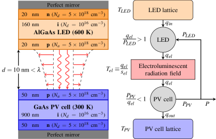
If the conversion efficiency of the PV cell, which can be seen as a heat engine between the EL radiation field and its phonon bath, is high enough, it is then beneficial to take some electrical power from the PV cell back to the LED to enhance the above-bandgap radiation between the two bodies. The below-bandgap radiation remains unchanged, which is essential to keep the PV cell efficiency high. The combination of an LED and a PV cell in such device, as shown in Fig. (1), is called thermophotonics (TPX)Harder and Green (2003). It can be used both as a heat engine and a heat pump/refrigerator. NF effects allowing to reach ELC more easily, it has been combined with the EL enhancement into a NF-TPX deviceZhao et al. (2018); Legendre and Chapuis (2022); Yang et al. (2022). Compared to TPV and NF-TPV, it can be competitive at much lower hot source temperature, down to 450-500 K, and could therefore have applications for low-grade waste heat recovery, as shown in Sec. I of the supplementary material.

In this work, we simulate the performance of a NF-TPX device composed of an AlGaAs PIN LED and a GaAs PIN PV cell (see Fig. (1)). Both the LED and the PV cell are homojunctions.While using heterostructures opens new degrees of freedom for device design, it also comes with its own issues (both in terms of fabrication and physical analysis) and we thus restrict our study to homostructures in the present work. GaAs has been chosen for the PV cell as GaAs-based structures can reach high conversion efficiency, while using AlGaAs for the LED allows to keep the bandgap of both components matched when at different temperatures, maximising the performanceZhao et al. (2018). We place perfect mirror at the back of each component, allowing to improve radiative transfer through cavity effect and preventing radiative losses at the back surface. The impact of mirrors non-ideality on performance was studied by Zhao et al.Zhao et al. (2018).
Modelling such devices requires to couple the resolution of the near-field photon transfer between the two components (LED and PV cell) and of the charge transport in both of them. This resolution is performed in 1D. The near-field radiative heat transfer is obtained using the fluctuational electrodynamics frameworkPolder and Van Hove (1971); Rytov et al. (1989). The spectral photon flux density between any layers i and j is then expressed as:
| (1) |
The total photon and heat flux densities are:
| (2a) | |||
| (2b) | |||
In Eq. (1), corresponds to the difference of the modified Bose-Einstein distribution functions between the two layers, expressed as
| (3) |
where is the photon chemical potential, which accounts for electroluminescent enhancement. It is set to 0 for (no electroluminescence below the bandgap), and can be approximated by above the bandgap. The validity of such approximation for NF-TPV applications was discussed by Callahan et al.Callahan et al. (2021). Here, both components are assumed to be thermal reservoirs, i.e. they remain at constant temperatures. Thus Bose-Einstein distributions are uniform throughout each component, and only above-bandgap photons impact the electrical power generated or consumed.
The second factor in Eq. (1), , corresponds to the photon transmission function, and is obtained through the calculation of the electromagnetic transmission coefficient following Francoeur et al.Francoeur et al. (2009):
| (4) |
The use of such formalism allows to account for frustrated modes (i.e., propagative modes in the components which are tunnelling through the vacuum gap) and surface modes (e.g., surface plasmon polaritons and surface phonon polaritons, which are propagating along interfaces), which enhance the radiative heat transfer in the near field.
The photon flux density being known, the current-voltage (IV) characteristic of each component should be computed. To do so, Poisson (Eq. (5)), drift-diffusion (Eq. (6)) and continuity (Eq. (7)) differential equations are solved in the LED and in the PV cell:
| (5) |
| (6a) | |||
| (6b) | |||
| (7a) | |||
| (7b) | |||
corresponds to the amplitude of the electric field, to the static dielectric constant, (resp. ) to the electron (resp. hole) density, (resp. ) to the donor (resp. acceptor) doping level, to the current density and (resp. ) to the electron (resp. hole) mobility, and should not be confused with the chemical potential. (resp. ) is the closely-related electron (resp. hole) diffusion coefficient, obtained using Einstein’s relation. (resp. ) is the electron-hole pair (EHP) generation (resp. recombination) rate. To account for near-field effects, we assume that the radiative recombination rate equals the above-bandgap (subscript a) emission rate towards the other component, which gives, with Shockley-Read-Hall (SRH) and Auger non-radiative processes:
| (8a) | |||
| (8b) | |||
| (8c) | |||
This neglects the effect of photon recycling on radiative generation and recombination rates. Since and are considered constant in a component, the net internal photon flux (and thus the radiative rate related to photon recycling) should be null.
In a previous paperLegendre and Chapuis (2022), we solved a simplified version of this system of coupled and nonlinear equations, with an assumption that restricts the doping levels to large values and cannot handle PIN junctions. Here, we choose to fully solve it, following Gummel’s iterative methodGummel (1964) and its application to TPV by Blandre et al.Blandre et al. (2017) (see Sec. III of supplementary material for more information on the charge carrier transport model). At boundaries (), we assume that charge neutrality holds (), that majority carriers are at equilibrium (e.g., ) and that minority carriers recombine following a mechanism similar to SRH, e.g. for electrons:
| (9) |
where , are the electron and hole effective surface recombination velocities, and are taken equal to 100 . A similar expression is used for minority holes. The main material properties given as inputs of the simulations can be found in Table 1. Since the variation of non-radiative recombination coefficients with temperature and alloy fraction are currently unknown, they are assumed equal to those of GaAs at 300 K. We only account for alloy-fraction variation in the effective masses.
| Parameter | Symbol | Value | Ref. |
|---|---|---|---|
| Dielectric function | |||
| - Reststrahlen | Adachi (1994); Losego et al. (2009) | ||
| - Interband | Gonzalez-Cuevas et al. (2007) | ||
| Bandgap energy | 1.426 eV | Gonzalez-Cuevas et al. (2007) | |
| e/h rel. eff. mass | Levinshtein et al. (1999) | ||
| e/h mobility | Sotoodeh et al. (2000) | ||
| SRH recomb. coeff. | Sadi et al. (2019) | ||
| Auger recomb. coeff. | Sadi et al. (2019) |
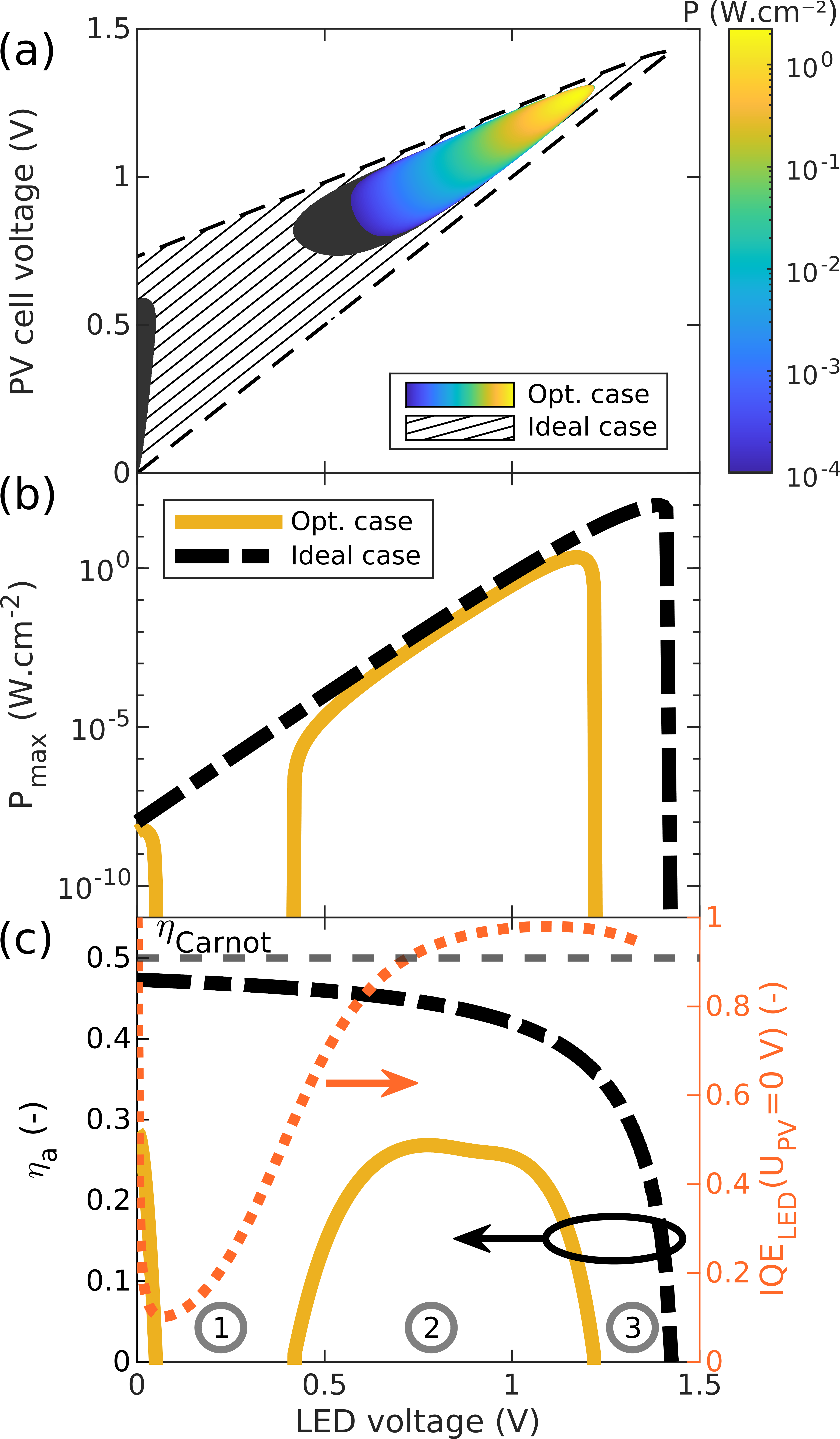
The device considered is shown in Fig. (1), and the thickness and doping level of each layer was obtained through an optimisation process performed at nm and . The optimised device performance is represented in Fig. (2) (in colour). It is compared to the results obtained with an ideal 0D charge carrier transport model (in black), where non-radiative recombinations (both in bulk and at interfaces) are neglected and both components are semi-infinite. Such model has already been extensively used for TPX Harder and Green (2003); Zhao et al. (2018); Legendre and Chapuis (2022). In Fig. (2a), the full power-voltage TPX characteristic is shown, which can be simplified into Fig. (2b) by taking for each LED voltage the maximum power output reached for the given PV cell voltage range. In Fig. (2c), a similar approach is used to obtain the variation of the maximum above-bandgap efficiency with the LED voltage, in which below-bandgap heat transfer is not considered to emphasise the heat-to-electricity conversion. It is expressed as (see Fig. (1) for definitions of the quantities), where is, in fact, really close to the efficiency of the maximum power points found in Fig. (2b), with 1 to 2% absolute difference.


This device is capable of producing electrical power at a rate of with an above-bandgap efficiency of around 13%, and can deliver decent amount of power (up to ) with an efficiency exceeding 25%. This maximum power output is similar to the results obtained in other articles with a 0D charge transport model where surface recombinations are neglected (but accounting for bulk non-radiative losses), with two different set of materials (AlGaAs-GaAsZhao et al. (2018), CdTe-InPYang et al. (2022)). The large power output reached here also overcomes the performance obtained in our previous paper using a simplified 1D charge transport model without surface recombinationsLegendre and Chapuis (2022): using optimised PIN junctions allows to reach similar or higher capabilities, in more realistic conditions.
The variations of the power output with voltages obtained are different to previous TPX results. Usually, the power output increases exponentially with the LED voltage, as for the ideal case in Fig. (2b). The power production region is delimited by a conical shape (as in Fig. (2a)), whose size depends on the significance of the losses taken into account.Legendre and Chapuis (2022). In the considered case however, we see large non-monotonic variations in the low-voltage region, in which the device is not capable of producing power. The study of the LED bulk Internal Quantum Efficiency (IQE), defined as the fraction of radiative recombinations over total bulk recombinations and shown in Fig. (2c), provides a hint about the underlying physics. Indeed, IQE shows similar trends compared to the power output, and forcing it to 1 gives back the usual exponential increase. This means that the performance deterioration at low LED voltage is caused by high non-radiative recombination rates.
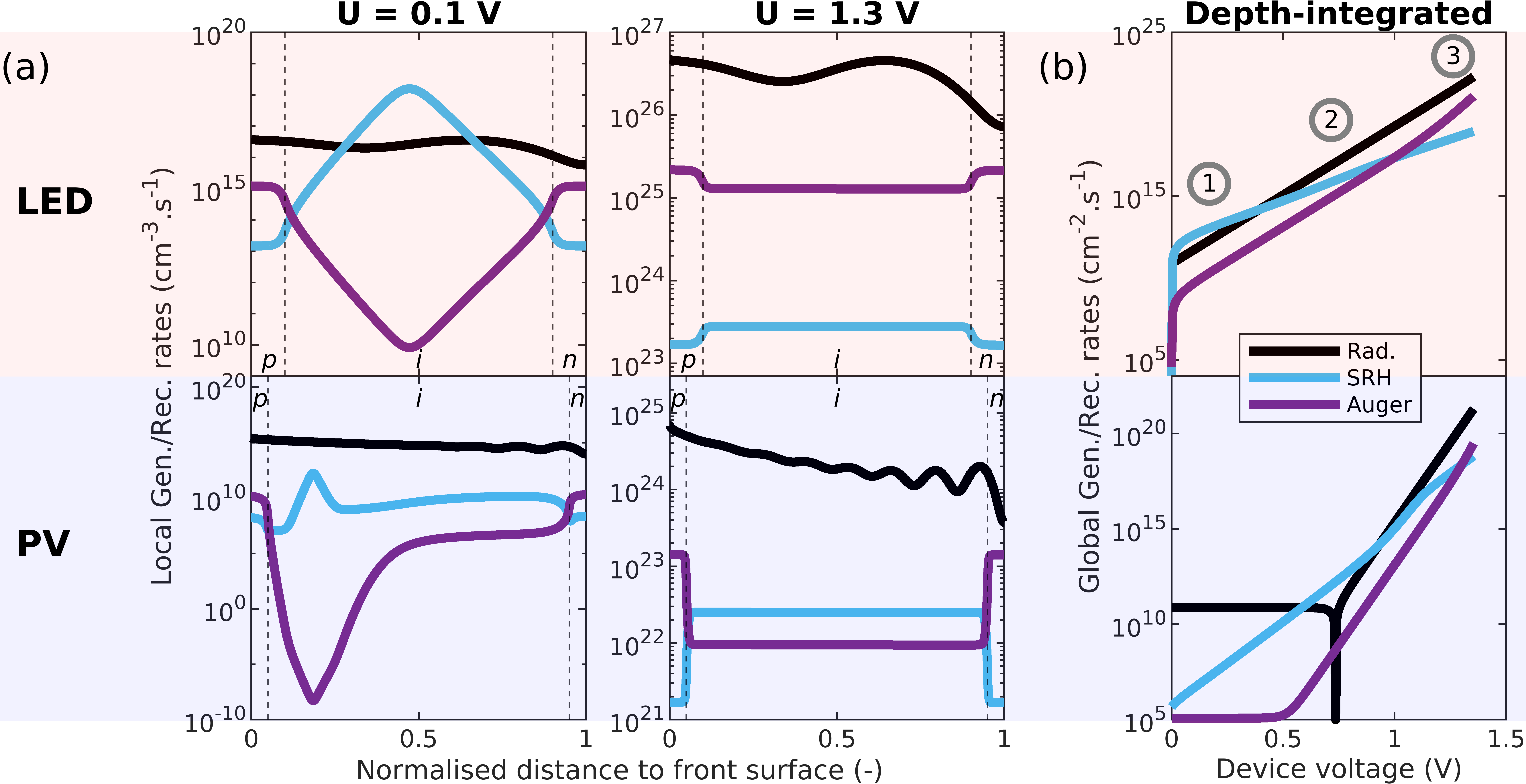
To analyse this in details, we examine the dependence of SRH and Auger recombinations rates with position and voltage. These results can be found in Fig. (3), and are compared with the net radiative generation-recombination rate (which corresponds to the first term on the right of Eq. (8a)). This study is performed for the LED and the PV cell at two different voltages in Fig. (3a), while keeping the opposite component unbiased. In the low-bias case, SRH recombination rates are maximum in the intrinsic layer and minimum in the doped layers, while the opposite is observed for Auger recombinations. This is still true under high bias, however their profile is much more flattened in the i-region, which is due to lower variations in the charge carrier concentrations (see Fig. (S4) in supplementary material, Sec. III). More importantly, the dependence of SRH and Auger recombination rates with voltage are different, Auger recombinations being for instance dominant in the LED i-region at high voltage while negligible at low voltage. This is summarised in Fig. (3b), where the variation with voltage of the quantities integrated over the thickness is shown in absolute value. While the radiative and Auger contributions have similar variations up to high voltage, the SRH one increases with a smaller rate, which is well-known for semiconductor devices (visible for instance in two-diode modelsWürfel (2005)). In the PV cell, recombinations only have an impact after reaching a certain voltage, since radiative generation exceeds them under low bias (corresponding to the region where the radiative and Auger terms are flat in Fig. (3b)). However, their effect is significant at any voltage in the LED in which radiative generation is generally negligible - the component works close to dark conditions. Therefore, three main regions can be delimited for the LED, as shown in Fig. (2c) and (3b). In the first, because SRH lifetimes are not high enough, SRH processes dominate recombinations at low voltage and make the IQE really low. In the second, the highest IQE is reached due to lower increase rate of SRH and moderate Auger recombinations. In the third the latter starts to be dominant, causing a decrease of IQE. The issue for TPX devices is that for small LED IQE, the LED is too inefficient to counterbalance the losses in the PV cell. Then, the device cannot produce power anymore: this is what happens between 0.1 and 0.4 V. Such feature was not observed in previous papers. For the ones using 0D modelsZhao et al. (2018); Yang et al. (2022), SRH recombination lifetimes considered were high, Yang et al. even stating that SRH recombinations were negligible in their case. In our previous paperLegendre and Chapuis (2022), the high doping levels limited the SRH recombination rate.

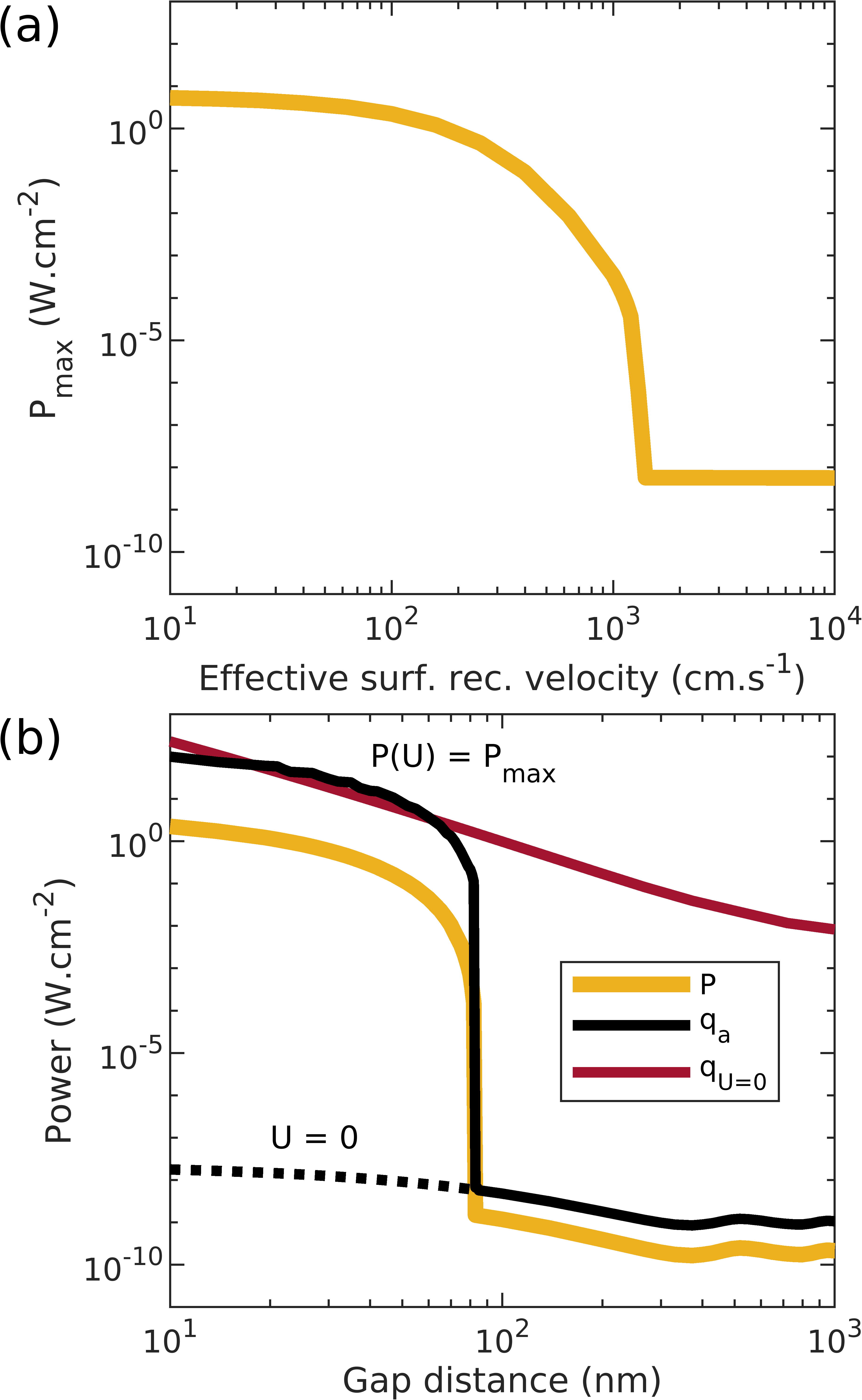
The large amount of SRH recombinations at low voltage comes from the significant thickness of the i-region in both components, in which they exceed Auger recombinations as seen in Fig. (3a). In return, it allows to limit Auger recombinations at high voltage and thus to perform better. However, this non-monotonic behaviour will have a large impact if the working conditions are changed. This is shown in Fig. (4), where the effective surface recombination velocity S and the gap distance d are changed for the given device. Similar trends can be observed for both. While previous papers reported a smooth decrease of the performance with the gap distanceZhao et al. (2018); Legendre and Chapuis (2022), the power output drops dramatically when using the considered device, respectively around and 100 nm. Indeed, increasing one of these quantities decreases the LED WPE. This is due either to a quicker decrease of the radiative term (directly related to ) compared to the non-radiative ones (indirectly related to via the carrier concentrations) or to an increase of interface losses. As explained previously, this decreases the region in which the TPX device can deliver power, up to the point where it is no longer beneficial to bias the LED. Then the optimal case is close to TPV (almost no LED bias), as commented in Sec. II of supplementary material. For the device considered, near-field effects are thus necessary to make the thermodynamic machine work, and cannot be interpreted as a bonus to add on top of TPX performance (as it is the case for TPV).
We now study the impact of the gap distance on the total radiated heat flux. While for the gap distances considered, mainly frustrated modes intervene for interband transitions, surface modes are important below the bandgap due to surface phonon and plasmon polaritons. As a consequence, without electroluminescent amplification, the total heat flux increases quicker than the above-bandgap heat flux when the gap distance decreases. In parallel, the above-bandgap heat flux jumps around 100 nm thanks to electroluminescence. Because of these two phenomena, the fraction of radiation located above the bandgap reaches a maximum of 65% around 35 nm, and goes down to 30% at 10 nm gap distance. The full device efficiency can also be computed, and is of course lower compared to its above-bandgap equivalent because of below-bandgap photons. It is equal to 2.4% at 35 nm, and to 0.92% at 10 nm. The complete variations of these quantities with the gap distance are shown in Sec. II of supplementary material (see Fig. S3). While these values are low, it should be possible to partially suppress the below-bandgap resonances, for instance with the use of Pt thin filmsYang et al. (2022). This would help to come closer to the above-bandgap efficiency, and limit the heat extraction issue.
In summary, the performance of an AlGaAs-GaAs NF-TPX device was simulated using fluctuational electrodynamics and an iterative resolution of Poisson, continuity and drift-diffusion equations in 1D. Compared to 0D or simplified 1D models, the study of more complex structures becomes achievable, in particular when made of weakly-doped or intrinsic layers. The realistic device considered reaches a power production of with an above-bandgap efficiency of 13% at a 10 nm gap distance. The use of PIN homojunctions allows to increase the device performance through the limitation of Auger recombination losses and shines a light on the drastic impact of SRH recombinations on TPX characteristic at low voltage. In order to obtain even better capabilities, heterojunctions are attractive due to their high carrier selectivity and the possibility to suppress SRH recombinations through fine control of the doping profileSanthanam et al. (2020).
Supplementary material
See supplementary material for a comparison of NF-TPX with other technologies, a more detailed analysis of the gap distance influence, and a description of the charge carrier transport model used.
Acknowledgements
The project TPX-Power has received funding from the European Union’s Horizon 2020 research and innovation programme under grant agreement No. 951976. We thank P. Kivisaari and J. van Gastel for the useful discussions.
Author declarations
Conflict of interest
The authors have no conflicts to disclose.
Data availability
The data that support the findings of this study are available from the corresponding author upon reasonable request.
References
- Mao et al. (2018) J. Mao, Z. Liu, J. Zhou, H. Zhu, Q. Zhang, G. Chen, and Z. Ren, Advances in Physics 67, 69 (2018).
- Campbell et al. (2021) M. F. Campbell, T. J. Celenza, F. Schmitt, J. W. Schwede, and I. Bargatin, Advanced Science 8, 2003812 (2021).
- LaPotin et al. (2022) A. LaPotin, K. L. Schulte, M. A. Steiner, K. Buznitsky, C. C. Kelsall, D. J. Friedman, E. J. Tervo, R. M. France, M. R. Young, A. Rohskopf, S. Verma, E. N. Wang, and A. Henry, Nature 604, 287 (2022), arXiv:2108.09613 .
- Green and Bremner (2016) M. A. Green and S. P. Bremner, Nature Materials 16, 23 (2016).
- Inoue et al. (2021) T. Inoue, K. Ikeda, B. Song, T. Suzuki, K. Ishino, T. Asano, and S. Noda, ACS Photonics 8, 2466 (2021).
- Lucchesi et al. (2021) C. Lucchesi, D. Cakiroglu, J.-P. Perez, T. Taliercio, E. Tournié, P.-O. Chapuis, and R. Vaillon, Nano Letters 11, 4524 (2021).
- Mittapally et al. (2021) R. Mittapally, B. Lee, L. Zhu, A. Reihani, J. W. Lim, D. Fan, S. R. Forrest, P. Reddy, and E. Meyhofer, Nature Communications 12, 4364 (2021).
- Song et al. (2022) J. Song, J. Han, M. Choi, and B. J. Lee, Solar Energy Materials and Solar Cells 238, 111556 (2022).
- Okanimba Tedah et al. (2019) I. A. Okanimba Tedah, F. Maculewicz, D. E. Wolf, and R. Schmechel, Journal of Physics D: Applied Physics 52, 275501 (2019).
- Volokitin and Persson (2007) A. I. Volokitin and B. N. Persson, Reviews of Modern Physics 79, 1291 (2007).
- Santhanam et al. (2012) P. Santhanam, D. J. Gray, and R. J. Ram, Physical Review Letters 108, 1 (2012).
- Radevici et al. (2019) I. Radevici, J. Tiira, T. Sadi, S. Ranta, A. Tukiainen, M. Guina, and J. Oksanen, Applied Physics Letters 114, 051101 (2019).
- Sadi et al. (2020) T. Sadi, I. Radevici, and J. Oksanen, Nature Photonics 14, 205 (2020).
- Weinstein (1960) M. A. Weinstein, Journal of the Optical Society of America 50, 597 (1960).
- Landsberg and Evans (1968) P. T. Landsberg and D. A. Evans, Physical Review 166, 242 (1968).
- Xue et al. (2017) J. Xue, Z. Li, and R. J. Ram, Physical Review Applied 8, 014017 (2017).
- Harder and Green (2003) N. P. Harder and M. A. Green, Semiconductor Science and Technology 18, S270 (2003).
- Zhao et al. (2018) B. Zhao, P. Santhanam, K. Chen, S. Buddhiraju, and S. Fan, Nano Letters 18, 5224 (2018).
- Legendre and Chapuis (2022) J. Legendre and P.-O. Chapuis, Solar Energy Materials and Solar Cells 238, 111594 (2022).
- Yang et al. (2022) F. Yang, K. Chen, Y. Zhao, S.-K. Kim, X. Luo, and R. Hu, Applied Physics Letters 120, 053902 (2022).
- Polder and Van Hove (1971) D. Polder and M. Van Hove, Physical Review B 4, 3303 (1971).
- Rytov et al. (1989) S. M. Rytov, Y. A. Kravtsov, and V. I. Tatarskii, Principles of Statistical Radiophysics, Vol. 3 (Springer Berlin, Heidelberg, 1989).
- Callahan et al. (2021) W. A. Callahan, D. Feng, Z. M. Zhang, E. S. Toberer, A. J. Ferguson, and E. J. Tervo, Physical Review Applied 15, 054035 (2021).
- Francoeur et al. (2009) M. Francoeur, M. Pinar Mengüç, and R. Vaillon, Journal of Quantitative Spectroscopy and Radiative Transfer 110, 2002 (2009).
- Gummel (1964) H. K. Gummel, IEEE Transactions on Electron Devices 11, 455 (1964).
- Blandre et al. (2017) E. Blandre, P.-O. Chapuis, and R. Vaillon, Scientific Reports 7, 15860 (2017).
- Adachi (1994) S. Adachi, GaAs and Related Materials (World Scientific, 1994) p. 696.
- Losego et al. (2009) M. D. Losego, A. Y. Efremenko, C. L. Rhodes, M. G. Cerruti, S. Franzen, and J. P. Maria, Journal of Applied Physics 106, 024903 (2009).
- Gonzalez-Cuevas et al. (2007) J. A. Gonzalez-Cuevas, T. F. Refaat, M. N. Abedin, and H. E. Elsayed-Ali, Journal of Applied Physics 102, 014504 (2007).
- Levinshtein et al. (1999) M. E. Levinshtein, S. Rumyantsev, and M. Shur, Handbook Series on Semiconductor Parameters, Vol. 2—Ternary and Quaternary III-V Compounds (World Scientific, 1999).
- Sotoodeh et al. (2000) M. Sotoodeh, A. H. Khalid, and A. A. Rezazadeh, Journal of Applied Physics 87, 2890 (2000).
- Sadi et al. (2019) T. Sadi, I. Radevici, P. Kivisaari, and J. Oksanen, IEEE Transactions on Electron Devices 66, 2651 (2019).
- Würfel (2005) P. Würfel, Physics of Solar Cells (Wiley, 2005) p. 274.
- Santhanam et al. (2020) P. Santhanam, W. Li, B. Zhao, C. Rogers, D. J. Gray, P. Jahelka, H. A. Atwater, and S. Fan, Applied Physics Letters 116, 203503 (2020).