Fully-Binarized, Parallel, RRAM-based Computing Primitive for In-Memory Similarity Search
Abstract
In this work, we propose a fully-binarized XOR-based IMSS (In-Memory Similarity Search) using RRAM (Resistive Random Access Memory) arrays. XOR (Exclusive OR) operation is realized using 2T-2R bitcells arranged along the column in an array. This enables simultaneous match operation across multiple stored data vectors by performing analog column-wise XOR operation and summation to compute HD (Hamming Distance). The proposed scheme is experimentally validated on fabricated RRAM arrays. Full-system validation is performed through SPICE simulations using open source Skywater 130 nm CMOS PDK demonstrating energy of 17 fJ per XOR operation using the proposed bitcell with a full-system power dissipation of 145 W. Using projected estimations at advanced nodes (28 nm) energy savings of 1.5 compared to the state-of-the-art can be observed for a fixed workload. Application-level validation is performed on HSI (Hyper-Spectral Image) pixel classification task using the Salinas dataset demonstrating an accuracy of 91%.
Index Terms:
RRAM, In-Memory Computing, Similarity Search, Edge-AI, Low-power computingI Introduction
Associative memories (or CAM - Content Addressable Memory) are an important component of intelligent systems that can perform fast search operations [1]. CAMs accept a query and perform search over multiple data points stored in memory to find one or more matches based on a distance metric and return locations of matches. This information can be potentially used for applications such as nearest neighbour searches for classification or unsupervised labeling[2, 3, 4, 5]. One of the basic distance metrics that can be used for such applications is HD (Hamming Distance)[2]. For any pair of strings or words of equal length, HD is defined as the total number of positions where the symbols/characters of the pair differ from each other. Conventional CAMs are designed using standard memory technologies such as SRAM (16T [6], 9T NOR-based and 10T NAND-based bitcells [7]) or DRAM [8, 9]. However, such volatile memory-based circuits have performance limitations that can be potentially addressed by using emerging NVM (Non-Volatile Memory) devices[10, 11, 12]. Use of NVM devices provides additional design flexibility by reducing circuit complexity and providing opportunity to exploit low-area analog IMC (In-Memory Computing)[10, 13]. Associative memory architectures that exploit NVM based IMC have been recently demonstrated using RRAM (Resistive RAM) devices based on XNOR[14, 15, 16, 17, 5, 1] and XOR[3, 18] logic using HD as the distance metric. In this work, an end-to-end scheme is proposed to realize IMSS (In-Memory Similarity Search) in hardware by using RRAM devices and binarizing data and queries through a custom pre-processing pipeline. XOR gate functionality is realized using 2T-2R RRAM circuits where one input is encoded in form of RRAM device conductance states and the other input is applied as voltage signals. Reasons for adopting the 2T-2R bitcell for the study are: (i) Improved tolerance for D2D (Device-to-Device)/C2C (Cycle-to-Cycle) variability compared to 1T-1R resulting in reliable operations even at relaxed programming conditions potentially increasing endurance[19]; (ii) Improved resilience to impact of resistance drift or read-disturbs for the programmed states and (iii) High signal margins easing the sensing requirements[17].
© 2022 IEEE. Personal use of this material is permitted. Permission from IEEE must be obtained for all other uses, in any current or future media, including reprinting/republishing this material for advertising or promotional purposes, creating new collective works, for resale or redistribution to servers or lists, or reuse of any copyrighted component of this work in other works.
In an array structure when such circuits are arranged in column-orientation, QI (Query Input) can be simultaneously applied to multiple columns of SD (Stored Data). Key contributions of the work are: (i) Experimental validation of 2T-2R XOR bitcell operation on fabricated 88 1T-1R RRAM arrays, (ii) Scheme for performing fully-binarized XOR-based IMSS through analog computation of HD, (iii) Validation of IMSS peripheral circuits through detailed SPICE simulations using 130 nm Skywater PDK, (iv) Validation of proposed methodologies on HSI (Hyper-Spectral Image) classification application with Salinas dataset and (v) Analysis depicting impact of array size on sensing margin and variability on classification accuracy. The manuscript is organized as follows: Section II summarizes the RRAM device fabrication flow. Section III presents the experimental validation of proposed RRAM IMSS scheme. Section IV presents the SPICE simulation results for IMSS architecture considering the periphery blocks. Section V presents the application level validation of the proposed IMSS scheme on HSI pixel classification task using the Salinas dataset and finally Section VI provides concluding remarks.
II Fabricated RRAM Array
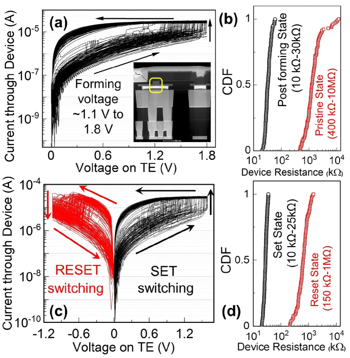
The fabricated test chip used in our study is of size 16kb consisting of 256 88 1T-1R RRAM arrays [20]. The SEM cross-section of fabricated RRAM device integrated on top of 130 nm CMOS technology is shown in the inset of Fig. 1(a). The device stack has TiN as BE (Bottom Electrode), non-stoichiometric SiOx as switching layer and TiN as TE (Top Electrode). The 1T-1R bitcell occupies 30F2 on-chip area. Fig. 1(a,b) shows the electro-forming characteristics (where an initial conductive filament is formed) and cumulative distribution for pristine- and post-forming device resistance (in k). Fig. 1(c) shows SET and RESET switching characteristics highlighting D2D variability for the 88 RRAM device array. LRS (Low Resistance State) and HRS (High Resistance State) device resistance distributions are shown in Fig. 1(d). It is observed that the LRS ranges from 3 k to 20 k and HRS ranges from 110 k to 1 M.
III RRAM IMSS: Experiments and Working
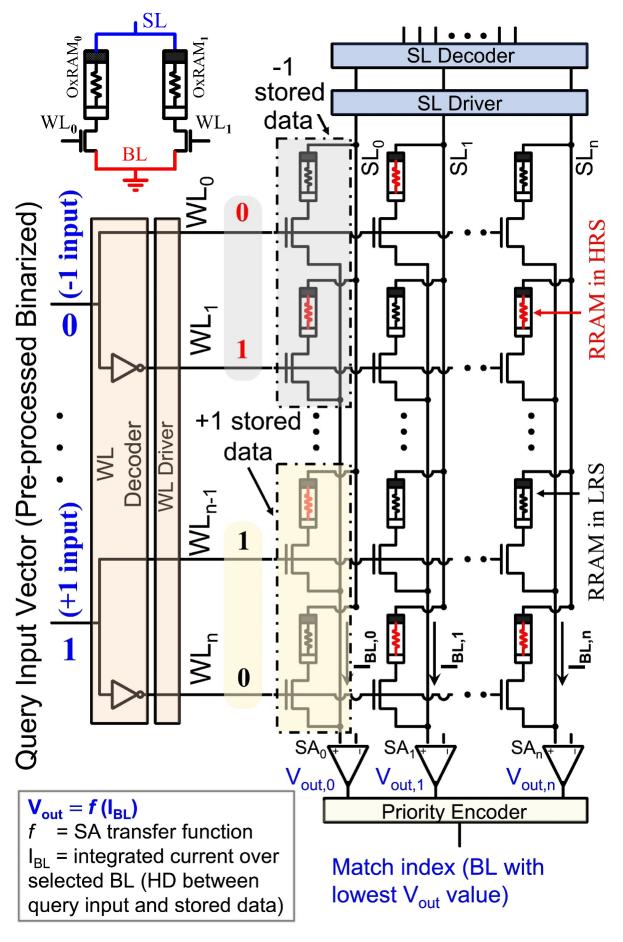
Schematic representation of 88 1T-1R RRAM array used for experimental validation is illustrated in Fig. 2. To access a desired memory bitcell, the row address is selected by enabling corresponding WL and column address by selecting BL/SL. Data vectors are stored in the form of RRAM device conductance along columns (‘-1’ is encoded as top RRAM = LRS, bottom RRAM = HRS. While ‘+1’ is encoded as top RRAM = HRS, bottom RRAM = LRS). For programming RRAM to LRS, 1 s long SET pulse is applied with VWL=1.8 V, VSL=1.4 V and VBL=0 V. For HRS, 1 s RESET pulse is applied with VWL=4.5 V, VSL=0 V and VBL=1.2 V. To read bitcell resistance, a 50 s READ pulse with VWL=1.4 V, VSL=0.2 V and VBL=0 V is applied. For realizing a XOR gate in hardware, a 2T-2R bitcell is effectively realized by selecting two consecutive 1T-1R bitcells in the same column. QI is applied in binary format (‘-1’,‘+1’). To eliminate the need for negative voltage (i.e., to represent ‘-1’), binary input is converted to a differential representation: ‘-1’ [0,1], and ‘+1’ [1,0] using a WL-decoder circuit. To perform XOR operation, SL is charged to 0.2 V and QI is applied as input to corresponding 2T-2R bitcell. Output of the circuit is obtained in the form of current flowing through corresponding BL. When the QI matches SD, RRAM in HRS is selected and negligible current flows. In case of a mismatch, RRAM in LRS is selected leading to higher output current. For a single column, output current of all XOR cells can be integrated following the principle of KCL (Kirchoff’s Current Law) representing the HD between QI and SD as shown below in Eq. (1).
| (1) |
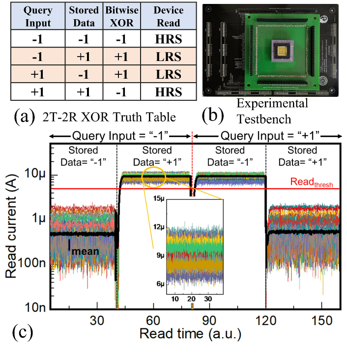
Fig. 3(a) presents the truth table validating XOR gate functionality. In addition to XOR circuit functionality, the proposed scheme also improves robustness to programming errors as opposed to a single 1T-1R bitcell[19] due to differential storage. Fig. 3(b) shows the custom experimental setup and RRAM test chip used in the study. Programming signals are applied using high speed pulse measurement unit (Keithley 4225-PMU) from semiconductor parameter analyzer (Keithley 4200-SPA). The signals from PMU channels are multiplexed and applied to different signal lines (WL,SL,BL) using the custom switch board. Experimental validation of a single 2T-2R bitcell based XOR gate for all possible input combinations across 32 2T-2R XOR bitcells is presented in Fig. 3(c). Average (Read Current) is found to be less than 1 A (i.e. RRAM device in HRS gets selected) when QI matches SD. When QI doesn’t match SD i.e mismatch, average is 6 A (i.e. RRAM device in LRS gets selected). A reliable sense-margin 5A is realized between match and mismatch states. For a given QI vector, the current will be the lowest through BL storing match/nearest match data vector. To perform IMSS, = 0.2 V is applied on SLs with SD vectors to be compared against applied QI vector. HD is computed by applying an n-bit long binary QI vector and comparing it against n-bit binary SD vectors; at each SL, there are n 2T-2R XOR gates participating. Bit level comparison is carried out by each XOR gate and summed up IBL (Bit-line Current) from n XOR gates is sensed on corresponding BL. BL/SL with maximum match bits will result in the lowest current. IBL is converted to Vout (voltage sensed by SA (Sense Amplifier)).
IV SPICE Simulations
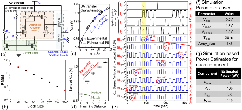
To validate the proposed IMSS architecture, SPICE simulations using the Opensource Skywater 130 nm PDK[21] are performed with ngspice. Simulations included RRAM arrays (modeled through resistance matrices) and periphery circuits shown in Fig. 2 and Fig. 4(a). Decoder-circuit/logic blocks and SA-circuits are designed with =1.4 V and 1.8 V respectively. Experimentally measured resistance values of LRS/HRS are used for the 1T-1R array during simulations. Transfer curve for the SA used in the simulation analysis is shown in Fig. 4(c). Gain of SA is selected based on length of the column vector so that full-mismatch leads to Vout VDD and full-match leads to Vout 0 V. Vout as a function of HD, between a 4-bit QI vector and a 4-bit SD vector is shown in Fig. 4(d). Timing waveform showcasing all possible QI vector combinations and SA outputs for a 48 2T-2R array are shown in Fig. 4(e). Vout is minimum when QI vector matches the SD vector. For instance, when applied QI is “0100”, Vout for BL7 is minimum because the SD along BL7 is “0100”. After incorporating measured D2D variability (Fig. 1(b),(d)) in the simulations, the proposed IMSS scheme shows no overlap between output voltage levels for neighbouring HD values thus demonstrating a reliable operation. To estimate energy dissipation, current waveforms for all supply voltages (, , ) over a set of 32 input combinations were obtained through simulations. The simulations utilized a clock of 50 MHz. Based on average current dissipation for all operations, average power was estimated. Total power dissipation was estimated to be 145 W with energy cost per XOR operation of 17 fJ. A complete breakdown of power estimation is shown in Fig. 4(g) with methodology for estimation explained in Eq. (2)-(3). In this study, we have exclusively focused on array size = 88 in order to align with experimental measurements. However, array size has a significant contribution in determining overall performance for the IMC arrays[20]. For a constant workload, with increase in array size latency would decrease due to reduction in number of operation. However the cost of a single operation increases due to periphery overhead. Additionally increasing array size may lead to limitations in terms of sensing margin (see Fig. 4(b)).
| (2) | ||||
| (3) |
| Ref. | Device | Set | Reset | Read | (pJ) | Tech. | Array | Application | Dataset |
|---|---|---|---|---|---|---|---|---|---|
| Stack | Pulse | Pulse | Pulse | (12832) | Node | ||||
| This | 2V, 1s | -1.4V, 2s | 0.2V, 20ns | 71.26 | 130 nm | 16 kB | Similarity Search | Salinas | |
| work | Si-doped [22] | 2.7V, 1s | -2.7V, 1s | 0.1V, 10ns | 28.67 | 28 nm | |||
| [5] | 3.3V, 1s | -3.5V, 100s | 0.2V, 10ns | 42.76 | 40 nm | 64 kB | One-shot learning | Omniglot | |
| [17] | Tran. + | 2V, 0.2s | -3V, 0.2s | 50mV, 100ns | 0.82 | 90 nm | Sim. | Similarity Search | NA |
| [23] | 2V, 0.1s | -2.5V, 0.1s | 0.6V, 90ns | 44.46 | 130 nm | 4 kB | NA | NA | |
| [16] | FeFET | -4V, 10s | 4V, 10s | 1V, 1ns | 4.62 | 45 nm | Sim. | One-shot learning | Omniglot |
| [15] | PCM | 2.5V,10ns | 1.2V, 1.9ns | 32.13 | 90 nm | 1 Mb | Similarity Search | NA | |
| [14] | MRAM | 50A | -150A | 1.5V | NA | 140 nm | 9kb | Similarity Search | NA |
V HSI Classification Task
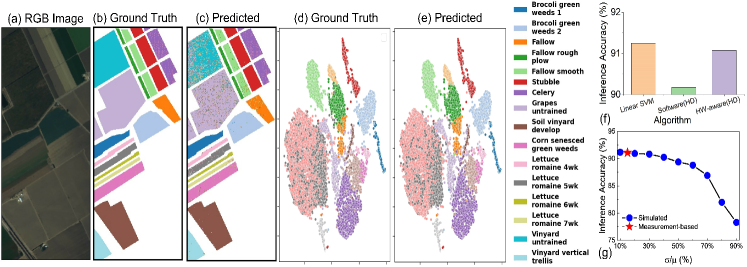
HSI classification on the ‘Salinas’ dataset is used as an example usecase for the proposed IMSS architecture where every pixel in the image is classified to identify the type and age of the vegetation present on ground. Dataset includes HSI of size 512217 with 224 bands acquired using AVIRIS (Airborne Visible/Infrared Imaging Spectrometer) [24] sensor flying over Salinas Valley, California. RGB representation of the image is shown in Fig. 5(a). Ground truth comprises of 16 types of vegetation classes (see Fig. 5(b)). Design of HSI application-specific pre-processing pipeline becomes essential in order to obtain a simplified representation of the data without losing information. In case of HSI since both data precision and spectral resolution is high, compression becomes important. Custom pre-processing steps used for performing IMSS using Salinas dataset are summarized in Algorithm 1. First step involves performing PCA (Principal Component Analysis) [25] to extract relevant feature data, followed by log-scaling to compress data representation especially in case of large integers. To preserve the dynamic range, sign-multiplication is performed followed by normalization using two methods: mean-sigma followed by min-max. At the final step, 8-bit unsigned integer (uint8) representation is created. In the proposed HSI classification pipeline, use of only XOR operations is ensured to exploit the 2T-2R IMC array. Due to position specific weight assigned to each bit in case of fixed-point numbers, directly computing HD may lead to inaccurate match operation. To overcome this issue, uint8 values are converted to an 8-bit thermometric encoding [26] with a resolution of 32. This facilitates assigning equal numerical significance to each bit thus making HD a feasible metric for performing IMSS operation. Using the aforementioned pre-processing pipeline, input HSI data is compressed to 20 channels where each channel is translated to 8 channels of binary thermometric encoding. Each pixel in the original image is stored as a 160 bit vector (208) i.e. compression by a factor of 44. For training, 70% of the dataset (image pixels) is used. Entire training data, based on the proposed differential encoding scheme, would require an RRAM IMSS chip (Fig. 2) of size 24MB. Since this requires a modest chip size for high-density RRAM, software simulations were performed using the PyTorch framework to validate the full Salinas classification application based on proposed RRAM IMSS. Pre-processed feature vectors from the test set are applied as QI to compute HD through XOR operations between SD vector and QI vector. Index of the SD vector with least distance is computed and class label from corresponding index is assigned to the test vector. Inference results using proposed IMSS scheme are shown in Fig. 5(c). To visualize learning performance in form of 2D-decision spaces, t-SNE (t-Distributed Stochastic Neighbour Embedding) [27] plots are generated for both ground-truth and predicted results as shown in Fig. 5(d) and Fig. 5(e) respectively. A comparison of the proposed HW-based approach against standard classification algorithms and software-based realization is shown in Fig. 5(f). For HW-aware simulations we incorporate the experimentally measured D2D variability of individual resistance states as shown in Fig. 1(d). To further demonstrate the resilience benefits of the 2T-2R structure, inference accuracies were estimated by sweeping the device variability for both HRS and LRS states simultaneously (see Fig. 5(g)). Table I presents comparison with other RRAM-based IMSS studies in literature. The proposed methodology enables simultaneous processing of 8 rows to determine HD as opposed to prior work where only 4 rows can be sensed in a single cycle of operation[5]. This however comes at the cost of increased energy dissipation from the SA circuit. When comparing device read energy costs for processing IMSS across 32 vectors of 128-bit, it can be observed that current implementation consumes 2 more energy compared to state-of-the-art array-based implementations. For the case of FeFET and MoS2 transistor-based realizations, the array structures have been realized in simulation and hence haven’t been considered for comparison. However, projected estimations using parameters from a 28 nm fabricated 1T-1R arrays[22] demonstrates energy savings of 2.5 compared to present implementation and 1.5 compared to SOTA IMC bitcells.
VI Conclusion
Successful realization of XOR operations based on 2T-2R circuits using fabricated RRAM was experimentally validated. Analog computation of HD based on column-wise current integration to perform binarized IMSS was realized through extensive SPICE simulations including peripheral circuits using the Skywater 130 nm PDK. Simulations validated energy of 17 fJ per XOR operation with a full-system power dissipation of 145 W for 88 RRAM array. Using projected estimations at advanced nodes (28 nm) energy savings of 1.5 compared to the state-of-the-art can be observed for a fixed workload. Proposed IMSS scheme was used for HSI pixel classification demonstrating 91% accuracy.
References
- [1] Y. Pan et al., “A rram-based associative memory cell,” in ISCAS 2021, Daegu, South Korea, May 22-28, 2021. IEEE, 2021, pp. 1–5.
- [2] M. Imani et al., “A binary learning framework for hyperdimensional computing,” in DATE. IEEE, 2019, pp. 126–131.
- [3] T. F. Wu et al., “Hyperdimensional computing exploiting carbon nanotube fets, resistive ram, and their monolithic 3d integration,” IEEE JSSC, vol. 53, no. 11, pp. 3183–3196, 2018.
- [4] M. Imani et al., “Dual: Acceleration of clustering algorithms using digital-based processing in-memory,” in MICRO, 2020, pp. 356–371.
- [5] H. Li et al., “Sapiens: A 64-kb rram-based non-volatile associative memory for one-shot learning and inference at the edge,” IEEE TED, pp. 1–7, 2021.
- [6] N. Mohan et al., “Low-leakage storage cells for ternary content addressable memories,” IEEE TVLSI, vol. 17, no. 5, pp. 604–612, 2009.
- [7] K. Pagiamtzis et al., “Content-addressable memory (CAM) circuits and architectures: a tutorial and survey,” IEEE JSSC, vol. 41, no. 3, pp. 712–727, 2006.
- [8] H. Noda et al., “A cost-efficient high-performance dynamic TCAM with pipelined hierarchical searching and shift redundancy architecture,” IEEE JSSC, vol. 40, no. 1, pp. 245–253, jan 2005.
- [9] V. Lines et al., “66 MHz 2.3 m ternary dynamic content addressable memory,” in Records of the IEEE International Workshop on Memory Technology, Design and Testing. IEEE Comput. Soc, 2000.
- [10] R. Karam et al., “Emerging trends in design and applications of memory-based computing and content-addressable memories,” Proceedings of the IEEE, vol. 103, no. 8, pp. 1311–1330, 2015.
- [11] X. Sun et al., “Xnor-rram: A scalable and parallel resistive synaptic architecture for binary neural networks,” in DATE, 2018, pp. 1423–1428.
- [12] S. Shreya et al., “Energy-efficient all-spin bnn using voltage-controlled spin-orbit torque device for digit recognition,” IEEE TED, vol. 68, no. 1, pp. 385–392, 2021.
- [13] D. Ielmini et al., “In-memory computing with resistive switching devices,” Nature Electronics, vol. 1, no. 6, pp. 333–343, jun 2018.
- [14] S. Matsunaga et al., “Implementation of a perpendicular mtj-based read-disturb-tolerant 2t-2r nonvolatile tcam based on a reversed current reading scheme,” in ASPDAC, 2012, pp. 475–476.
- [15] J. Li et al., “1 mb 0.41 µm² 2t-2r cell nonvolatile tcam with two-bit encoding and clocked self-referenced sensing,” IEEE JSSC, vol. 49, no. 4, pp. 896–907, 2014.
- [16] K. Ni et al., “Ferroelectric ternary content-addressable memory for one-shot learning,” Nature Electronics, vol. 2, no. 11, pp. 521–529, nov 2019.
- [17] R. Yang et al., “Ternary content-addressable memory with MoS2 transistors for massively parallel data search,” Nature Electronics, vol. 2, no. 3, pp. 108–114, mar 2019.
- [18] Y. Halawani et al., “Stateful memristor-based search architecture,” IEEE TVLSI, vol. 26, no. 12, pp. 2773–2780, 2018.
- [19] M. Bocquet et al., “In-memory and error-immune differential rram implementation of binarized deep neural networks,” in IEDM, 2018, pp. 20.6.1–20.6.4.
- [20] S. K. Kingra et al., “Dual-configuration in-memory computing bitcells using siox rram for binary neural networks,” Applied Physics Letters, vol. 120, no. 3, p. 034102, 2022.
- [21] “Skywater open source pdk,” https://github.com/google/skywater-pdk.
- [22] L. Grenouillet et al., “16kbit 1t1r oxram arrays embedded in 28nm fdsoi technology demonstrating low ber, high endurance, and compatibility with core logic transistors,” in IMW, 2021, pp. 1–4.
- [23] D. R. B. Ly et al., “Novel 1t2r1t rram-based ternary content addressable memory for large scale pattern recognition,” in IEDM, 2019, pp. 35.5.1–35.5.4.
- [24] G. Vane et al., “The airborne visible/infrared imaging spectrometer (aviris),” Remote sensing of environment, vol. 44, no. 2-3, pp. 127–143, 1993.
- [25] S. Wold et al., “Principal component analysis,” Chemometrics and intelligent laboratory systems, vol. 2, no. 1-3, pp. 37–52, 1987.
- [26] J. Buckman et al., “Thermometer encoding: One hot way to resist adversarial examples,” in ICLR, 2018, pp. 1–22.
- [27] L. van der Maaten et al., “Visualizing data using t-sne,” JMLR, vol. 9, no. 86, pp. 2579–2605, 2008.