Electric-field induced magnetic-anisotropy transformation to achieve spontaneous valley polarization
Abstract
Valleytronics has been widely investigated for providing new degrees of freedom to future information coding and processing. Here, it is proposed that valley polarization can be achieved by electric field induced magnetic anisotropy (MA) transformation. Through the first-principle calculations, our idea is illustrated by a concrete example of monolayer. The increasing electric field can induce a transition of MA from in-plane to out-of-plane by changing magnetic anisotropy energy (MAE) from negative to positive value, which is mainly due to increasing magnetocrystalline anisotropy (MCA) energy. The out-of-plane magnetization is in favour of spontaneous valley polarization in . Within considered electric field range, is always ferromagnetic (FM) ground state. In a certain range of electric field, the coexistence of semiconductor and out-of-plane magnetization makes become a true ferrovalley (FV) material. The anomalous valley Hall effect (AVHE) can be observed under in-plane and out-of-plane electrical field in . Our works pave the way to design the ferrovalley material by electric field.
I Introduction
The manipulation of the carriers’ properties is key for semiconductor technology. In addition to charge and spin of carriers, the valley, as a new degree of freedom, is characterized by a local energy extreme in the conduction band or valence band. To encode, store and process information, two or more degenerate but inequivalent valley states at the inequivalent points should exist in a materialb1 ; b2 . Since the two-dimensional (2D) materials, especially 2D 2H-phase transition metal dichalcogenides (TMDCs), are booming, the valley-related filed is truly flourishingq8-1 ; q8-2 ; q8-3 ; q9-1 ; q9-2 ; q9-3 ; q9-4 . Nevertheless, realizing the valley polarization is indispensable to achieve valley application. To induce valley polarization, many methods have been proposed, such as optical pumping, magnetic field, magnetic substrates and magnetic dopingq8-1 ; q8-2 ; q8-3 ; q9-1 ; q9-2 ; q9-3 ; q9-4 . However, these methods have some disadvantages that the intrinsic energy band structures and crystal structures can be destroyed. Recently, FV materials have been proposed, which possess intrinsic spontaneous valley polarization introduced by their intrinsic ferromagnetismq10 . The FV materials can overcome these shortcomings of the extrinsic valley polarization materials. Many 2D materials have been predicted to have spontaneous valley polarizationq10 ; q11 ; q12 ; q13 ; q13-1 ; q14 ; q14-0 ; q14-1 ; q14-2 ; q14-3 ; q15 ; q16 ; q17 ; q18 ; q19 .
However, many of predicted 2D FV materials intrinsically have no spontaneous valley polarization, because their magnetization are preferentially in the layer planeq14-1 ; q14-2 ; q14-3 . To achieve valley polarization in these materials, the external magnetic field is needed to adjust magnetization from in-plane to out-of-plane. Even though predicted 2D FV material possesses out-of-plane magnetization, the MAE is calculated with only considering MCA, not including magnetic shape anisotropy (MSA). For example, the easy magnetization axis of is in-plane orientation with including MSAgsd , which is different from previous out-of-plane one with only considering MCA energyq14 . Thus, MSA is very important to determine MA of 2D materials with weak spin-orbital coupling (SOC), like the representative 2D magnet with an easy in-plane magnetization in experimenta1-3 ; a1-4 . Only considering MCA energy shows an easy out-of-plane magnetization for , but the theoretical results with including MSA energy agree well with experimental in-plane magnetizationa1-7 .
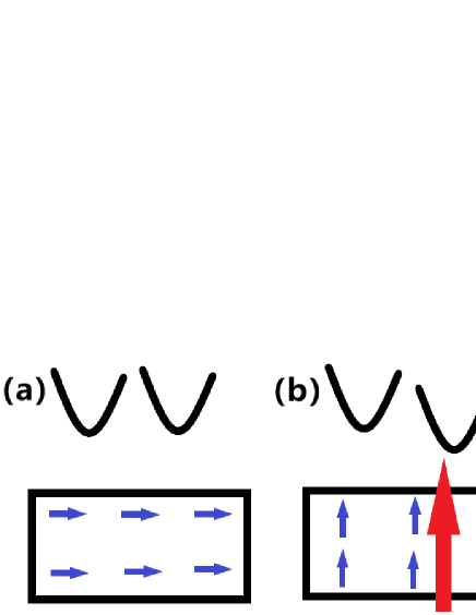
In this work, we propose a way to achieve MA transformation from in-plane to out-of-plane by electric field, and then realize valley polarization (see Figure 1). In Figure 1 (a), if a 2D material is with in-plane magnetization, no valley polarization can be observed. In Figure 1 (b), when an electric field is imposed along out-of-plane direction, the magnetization changes from in-plane to out-of-plane, and a valley polarization can be induced. Recently, 2D family with a septuple-atomic-layer structure has been established, and and of them have been synthesized by the chemical vapor deposition methoda11 ; a12 . Here, by the first-principle calculations, we use a concrete example of monolayer to illustrate our idea. Calculated results show that increasing electric filed indeed can make MA change from in-plane to out-of-plane direction in . The semiconductor properties and out-of-plane magnetization can coexist in a certain electric field region, implying that becomes a true FV material. Our findings can be extended to other 2D materials, and tune MA by electric field.
II Computational detail
Based on density-functional theory (DFT)1 , we perform the spin-polarized first-principles calculations by employing the projected augmented wave method, as implemented in Vienna ab initio simulation package (VASP)pv1 ; pv2 ; pv3 . The generalized gradient approximation of Perdew-Burke-Ernzerhof (PBE-GGA)pbe is adopted as exchange-correlation functional. To consider on-site Coulomb correlation of V atoms, the GGA+ method in terms of the on-site Coulomb interaction of 3.0 eVq14 is used within the rotationally invariant approach proposed by Dudarev et alu , where only the effective () based on the difference between the on-site Coulomb interaction parameter and exchange parameters is meaningful. The energy cut-off of 500 eV, total energy convergence criterion of eV and force convergence criteria of less than 0.0001 on each atom are adopted to attain accurate results. To avoid the interactions between the neighboring slabs, a vacuum space of more than 32 is used. The -centered 16 161 k-point meshs in the Brillouin zone (BZ) are used for structure optimization and electronic structures calculations, and 9161 Monkhorst-Pack k-point meshs for calculating FM/antiferromagnetic (AFM) energy with rectangle supercell. The SOC effect is explicitly included to investigate MCA and electronic properties of monolayer. We calculate the Berry curvatures directly from wave functions based on Fukui’s methodbm by using VASPBERRY codebm1 ; bm2 .

III Structure and magnetic anisotropy
The top and side views of crystal structure of monolayer are shown in FIG.1 of electronic supplementary information (ESI), along with the first BZ with high-symmetry points. The V, Si and P atoms are packed in a honeycomb lattice with a space group of (No.187), which has broken inversion symmetry, allowing spontaneous valley polarization. This crystal is composed of covalently bonded atomic layers in the order of P-Si-P-V-P-Si-P along the axis. In other words, the monolayer can be viewed as a -like layer sandwiched in-between two slightly buckled honeycomb SiP layers. The optimized lattice constants of (3.486 ) is good agreement with a previous reportq14 .
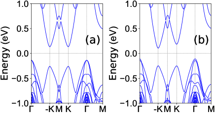
Because the magnetization is a pseudovector, the out-of-plane FM breaks all possible vertical mirror symmetry, but preserves the horizontal mirror symmetry, which allows the spontaneous valley polarization and a nonvanishing Chern number of 2D system. The is predicted to be an out-of-plane ferromagnet (a FV material) with only considering MCA energyq14 ; gsd . However, the will become a 2D- magnet (a non-FV material), when including MSA energygsd . The energy band structures with both in-plane and out-of-plane magnetization are plotted in Figure 2. It is clearly seen that is a FV material with out-of-plane magnetization, and it will become a common magnetic semiconductor with in-plane case. Thus, just flipping the magnetic anisotropy through the external field, will become a FV material. Next, we will flip the magnetic anisotropy from in-plane to out-of-plane through electric field.
Firstly, the magnetic ground state under the electric field is confirmed, and the energy differences (per formula unit) between AFM and FM ordering as a function of electric field are plotted in FIG.2 of ESI. It is found that the FM state is always ground state within considered range, and increasing can reduce the FM interaction.
The orientation of magnetization can affect magnetic, electronic and topological properties of 2D materialsq14-0 ; a4 ; a6 ; a7 . The orientation of magnetization can be determined by MAE, which mainly includes two parts: (1) MCA energy caused by the SOC; (2) MSA energy () due to the anisotropic dipole-dipole (D-D) interactiona1-7 ; a7-1 :
| (1) |
in which the and represent the local magnetic moments and vectors that connect the sites and . For monolayer with a collinear FM ordering, the () can be expressed as:
| (2) |
where and mean that spins lie in the plane and out-of-plane, and is the angle between the and . The depends on the crystal structure and local magnetic moment. To minimize magnetostatic energy, the MSA tends to make spins directed parallel to the monolayer. Usually, the MSA energy can be ignored, but MSA becomes significant to MAE for materials with weak SOC.
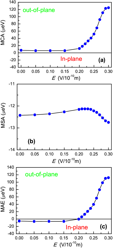
Without inclusion of SOC, there is no link between the crystalline structure and the direction of the magnetic moments. Thus, the MCA energy is calculated by from GGA++SOC calculations. The calculation includes two steps: (i) a collinear self-consistent field calculation without SOC to obtain the convergent charge density; (ii) a noncollinear non-self-consistent calculation of two different magnetization directions (The magnetization directions are in the plane () and along the axis ()) within SOC. The negative/positive MAE corresponds to an easy axis along the in-plane/out-of-plane direction. We show as a function of in Figure 3 (a). Calculated results show that the is positive within considered range. When 0.2 , the basically remains unchanged with about 6 . For 0.2 , the has a rapid increase, and reaches to 125 at 0.3 . This implies that electric filed can effectively tune . The is calculated by Equation 2. The local magnetic moment of V atom () as a function of is plotted in FIG.3 of ESI. It is found that has small change within considered range (1.08 -1.11 ). The versus is plotted in Figure 3 (b), and the changes from -12.13 to -12.75 . The MAE is calculated by =+, as shown in Figure 3 (c). When is less than 0.2 , the in-plane anisotropy can be observed due to negative MAE. When 0.2 , the positive MAE means a preferred out-of-plane magnetization. The MAE changes from negative value to positive value, implying a transition of MA from in-plane to out-of-plane induced by electric field.
IV electronic structures
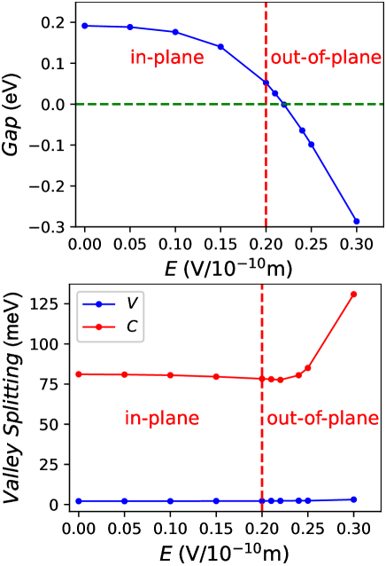
Electric field can result in semiconductor to metal transition in bilayer and apl . Thus, the electronic structures of under electric field are investigated to confirm its semiconductor properties. With fixed out-of-plane magnetization, the evolutions of total energy band gap and the valley splitting for both valence and condition bands as a function of are plotted in Figure 4. At representative , the energy band structures are plotted in Figure 5. It is found that the gap decreases with increasing , and a semiconductor to metal transition is produced at 0.22 . Combined with the previous out-of-plane MA region (0.20 ), the is intrinsically a FV material for between 0.20 and 0.22 .
Within considered range, the valley splitting of conduction band is observable, while the valley splitting of valence band can be ignored. This can be explained by distribution of V- orbitals. The V- orbitals split into orbital, + and + orbitals in a trigonal prismatic crystal field environment. According to FIG.4 of ESI, the + orbitals dominate K and -K valleys of conduction bands, while the orbitals mainly contribute to K and -K valleys of valence bands. Since the FM ordering breaks spin degeneracy between the spin-up and spin-down bands, the SOC Hamiltonian only involving the interaction of the same spin states mainly produces valley polarization. If + orbitals dominate the K and -K valleys, the valley splitting can be expressed asv2 ; v3 :
| (3) |
If the -K and K valleys are mainly from orbitals, the valley splitting is given:
| (4) |
where and / are the SOC-related constant and the resulting energy level at K/-K valley. For +-dominated -K and K valley with general magnetization orientation, v3 , where =0/90∘ for out-of-plane/in-plane magnetization. Thus, the valley splitting of for both valence and conduction bands will become zero, when is with in-pane case.
FIG.5 and FIG.6 of ESI present the calculated energy band structures and Berry curvatures of under 0.21 with SOC for magnetic moment of V along the and directions. FIG.5 (a) shows the valley polarization, and the energy of K valley is higher than one of -K valley. The valley polarization can be switched by reversing the magnetization direction from to direction (see FIG.5 (b) of ESI). The under 0.21 is an indirect band gap semiconductor with gap value of 26.4 meV. For the two situations, the opposite signs of Berry curvature around -K and K valleys can be observed. It is found that there are the unequal magnitudes of Berry curvatures at -K and K valleys. By reversing the magnetization, the magnitudes of Berry curvature at -K and K valleys exchange to each other, but their signs remain unchanged.
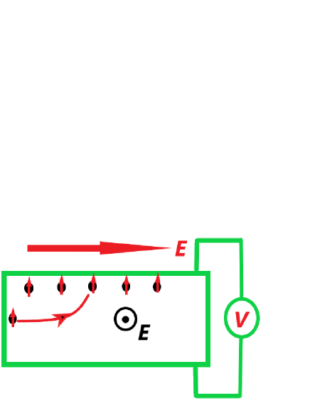
Under an in-plane longitudinal , anomalous velocity of Bloch electrons at K and -K valleys is related with Berry curvature :qqq . An appropriate electron doping makes the Fermi level fall between the -K and K valleys of conduction band. When in-plane and out-of-plane electric fields are applied, the Berry curvature forces the electron carriers to accumulate on one side of the sample, giving rise to an AVHE in monolayer (see Figure 6). In fact, for example, when out-of-plane electric field 0.24 , only -K valley of conduction band is conductive (see Figure 5), and AVHE can be achieved with applied electric fields.
V Conclusion
In summary, we have demonstrated that the electric field can result in a MA transformation
in . The electric field can induce sudden change of positive MCA energy, and has small effects on negative MSA energy.
This leads to sign change of MAE, giving rise to in-plane to out-of-plane transformation of MA. It is found that electric field can induce semiconductor-metal phase transition in . However, for a certain electric field region, semiconductor properties and out-of-plane magnetization can coexist, confirming FV properties of . When in-plane and out-of-plane electric fields are applied, an
AVHE in monolayer can be achieved.
Our findings can inspire more works of electric filed-tuned MA.
SUPPLEMENTARY MATERIAL
See the supplementary material for crystal structures; energy difference between AFM and FM and local magnetic moment of V atom as a function of ; the related energy band structures and Berry curvatures.
Conflicts of interest
There are no conflicts to declare.
Acknowledgements.
This work is supported by Natural Science Basis Research Plan in Shaanxi Province of China (2021JM-456). We are grateful to Shanxi Supercomputing Center of China, and the calculations were performed on TianHe-2.References
- (1) L. J. Sham, S. J. Allen, A. Kamgar, and D. C. Tsui, Phys. Rev. Lett. 40, 472 (1978).
- (2) S. A. Wolf, D. D. Awschalom, R. A. Buhrman, J. M. Daughton, S. von Moln r, M. L. Roukes, A. Y. Chtchelkanova, and D. M. Treger, Science 294, 1488 (2001).
- (3) H. Zeng, J. Dai, W. Yao, D. Xiao, and X. Cui, Nat. Nanotechnol. 7, 490 (2012).
- (4) K. F. Mak, K. He, J. Shan, and T. F. Heinz, Nat. Nanotechnol. 7, 494 (2012).
- (5) A. Srivastava, M. Sidler, A. V. Allain, D. S. Lembke, A. Kis, and A. Imamo glu, Nat. Phys. 11, 141 (2015).
- (6) 8 H. Zeng, J. Dai, W. Yao, D. Xiao and X. Cui, Nat. Nanotechnol. 7, 490 (2012).
- (7) D. MacNeill, C. Heikes, K. F. Mak, Z. Anderson, A. Kormnyos, V. Zlyomi, J. Park and D. C. Ralph, Phys. Rev. Lett. 114, 037401 (2015).
- (8) C. Zhao, T. Norden, P. Zhang, P. Zhao, Y. Cheng, F. Sun, J. P. Parry, P. Taheri, J. Wang, Y. Yang, T. Scrace, K. Kang, S. Yang, G. Miao, R. Sabirianov, G. Kioseoglou, W. Huang, A. Petrou and H. Zeng, Nat. Nanotechnol. 12, 757 (2017).
- (9) M. Zeng, Y. Xiao, J. Liu, K. Yang and L. Fu, Chem. Rev. 118, 6236 (2018).
- (10) W. Y. Tong, S. J. Gong, X. Wan, and C. G. Duan, Nat. Commun. 7, 13612 (2016).
- (11) Y. B. Liu, T. Zhang, K. Y. Dou, W. H. Du, R. Peng, Y. Dai, B. B. Huang, and Y. D. Ma, J. Phys. Chem. Lett. 12, 8341 (2021).
- (12) Z. Song, X. Sun, J. Zheng, F. Pan, Y. Hou, M.-H. Yung, J. Yang, and J. Lu, Nanoscale 10, 13986 (2018).
- (13) J. Zhou, Y. P. Feng, and L. Shen, Phys. Rev. B 102, 180407(R) (2020).
- (14) P. Zhao, Y. Ma, C. Lei, H. Wang, B. Huang, and Y. Dai, Appl. Phys. Lett. 115, 261605 (2019).
- (15) X. Y. Feng, X. L. Xu, Z. L. He, R. Peng, Y. Dai, B. B. Huang and Y. D. Ma, Phys. Rev. B 104, 075421 (2021).
- (16) S. Li, Q. Q. Wang, C. M. Zhang, P. Guo and S. A. Yang, Phys. Rev. B 104, 085149 (2021).
- (17) H. X. Cheng, J. Zhou, W. Ji, Y. N. Zhang and Y. P. Feng, Phys. Rev. B 103, 125121 (2021).
- (18) K. Sheng, Q. Chen, H. K. Yuan and Z. Y. Wang, Phys. Rev. B 105, 075304 (2022)).
- (19) P. Jiang, L. L. Kang, Y. L. Li, X. H. Zheng, Z. Zeng and S. Sanvito, Phys. Rev. B 104, 035430 (2021).
- (20) Y. Zang, Y. Ma, R. Peng, H. Wang, B. Huang, and Y. Dai, Nano Res. 14, 834 (2021).
- (21) R. Peng, Y. Ma, X. Xu, Z. He, B. Huang, and Y. Dai, Phys. Rev. B 102, 035412 (2020).
- (22) W. Du, Y. Ma, R. Peng, H. Wang, B. Huang, and Y. Dai, J. Mater. Chem. C 8, 13220 (2020).
- (23) R. Li, J. W. Jiang, W. B. Mi and H. L. Bai, Nanoscale 13, 14807 (2021).
- (24) S. D. Guo, J. X. Zhu, W. Q. Mu and B. G. Liu, Phys. Rev. B 104, 224428 (2021).
- (25) S. D. Guo, Y. L. Tao, K. Cheng, B. Wang and Y.-S. Ang, arXiv:2207.13420 (2022).
- (26) Z. Wang, M. Gibertini, D. Dumcenco, T. Taniguchi, K. Watanabe, E. Giannini, and A. F. Morpurgo, Nat. Nanotechnol. 14, 1116 (2019).
- (27) D. R. Klein, D. MacNeill, Q. Song, D. T. Larson, S. Fang, M. Xu, R. A. Ribeiro, P. C. Canfield, E. Kaxiras, R. Comin, and J. H. Pablo, Nat. Phys. 15, 1255 (2019).
- (28) X. B. Lu, R. X. Fei, L. H. Zhu and L. Yang, Nat. Commun. 11, 4724 (2020).
- (29) Y. L. Hong, Z. B. Liu, L. Wang T. Y. Zhou, W. Ma, C. Xu, S. Feng, L. Chen, M. L. Chen, D. M. Sun, X. Q. Chen, H. M. Cheng and W. C. Ren, Science 369, 670 (2020).
- (30) L. Wang, Y. Shi, M. Liu, A. Zhang, Y.-L. Hong, R. Li, Q. Gao, M. Chen, W. Ren, H.-M. Cheng, Y. Li, and X.- Q. Chen, Nature Communications 12, 2361 (2021).
- (31) P. Hohenberg and W. Kohn, Phys. Rev. 136, B864 (1964); W. Kohn and L. J. Sham, Phys. Rev. 140, A1133 (1965).
- (32) G. Kresse, J. Non-Cryst. Solids 193, 222 (1995).
- (33) G. Kresse and J. Furthmller, Comput. Mater. Sci. 6, 15 (1996).
- (34) G. Kresse and D. Joubert, Phys. Rev. B 59, 1758 (1999).
- (35) J. P. Perdew, K. Burke and M. Ernzerhof, Phys. Rev. Lett. 77, 3865 (1996).
- (36) S. L. Dudarev, G. A. Botton, S. Y. Savrasov, C. J. Humphreys and A. P. Sutton, Phys. Rev. B 57, 1505 (1998).
- (37) T. Fukui, Y. Hatsugai and H. Suzuki, J. Phys. Soc. Japan. 74, 1674 (2005).
- (38) H. J. Kim, https://github.com/Infant83/VASPBERRY, (2018).
- (39) H. J. Kim, C. Li, J. Feng, J.-H. Cho, and Z. Zhang, Phys. Rev. B 93, 041404(R) (2016).
- (40) X. Liu, H. C. Hsu, and C. X. Liu, Phys. Rev. Lett. 111, 086802 (2013).
- (41) S. D. Guo, J. X. Zhu, M. Y. Yin and B. G. Liu, Phys. Rev. B 105, 104416 (2022).
- (42) S. D. Guo, W. Q. Mu and B. G. Liu, 2D Mater. 9, 035011 (2022).
- (43) K. Yang, G. Y. Wang, L. Liu , D. Lu and H. Wu, Phys. Rev. B 104, 144416 (2021).
- (44) Q. Y. Wu, L. M. Cao, Y. S. Ang and L. K. Ang, Appl. Phys. Lett. 118, 113102 (2021).
- (45) P. Zhao, Y. Dai, H. Wang, B. B. Huang and Y. D. Ma, ChemPhysMater, 1, 56 (2022).
- (46) R. Li, J. W. Jiang, W. B. Mi and H. L. Bai, Nanoscale 13, 14807 (2021).
- (47) D. Xiao, M. C. Chang, and Q. Niu, Rev. Mod. Phys. 82, 1959 (2010).