Enhancing the Coherence of Superconducting Quantum Bits with Electric Fields
Abstract
In the endeavour to make quantum computers a reality, integrated superconducting circuits have become a promising architecture. A major challenge of this approach is decoherence originating from spurious atomic tunneling defects at the interfaces of qubit electrodes, which may resonantly absorb energy from the qubit’s oscillating electric field and reduce the qubit’s energy relaxation time . Here, we show that qubit coherence can be improved by tuning dominating defects away from the qubit resonance using an applied DC-electric field. We demonstrate a method that optimizes the applied field bias and enhances the 30-minute averaged qubit time by 23%. We also discuss how local gate electrodes can be implemented in superconducting quantum processors to enable simultaneous in-situ coherence optimization of individual qubits.
Introduction
Superconducting integrated circuits have evolved into a powerful architecture for creating artificial quantum systems. In state-of-the-art experiments, tens of qubits are coherently operated as quantum simulators and universal processors[1, 2, 3, 4] while access to prototype devices is being offered via the cloud to accelerate the development of practical quantum algorithms[5]. On the way forward, mitigating decoherence is one of the central challenges, because it hinders further up-scaling and implementation of quantum error correction[6, 7].
Today’s processors typically employ transmon qubits that are based on discrete energy levels in non-linear LC-resonators formed by a capacitively shunted Josephson junction[8].
A large part of decoherence in such qubits is due to dielectric loss in the native surface oxides of the capacitor electrodes[9, 10]. This loss shows a remarkably structured frequency dependence [11, 12] which originates in the individual resonances of spurious atomic tunneling defects[13].
These defects form a sparse bath of parasitic two-level quantum systems, so-called TLS, which have been evoked long ago to explain the anomalous low-temperature properties of amorphous materials [14, 15].When a TLS has an electric dipole moment, it may resonantly absorb energy from the oscillating electric field of the qubit mode, and efficiently dissipate it into the phonon- [16] or BCS quasiparticle bath [17].
Moreover, TLS resonance frequencies may fluctuate in time due to interactions with thermally activated, randomly switching low-energy TLS[18, 19, 20, 21, 22].
This mechanism efficiently transforms thermal noise into the qubit’s environmental spectrum, and causes fluctuations of the qubit’s resonance frequency and energy relaxation rate [23, 24, 25]. For quantum processors, this implies fluctuations of their quantum volume (i.e. computational power)[26].
Recently, we have shown that the resonance frequencies of TLS located on thin-film electrodes and the substrate of a qubit circuit can be tuned by an applied DC-electric field [10, 27]. Accordingly, it becomes possible to tune defects that dominate qubit energy relaxation away from the qubit resonance, and this results in longer relaxation times .
Here, we demonstrate this concept using a simple routine which maximizes the time of a qubit by searching for an optimal electric field bias. The method was tested at various qubit resonance frequencies and increased the 30-minute averaged qubit time by 23%.
Electric field tuning of TLS
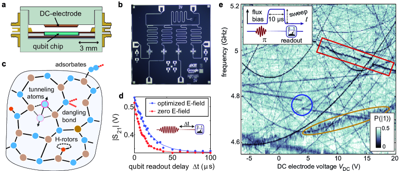
For our experiments, we fabricated a transmon qubit sample in the so-called ’X-Mon’ design following Barends et al. [12] as shown in Fig. 1 b. The flux-tunable qubit uses a submicron-sized Al/AlOx/Al tunnel junction made by shadow evaporation as described in detail in Ref. [28].
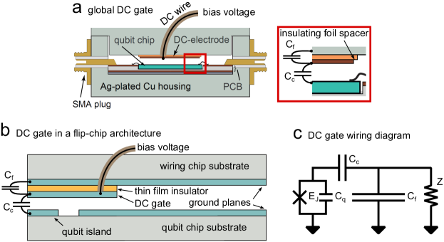
The electric field for TLS tuning is generated by a DC-electrode installed on the lid of the sample housing above the qubit chip’s surface as illustrated in Fig. 1a. The electrode is made from a copper foil that is insulated by Kapton foil from the housing. To improve E-field homogeneity in vicinity of the qubits, the electrode has a comparable size than the qubit chip. More details on this setup are described in Ref. [10].
The response of TLS to the applied electric field is observed by measuring the qubit energy relaxation time as a function of qubit frequency, which shows Lorentzian minima whenever sufficiently strongly interacting TLS are tuned into resonance. A detailed view on the rich TLS spectrum as shown in Fig. 1 e is obtained using swap-spectroscopy [29]. With this protocol, TLS are detected by the resonant reduction of the qubit’s excited state population after it was tuned for a fixed time interval to various probing frequencies. In the studied sample, only a single TLS was observed that did not couple to the applied E-field, indicating that it was likely residing in a tunnel barrier of the submicron-sized qubit junctions where no DC-electric field exists [8]. This confirms that only a few resonant TLS are typically found in small area Josephson junctions[30, 6, 28], and dielectric loss is dominated by defects on the interfaces of the qubit electrodes[10, 27, 9]. This is true as long as qubits are fabricated with methods [31, 32, 33] that avoid the formation of large-area stray Josephson junctions which are known to contribute many additional defects [10, 28].
In Fig. 1 e, some TLS are observed whose resonance frequencies show strong fluctuations or telegraphic switching due to their interaction with low-energy TLS that are thermally activated.
We note that TLS may also interact with classical bistable charge fluctuators that have a very small switching rate between their states. Since these fluctuators may also be tuned by the applied electric field, hysteresis effects may appear in electric field sweeps since the state of a fluctuator, and hereby the resonance frequency of a high-energy TLS, may depend on the history of applied E-fields [34]. An example of such an interacting TLS-fluctuator system is marked by the blue circle in Fig. 1 e, where the resonance frequency of a TLS abruptly changed.
Method for optimizing the qubit time
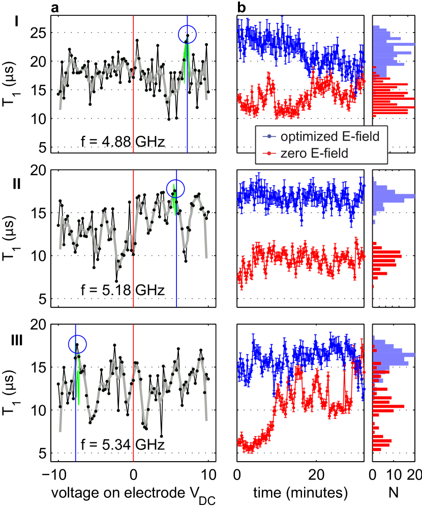
As it is evident from Fig. 1 e, at each qubit operation frequency there is a preferable electric field bias where most of the dominating TLS are tuned out of qubit resonance and the time is maximized.
In the following, we describe a simple routine by which an optimal E-field bias can be automatically determined.
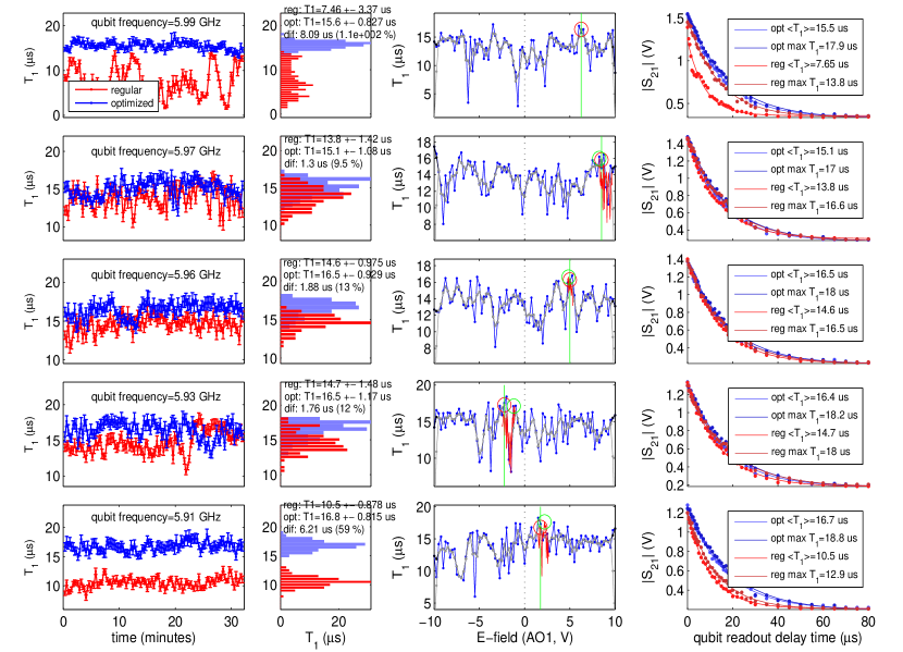
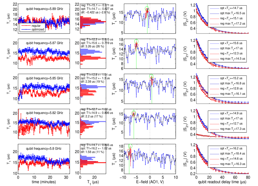
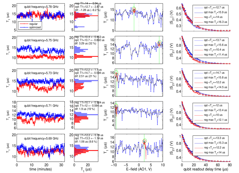
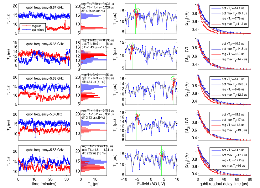
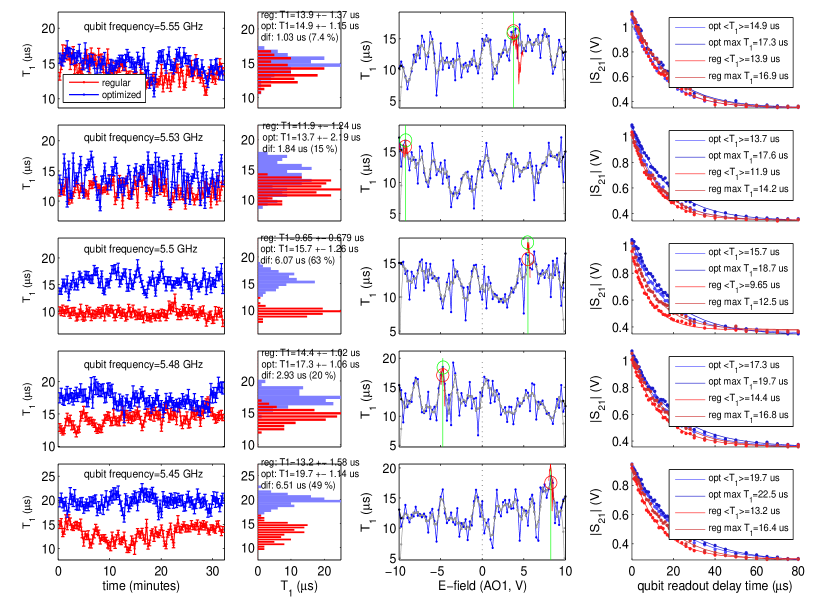
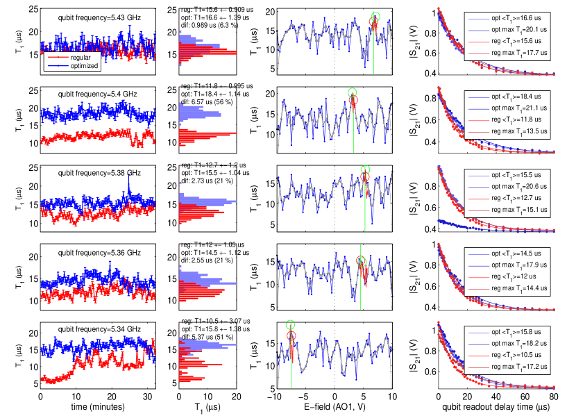
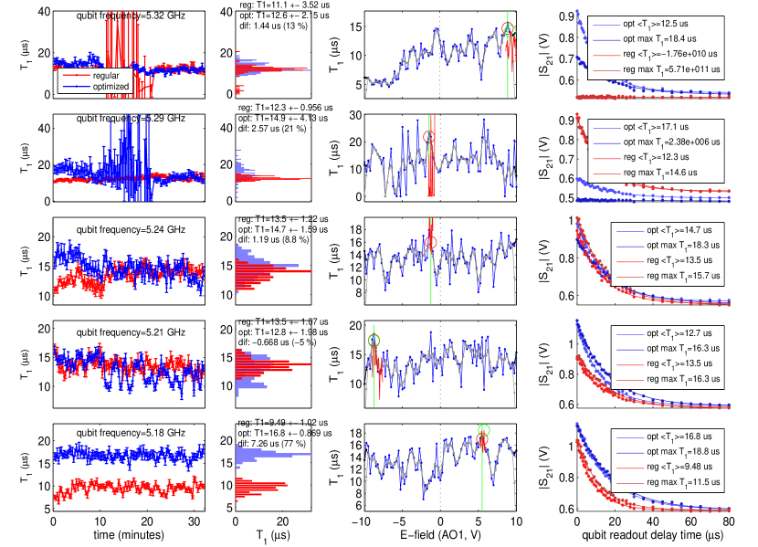
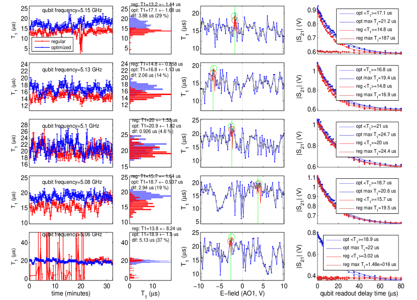
First, the qubit -time is measured for a range of applied electric fields. Hereby, the -time is obtained from exponential fits to the decaying qubit population probability after it was excited by a microwave pulse, measured using the common protocol shown in the inset of Fig. 1 d.
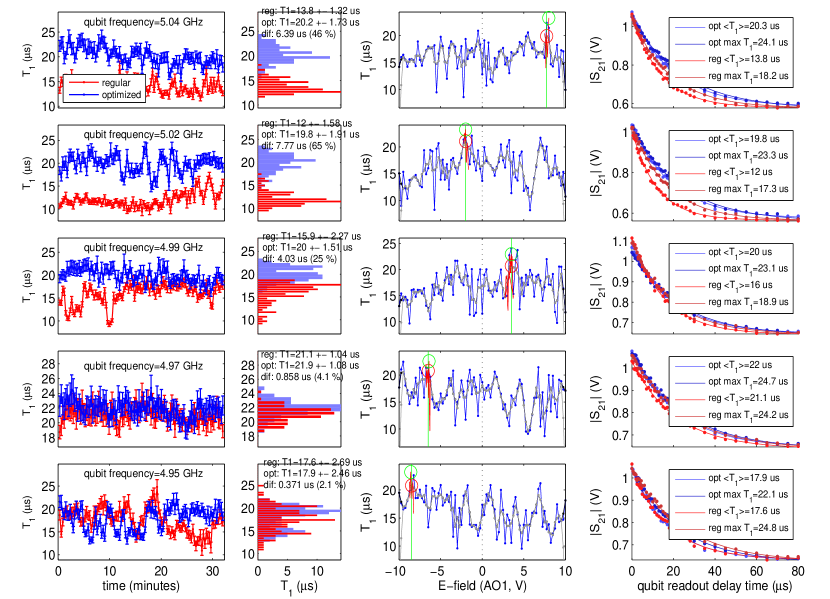
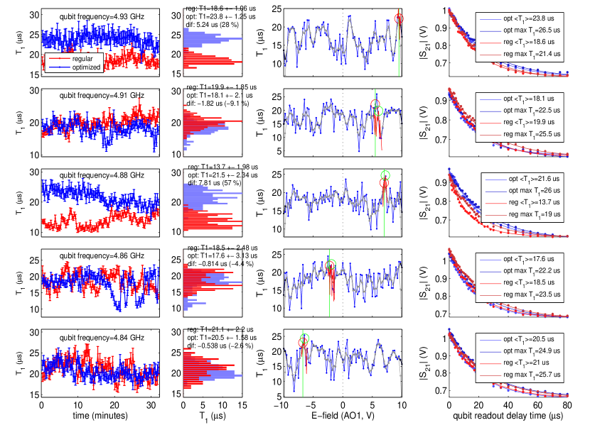
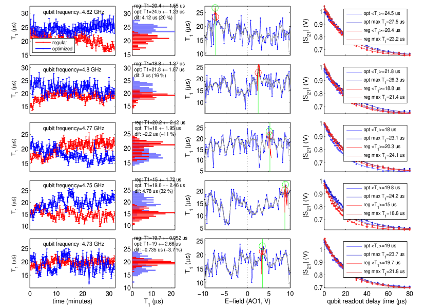
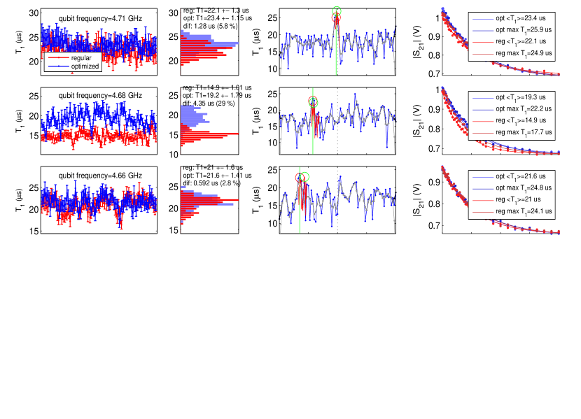
Figure 2a shows the resulting electric field dependence of (black data points), measured at various qubit resonance frequencies (rows I to III).
These data are then smoothed by a nearest-neighbour average (gray curve) to average out individual dips and peaks in order to amplify broader maxima that promise a more stable improvement.
Next, the E-field is set to the value where the maximum -time occurred (blue circle in Fig. 2 a). Hereby, it is recommended to approach the detected optimal E-field from the same value where the previous E-field sweep was started. This helps to avoid the mentioned possible hysteresis effects in the TLS resonance frequencies that may occur when they are coupled to meta-stable field-tunable TLS whose state depends on the history of applied E-fields.
Finally, a second pass is performed, sweeping the E-field in finer steps around its previously determined optimum value until the obtained time is close to the maximum value that was observed in the previous sweep. This ensures that hysteresis effects are better compensated and the finer step helps to avoid sharp dips that were not resolved in the first pass. Data obtained in the second pass are plotted in green in Fig. 2 a).
Benchmarking the method
To test the efficiency of the optimization routine, first the qubit is repeatedly observed during 30 minutes at zero applied electric field as a reference (red data in Fig. 2 b). Afterwards, the optimization routine searches for the electric field which maximizes the qubit’s coherence time by taking data as shown in Fig. 2 a. The result is then checked by monitoring the -time at the found optimal E-field during another 30 minutes (blue data in Fig. 2 b).
Evidently, during most of this time, acquired times after optimization are higher than the reference values that were obtained at zero applied electric field.
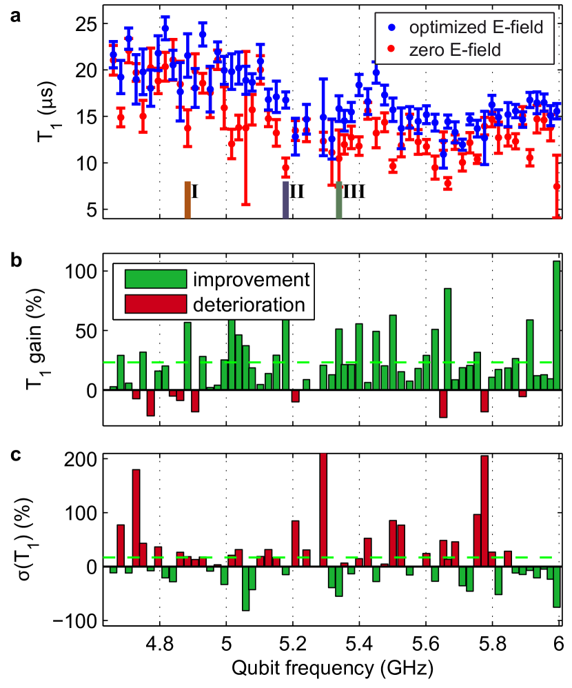
To measure the average improvement of the optimization routine, the benchmarking protocol was repeated at various (in total 59) qubit resonance frequencies, see the supplementary material for the full data set.
Figures 3a and b summarize the absolute and relative improvement of the qubit -time at all investigated qubit resonance frequencies. In most cases (), the routine improved the 30-minute average qubit -time. The improvement was larger than 10% in 67% of cases, and enhanced by more than 20% in 46% of all tries.
The few cases where the averaged -time was smaller after optimization were caused by TLS resonance frequency fluctuations occurring during the 30-minute averaging interval. In quantum processors, such deterioration can be detected on the basis of qubit error rates and trigger a renewed E-field optimization.
Averaged over all tested qubit resonance frequencies and a 30-minute time interval past optimization, the time improvement was . We expect that similar improvements are possible also in state-of-the-art transmon qubits, as all of them show time-dependent and sample specific time variations which indicate their limitation by randomly occuring TLS [24, 13, 19, 20, 21].
As a consequence of the defects’ resonance frequency fluctuations, the enhancement (gain) of the time tends to diminish with time that has passed after the E-field optimization. A further analysis (see supplementary material I and II) indicates that the average gain drops from an initial value of about 30% immediately after optimization to slightly above 20% after 30 minutes past optimization.
To check how much the optimization routine affects the temporal fluctuation strength of the qubit’s time, the standard deviation of observed times during the 30 minute intervals before and after optimization were compared. The result is shown in Figure 3c. In slightly more than half cases (59%), the time fluctuations increased after optimization. This might be mitigated by enhancing the optimization algorithm such that it prefers broader -time peaks which are less sensitive to TLS frequency fluctuations, and by including the fluctuation strength at detected peaks as a criterion.
Proposed integration with quantum processors
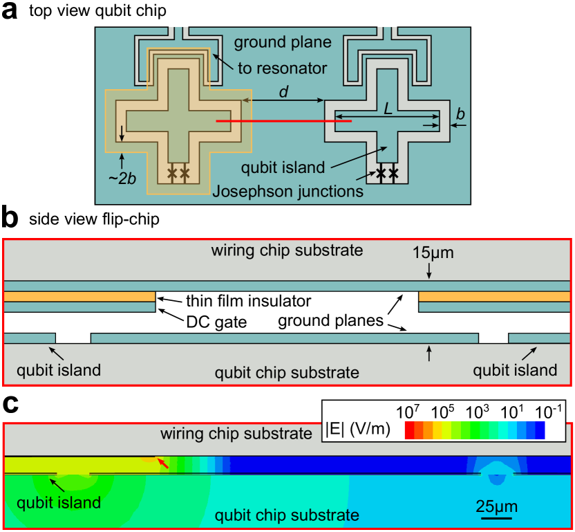
When each qubit in a processor is coupled to a dedicated local gate electrode, the optimization routine can be applied simultaneously on all qubits. This tuneup-process is facilitated when no cross-talk of a gate electrode to neighboring qubits occurs. Moreover, the generated electric field should be sufficiently strong all along the edges of the qubit island and the opposing ground plane (where surface defects are most strongly coupled to the qubit [10]), so that all relevant TLS can be tuned by MHz to decouple them from the qubit. Assuming a relatively small coupling TLS dipole moment component of Å [10, 35, 11], this corresponds to required field strengths kV/m. Given a typical distance between the DC-electrode and the qubit electrodes of below 1 mm, such E-fields are unproblematically obtained with a bias voltage of a few Volt on the DC-electrode.
Figure 4 shows a possible implementation of a gate electrode array, which is located on a separate wiring chip that is bumb-bonded to the chip carrying the qubits in a flip-chip configuration [36, 37]. In Fig. 4 a, a top view of two Xmon-type [12] qubits is shown, where the gate electrode above the left qubit is indicated in orange. The electrode extends slightly over the edges of the qubit island’s opposing ground plane to ensure the tunability of TLS in this region.
The cross section of the chip stack is sketched in Fig. 4 b, showing that the gate electrodes are separated from the ground plane of the wiring chip by a thin film insulator.
The simulated electric field strength in this region is drawn to-scale in Fig. 4 c, for the case when the left electrode is biased at while all other metallic parts (including the qubit island [10]) are kept at zero potential.
As expected, the induced field strength decays on a length scale of roughly the distance between the two chips, given that qubits are surrounded by a ground plane and also the wiring chip has a ground plane. For a qubit-to-qubit separation of as used in the presented simulation, we accordingly find the cross-talk to be below .
Alternatively, the local electrodes could also be placed on the backside of the qubit chip. In this case, the substrate thickness will determine the horizontal field screening length, and stronger cross-talk can be expected. However, FEM simulations of the induced E-fields in a given processor layout should allow one to sufficiently compensate for this cross-talk.
The capacitive coupling of the qubit to the gate electrode introduces extra decoherence channels: dielectric loss occurs in the insulation separating the electrode from ground, and by radiative loss, the qubit dissipates energy into the electrode wiring. These losses depend strongly on the dimensions of the electrode. We find (see supplementary material) a qubit limitation of 5 ms for the setup used in this work, and estimate similar values for the proposed integration into flip-chip quantum processors.
Conclusion
We present an experimental setup and an automatic routine that extends the energy relaxation time of superconducting transmon qubits. The idea is to expose the qubit electrodes to a DC-electric field at which the most detrimental TLS-defects are tuned out of qubit resonance. Averaging over qubit working frequencies and a 30-minute time interval (that was limited by time constraints), the -time was improved by 23% compared to zero applied electric field.
In our experiments, the optimization routine took less than 10 minutes (to acquire about 60 values of qubit at several E-fields). However, the data shown in Fig. 2 a suggests that the range of applied E-fields may be reduced, which together with further optimizations such as less averaging in individual -time measurements, may reduce the optimization time to about one minute.
Analysis of the raw data such as shown in Fig. 2 and in the supplementary material suggests that more stable improvements might be achieved by improving the algorithm, e.g. by including the width of a peak in vs. E-field as a criterion next to the height of the peak.
Moreover, we expect that deterioration of the 30-minute average qubit time by the optimization routine, as it occurred in a few () cases in these tests, can be avoided by averaging over several E-field sweeps to better account for TLS showing strong resonance frequency fluctuations. Also, one may devise a linear or machine-learning feedback mechanism that regularly readjusts the E-field bias on the basis of the steady stream of qubit error rates obtained during quantum algorithms to ensure continuous coherence enhancement.
The ability to tune TLS out of resonance with a qubit is especially beneficial for processors implementing fixed-frequency qubits, which can be tuned only in a limited range by exploiting the AC-stark shift[CarrollACstark]. This may still allow one to improve qubit coherence by evading strongly coupled TLS as it was recently demonstrated by Zhao et al.[38]. However, even when tunable qubits are used, it is still necessary to mutually balance their individual resonance frequencies to avoid crosstalk and to maximize gate fidelities, and this will be greatly simplified if qubit coherence can be optimized at all frequencies by having independent control of the TLS bath. Also, to improve two-qubit gates that require qubit frequency excursions, one could adjust our optimization procedure to minimize the number of TLS that have resonances in the traversed frequency interval.
Our simulations indicated that it is straight-forward to equip each qubit in a processor with local gate electrodes, which will allow one to simultaneously improve of all qubits. We thus see good opportunities for this technique to become a standard in superconducting quantum processors.
Methods
Data Availability
The data that support the findings of this study are available from the corresponding author upon reasonable request.
Acknowledgements
This work was funded by Google LLC which is gratefully acknowledged. We thank for funding from the Baden-Württemberg-Stiftung (Project QuMaS), and for funding from the Bundesministerium für Forschung und Bildung in the frame of the projects QSolid and GeQCoS. We acknowledge support by the KIT-Publication Fund of the Karlsruhe Institute of Technology.
Author contribution
JL devised and implemented idea and method, performed the experiments, and analyzed the data. AB built the qubit setup for E-field tuning, designed and fabricated the investigated qubits, and performed FEM simulations. The manuscript was written by JL with assistance from AB.
Competing interests
The Authors declare no competing financial or non-financial interests.
References
- [1] Arute, F. et al. Quantum supremacy using a programmable superconducting processor. Nature 574, 505–510 (2019).
- [2] Jurcevic, P. et al. Demonstration of quantum volume 64 on a superconducting quantum computing system. Quantum Sci. Technol. 6, 025020 (2021).
- [3] Otterbach, J. et al. Unsupervised machine learning on a hybrid quantum computer. arXiv preprint arXiv:1712.05771 (2017).
- [4] Wu, Y. et al. Strong quantum computational advantage using a superconducting quantum processor. Phys. Rev. Lett. 127, 180501 (2021).
- [5] Blinov, S., Wu, B. & Monroe, C. Comparison of cloud-based ion trap and superconducting quantum computer architectures. AVS Quantum Sci. 3, 033801 (2021).
- [6] Murray, C. E. Material matters in superconducting qubits. Mater. Sci. Eng., R 146, 100646 (2021).
- [7] Kjaergaard, M. et al. Superconducting qubits: Current state of play. Annu. Rev. Condens. Matter Phys. 11, 369–395 (2020).
- [8] Koch, J. et al. Charge-insensitive qubit design derived from the cooper pair box. Phys. Rev. A 76, 042319 (2007).
- [9] Wang, C. et al. Surface participation and dielectric loss in superconducting qubits. Appl. Phys. Lett. 107, 162601 (2015).
- [10] Lisenfeld, J. et al. Electric field spectroscopy of material defects in transmon qubits. npj Quantum Inf. 5, 1–6 (2019).
- [11] Martinis, J. M. et al. Decoherence in Josephson qubits from dielectric loss. Phys. Rev. Lett. 95, 210503 (2005).
- [12] Barends, R. et al. Coherent josephson qubit suitable for scalable quantum integrated circuits. Phys. Rev. Lett. 111, 080502 (2013).
- [13] Müller, C., Cole, J. H. & Lisenfeld, J. Towards understanding two-level-systems in amorphous solids: insights from quantum circuits. Rep. Prog. Phys. 82, 124501 (2019).
- [14] Phillips, W. A. Two-level states in glasses. Rep. Prog. Phys. 50, 1657 (1987).
- [15] Anderson, P. W., Halperin, B. I. & Varma, C. M. Anomalous low-temperature thermal properties of glasses and spin glasses. Philos. Mag. 25, 1–9 (1972).
- [16] Jäckle, J. On the ultrasonic attenuation in glasses at low temperatures. Z. Phys. A: Hadrons Nucl. 257, 212–223 (1972).
- [17] Bilmes, A. et al. Electronic decoherence of two-level systems in a josephson junction. Phys. Rev. B 96, 064504 (2017).
- [18] Black, J. L. & Halperin, B. I. Spectral diffusion, phonon echoes, and saturation recovery in glasses at low temperatures. Phys. Rev. B 16, 2879 (1977).
- [19] Klimov, P. V. et al. Fluctuations of energy-relaxation times in superconducting qubits. Phys. Rev. Lett. 121, 090502 (2018).
- [20] Schlör, S. et al. Correlating decoherence in transmon qubits: Low frequency noise by single fluctuators. Phys. Rev. Lett. 123, 190502 (2019).
- [21] Burnett, J. J. et al. Decoherence benchmarking of superconducting qubits. npj Quantum Inf. 5, 54 (2019).
- [22] Carroll, M., Rosenblatt, S., Jurcevic, P., Lauer, I. & Kandala, A. Dynamics of superconducting qubit relaxation times. npj Quantum Inf. 8, 1–7 (2022).
- [23] Faoro, L. & Ioffe, L. B. Internal Loss of Superconducting Resonators Induced by Interacting Two-Level Systems. Phys. Rev. Lett. 109, 157005 (2012).
- [24] Müller, C., Lisenfeld, J., Shnirman, A. & Poletto, S. Interacting two-level defects as sources of fluctuating high-frequency noise in superconducting circuits. Phys. Rev. B 92, 035442 (2015).
- [25] Burnett, J. et al. Evidence for interacting two-level systems from the 1/f noise of a superconducting resonator. Nat. Commun. 5, 4119 (2014).
- [26] Pelofske, E., Bärtschi, A. & Eidenbenz, S. Quantum volume in practice: What users can expect from nisq devices. IEEE Trans. Quantum Eng. 3, 1–19 (2022).
- [27] Bilmes, A. et al. Resolving the positions of defects in superconducting quantum bits. Sci. Rep. 10, 1–6 (2020).
- [28] Bilmes, A., Volosheniuk, S., Ustinov, A. V. & Lisenfeld, J. Probing defect densities at the edges and inside josephson junctions of superconducting qubits. npj Quantum Inf. 8, 1–6 (2022).
- [29] Lisenfeld, J. et al. Observation of directly interacting coherent two-level systems in an amorphous material. Nat. Commun. 6, 6182 (2015).
- [30] Kim, Z. et al. Anomalous avoided level crossings in a cooper-pair box spectrum. Phys. Rev. B 78, 144506 (2008).
- [31] Dunsworth, A. et al. Characterization and reduction of capacitive loss induced by sub-micron josephson junction fabrication in superconducting qubits. Appl. Phys. Lett. 111, 022601 (2017).
- [32] Osman, A. et al. Simplified josephson-junction fabrication process for reproducibly high-performance superconducting qubits. Appl. Phys. Lett. 118, 064002 (2021).
- [33] Bilmes, A., Händel, A. K., Volosheniuk, S., Ustinov, A. V. & Lisenfeld, J. In-situ bandaged josephson junctions for superconducting quantum processors. Supercond. Sci. Technol. 34, 125011 (2021).
- [34] Meißner, S. M., Seiler, A., Lisenfeld, J., Ustinov, A. V. & Weiss, G. Probing individual tunneling fluctuators with coherently controlled tunneling systems. Phys. Rev. B 97, 180505 (2018).
- [35] Hung, C.-C. et al. Probing hundreds of individual quantum defects in polycrystalline and amorphous alumina. Phys. Rev. Appl. 17, 034025 (2022).
- [36] Foxen, B. et al. Qubit compatible superconducting interconnects. Quantum Sci. Technol. 3, 014005 (2017).
- [37] Kosen, S. et al. Building blocks of a flip-chip integrated superconducting quantum processor. Quantum Sci. Technol. (2022).
- [38] Zhao, P., Ma, T., Jin, Y. & Yu, H. Combating fluctuations in relaxation times of fixed-frequency transmon qubits with microwave-dressed states. Phys. Rev. A 105 (2022).
- [39] URL https://phys.libretexts.org/Bookshelves/Electricity_and_Magnetism/Book%3A_Electromagnetics_II_(Ellingson)/04%3A_Current_Flow_in_Imperfect_Conductors/4.02%3A_Impedance_of_a_Wire.
- [40] Sank, D. T. Fast, accurate state measurement in superconducting qubits. Phd thesis, University of California, Santa Barbara (2014).
- [41] URL https://www.dupont.com/content/dam/dupont/amer/us/en/products/ei-transformation/documents/EI-10142_Kapton-Summary-of-Properties.pdf.
Supplementary Material
S 1 Estimation of energy losses from the global DC gate
Radiative loss
We estimate the limitation of the qubit energy relaxation time by radiative loss into the wiring channel of the DC electric gate. Here, we discuss the case of a large ("global") gate electrode above the chip, as used in our experiment and illustrated in Supplementary Figure S1 a. The effective DC gate wiring diagram is shown in Supplementary Figure S1 c where is the qubit’s coupling capacitance to the DC gate, and the large filter capacitance of the DC gate to ground (), as indicated in the panel a. The qubit circuit is given by the Josephson junction (defining the qubit Josephson energy ) which is connected in parallel to the qubit total shunt capacitance (defining the qubit charging energy ). Here, is the sum of the qubit’s island capacitance to the chip’s ground plane and the Josephson junction’s self capacitance (). The copper DC wire (length , radius ) is used to control the voltage, and it has an impedance of [39], where is the specific conductivity of copper at a temperature of (we assume that the Cu conductivity does not change largely at lower temperatures), and is the qubit resonance frequency. If the gate was connected to a standard impedance-matched coaxial RF cable, would be .
The radiative loss of a transmon qubit which is capacitively coupled to an RF port has been calculated e.g. in the thesis by D. Sank [40], see Equation (D.9):
| (1) |
where is the loaded quality factor of the qubit coupled to the RF port, and is the characteristic qubit impedance. The Josephson inductance is given by , where the phase drop across the qubit Josephson junction in the Transmon qubit is . Finally, is the real part of the RF port impedance which contributes to radiative losses of the qubit into the bandwidth of the RF port. In our case, we regard our DC gate as an RF port with an effective impedance which results from the parallel connection of the wire impedance and the impedance from the filter capacitance. The radiation-limited energy relaxation time is given by:
| (2) |
where is the qubit resonance frequency.
Dielectric loss
Here, we account for dielectric losses in the filter capacitance which is indicated in Supplementary Figure S1 a and c. In our experiment we used a global gate whose dielectric is a Kapton foil (loss tangent , and [41]). The participation ratio of the filter capacitor is calculated as the qubit energy stored in divided by the total qubit energy, i.e.
| (3) | ||||
| (4) | ||||
| (5) |
where is the root mean square of the oscillating voltage across the qubit Josephson junction, or in other words the qubit’s vacuum voltage fluctuations. The small portion of that drops across the filter capacitor is . The simplified expression for results from . The added energy loss from the filter dielectric is then
| (6) |
where is the qubit energy relaxation time limitation by this dielectric loss.
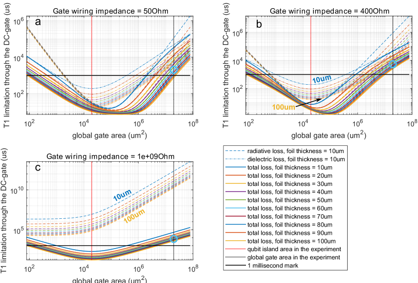
In Supplementary Figure S2 b-c, the estimated (dashed line) and (dot-dashed line) as well as the resulting total energy relaxation time limitation (continuous line) are plotted vs. the area of the global gate which is connected a via a hypothetical RF line (), or b via a DC line as described above (), or c in another hypothetical case when the gate is floating (we model the floating gate by choosing some huge number ). Note in Supplementary Figure S2 that the dielectric loss in the filter capacitor (obviously) does not depend on the wiring impedance. The gate is circular and is placed centrally above the qubit. The distance between the qubit plane and the global gate is . In the experiment the gate diameter is ,
the corresponding gate area is indicated by a black dotted line. The qubit has an Xmon topology while its island area is , where is the qubit trace width (gap of ), and its length. The legend in Supplementary Figure S2 denotes various insulating film thicknesses. The cyan circle in b emphasizes the total limitation by the DC gate of about in our experiment (insulating film thickness of ), which is dominated by dielectric loss.
Notes
The red dotted line in Supplementary Figure S2 b denotes the area of the qubit island. We see that the radiative losses are minimal if the global gate had a much smaller or a much larger footprint than the qubit island. For a small global gate, this is due to the small which maximizes in (1). For large global gate areas, the filter capacitance is practically shorting the DC wire to ground. Similarly, the dielectric losses are rather weak for a small or a large global gate when the filter capacitor’s participation ration becomes small. In Supplementary Figure S2 a a hypothetical case is presented if the global gate was connected through a -matched RF line. In such case one would expect increased radiative losses, however the total limitation would not go below . Another hypothetical scenario, which we consider to check the validitiy of our model, is presented in Supplementary Figure S2 c, where we consider the radiative loss if the global gate was floating (we model this by choosing a huge impedance for the gate wiring). As expected, we see that radiative losses then become negligible.
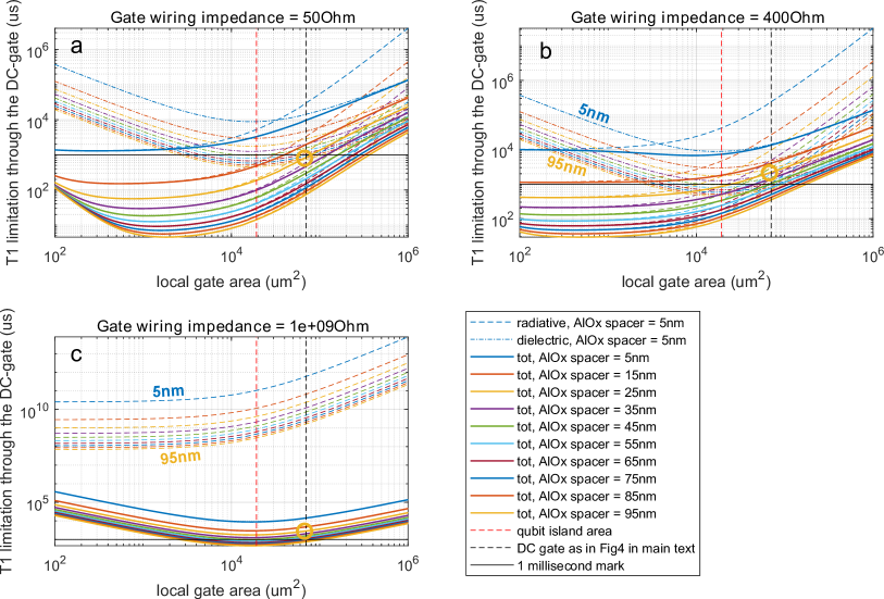
S 2 Estimation of energy loss from a local DC gate
Here, we estimate radiative dielectric loss from the individual DC-gate as proposed in the main text for integration into quantum processors (Fig. 4), and shown in Supplementary Figure S1b. The wiring diagram is shown in Fig S1c, it is identical to the setup with the global gate Supplementary Figure S1a. The only difference is that in the flip-chip architecture, the Xmon’s arm length needs to be shortened to in order to keep the qubit total shunt capacitance at . The energy relaxation time limitation due to radiative loss is given in Eq. (1), and that due to dielectric loss in the AlO spacer (assuming ) is given in Eq. (6).
The limitation is shown as a function of the local gate in Supplementary Figure S3. In a, b and c, we consider the cases of the local gate connected via a -matched RF line, a high-impedance DC line, or a 1 G impedance, respectively. The orange circle in b denotes the total limitation of about when the DC gate is controlled via a DC-wire, and the AlO has a realistic thickness of . Shown in c is the case when the local gate is assumed to be floating, which results in negligible radiative loss.
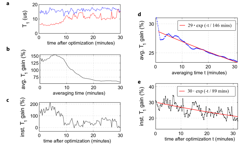
S 3 -enhancement as a function of time
As a consequence of the defect’s resonance frequency fluctuations, the enhancement (gain) of the time tends to diminish with time that has passed after the E-field optimization. Here, we characterize two types of gain: the instantaneous gain is the individual improvement measured at the corresponding time :
where is the time measured at zero electric field at the time after the beginning of the 30-minute observation interval, and is the time measured at optimized electric field at the time after the optimization was done. The average gain denotes the average over the instantaneous improvements up to a certain time since optimization.
To illustrate this, Supplementary Figure S4 shows exemplary data of times measured before and after optimization, and the corresponding average and instantaneous gains.
Figures S4d and e show average and instantaneous gains, respectively, that are averaged over all repetitions taken at 60 different qubit frequencies. Both average and instantaneous gain drop from initial values of 30% directly after optimization to slightly above 20% after 30 minutes past optimization. To get a feeling for the time scale on which the gain dwindles, we added fits to an exponential decay law: (red lines in Figs. S4d and e), which result in =29 (30) and =146 (89) minutes for average (instantaneous) gains.
S 4 Additional data
Supplementary Figures S5 - S10 show the full data set acquired from the optimization routine at various qubit resonance frequencies.