Corrections to the reflectance of graphene by light emission
Abstract
Monolayer graphene absorbs 2.3 percent of the incident visible light. This “small” absorption has been used to emphasize the visual transparency of graphene, but it in fact means that multilayer graphene absorbs a sizable fraction of incident light, which causes non-negligible fluorescence. In this paper, we formulate the light emission properties of multilayer graphene composed of tens to hundreds of layers using a transfer matrix method and confirm the method’s validity experimentally. We could quantitatively explain the measured contrasts of multilayer graphene on SiO2/Si substrates and found sizable corrections, which cannot be classified as incoherent light emissions, to the reflectance of visible light. The new component originates from coherent emission caused by absorption at each graphene layer. Multilayer graphene thus functions as a partial coherent light source of various wavelengths, and it may have surface-emitting laser applications.
I Introduction
The visual detection of graphene on Si substrates involves a complex scientific aspect related to the interference effects of light. [1, 2, 3] To enhance visibility, it is crucial for the contrast between the reflectances from the substrate and the graphene layer to be sufficiently large. Si substrates with a specific thickness of () are known to provide advantages in this context. [4, 5] Specifically, when the optical path length difference of the layer is one-half or three-half the wavelength of the incident light, the contrast reaches its maximum.
The enhanced visibility of graphene is primarily attributed to a substrate-induced enhancement of light absorption. This enhancement is valuable not only for graphene detection but also for exploring notable phenomena. For instance, the reflectance of specific graphene multilayers on SiO2/Si substrates can be reduced to zero for normally incident visible light with a wavelength () approximately equal to . Zero reflectance is achieved through destructive interference caused by and a significant absorption coefficient of graphene. [6, 7, 8] More importantly, the reflectance of multilayer graphene on SiO2/Si substrates is intricately determined because the significant absorption may result in non-negligible luminescence. This luminescence also functions as a secondary light source, leading to more sophisticated interference effects of light. [9, 10, 11, 12, 13, 14, 15]
Since graphene lacks an energy bandgap, unlike semiconductors, it is naturally expected that the impact of light emission on its optical properties is negligible. However, electrons that have absorbed light undergo various relaxation processes towards the ground state, [16, 17] generally involving luminescence contributions. For instance, Lui et al. [12] and Suemoto et al. [14] have reported that graphene and graphite emit light under femtosecond laser pulse excitation, respectively. In this paper, we demonstrate that, despite the tiny branching ratio of light emission to absorption, light emission constitutes the primary correction to visible reflectance, thanks to the substantial absorption of graphene. We have found this notable feature for the first time by leveraging both the destructive interference effects of substrates and the coherence of the multilayer structure. Additionally, we can show that light emission significantly contributes to enhancing the visibility of graphene on a substrate.
In this study, we delineate coherent and incoherent corrections to the reflectance of multilayer graphene (on SiO2/Si substrates) caused by the light it emits after absorbing incident light. The coherent corrections are dependent on only two parameters: the branching ratio () of coherent light emission to absorbed light and the phase ( or ) of the emitted light. Both parameters are assumed to be independent of the number of layers () and the wavelength of light. Contrasts (reflectivities) calculated using these phenomenologically determined parameters show reasonable agreement with measured values for various . Despite the branching ratio, determining the strength of light emitted from a graphene monolayer, being less than one percent, the coherent components become the primary corrections to the reflectance of multilayer graphene. This is due to the coherence increasing the amplitude of reflection through constructive interference. Furthermore, based on the observation that the phase of reflection and transmission coefficients of each layer translates into the amplitude of the emitted light, we hypothesize that the origin of the coherent components is coherent light emission stimulated by the incident light. Meanwhile, the Raman effect is explained as incoherent corrections. These conclusions are independent of the specific values of the two parameters.
Recently, the optical constants of single-layer graphene were measured with high accuracy. [18, 19] However, classical electromagnetic models were employed for fitting and interpreting the results. Our approach advances the physical understanding of the measured optical constants of single-layer graphene to a more fundamental level, incorporating principles of quantum electrodynamics that describe the creation of photons (light emission). Moreover, our formulation is versatile and generally applicable to any layered material and superlattice, promising an accurate description of their optical processes.
Multilayer graphene composed of tens to hundreds of layers is an interesting research subject. However, it has not been explored much, partly because the success of the exfoliation method has rapidly shifted the interest of many researchers from infinite layers of graphite to few-layer graphene. The obvious advantage of multilayer graphene is that it can increase the signal strength, whereas the signal strength of few-layer graphene is low and difficult to measure. Besides that, multilayer graphene hosts various intriguing phenomena. For instance, studies have revealed that the optimal number of layers for absorbing infrared radiation is 87. [20] Additionally, a notable nonlinear optical effect has been attributed to multilayer graphene. [21, 22, 23] Yang et al., for instance, demonstrated the maximum third-harmonic signal from 24-layer graphene on a quartz substrate. [24]
This paper is structured as follows: In Sec. II, we present fundamental insights into the reflectance of multilayer graphene on SiO2/Si substrates. By utilizing the Fresnel equation, we can replicate measured contrasts and assert that the optical constants obtained by El-Sayed et al. [19] sufficiently and accurately describe the reflectance. However, it is noteworthy that these optical constants lead to an unexpectedly large effective coupling between light and graphene, a phenomenon inconsistent with existing experiments. Section III introduces our formulation of corrections to the reflectance arising from light emissions. Our model effectively describes the reflectance without introducing such inconsistencies. These corrections are categorized into two types: coherent emission, corresponding to stimulated emission with a common phase, and incoherent emission, featuring a random phase identified as the Raman effect. A detailed comparison between calculated and measured contrasts is presented in Sec. IV. Finally, Section V offers a discussion of the findings, and Section VI provides the conclusions.
II Reflectance of graphene multilayer on Si substrate
In this section, we demonstrate that the measured reflectance of various graphene multilayers with different thickness aligns well with the Fresnel equation when adopting optical constants ( and ) obtained by El-Sayed et al. [19] through ellipsometric measurements of chemical vapor deposited (CVD) graphene monolayer. The key observation from this section is that electron-light coupling constant, extracted from the established and values, deviates significantly from the fine-structure constant . In fact, the difference is beyond the level of small corrections of order of caused by such as a change in the band dispersion at high energy from linear dispersion (commonly known as trigonal warping effects) and Fermi velocity renormalization, [25, 26] which have been discussed theoretically thus far. This observation partly motivates the introduction of a new reflectance model developed in the subsequent sections.
II.1 Fresnel equation
The reflectance of -layer graphene on SiO2/Si substrate to normally incident light of wavelength can be formulated using the reflection coefficient as (Fresnel equation), where
| (1) |
Here, is the phase acquired by light after it propagates through a distance in SiO2, and is the complex phase acquired when light passes through -layer graphene of thickness . Multilayer graphene is treated as an effective medium whose unit length is the interlayer spacing ( nm) and its dielectric constant is given by . [19] and are the refractive indexes of Si and SiO2, respectively. Si is treated as an absorbing substrate having a semi-infinite thickness ( is a complex number) whose dispersion is taken into account, [27] while SiO2 is treated as an absorption-free film. [28] depends sensitively on the two phases, and . When or in Eq. (1), corresponds to the reflectance of the substrate without graphene. It can be minimized for a specific by destructive interference; namely, is at a minimum when as . [29] Monolayer graphene is most easily detectable on SiO2/Si substrates when destructive interference occurs, because takes a maximum when (i.e. when because ). [4]
II.2 Comparison of measured and calculated contrasts
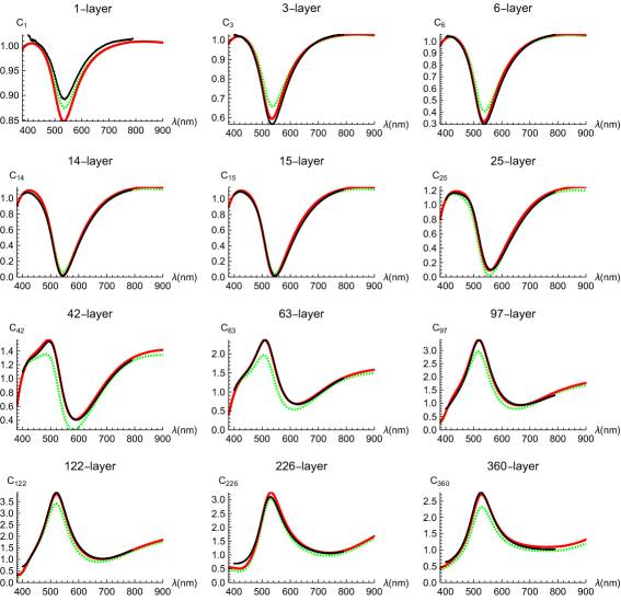
Multilayer graphene was prepared by exfoliating highly oriented pyrolytic graphite (HOPG) on the same SiO2/Si substrate. The reflectance of the multilayer graphene was measured with a spectroscopic reflectometer (TohoSpec3100, Toho Technology) using a objective lens. First, we determined that nm from the reflectance of the substrate (Appendix A). This value is used consistently in all the calculations reported in this paper, and it results in that destructive interference occurs for at nm. The thickness of the graphene flakes was determined by atomic force microscopy (Dimension XR, Bruker).
The representative measured spectral contrasts are depicted as black dots (circles) in Fig. 1 (The error bars for the data are within each circle). It is important to note that we present contrasts () instead of the reflectivities () to prevent any artificial shifts in the reflectivities (see Appendix A for more details). The general feature of the spectral shapes can be elucidated as follows: for thin samples with fewer than 40 layers, the contrast is subdued due to destructive interference from the substrate, resulting in a concave structure near nm. For thick samples with over 60 layers, is predominantly influenced by contributions from the -layer graphene and is minimally impacted by the substrate. Consequently, given that , suppressed by destructive interference, is in the denominator of the contrast, a convex structure appears near nm.
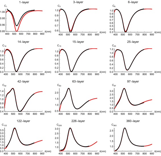
The contrasts, calculated using Eq. (1), are represented by the red solid curves in Fig. 1. A satisfactory fit with no significant deviations is achieved for various multilayer graphene samples, except for and . The observed discrepancy in these thin samples likely arises from differences in the interface between graphene and the substrate compared to that between adjacent graphene layers. This discrepancy is specific to thin samples and becomes negligible at 6 layers. The notable agreement between measured and calculated reflectance for visible light clearly indicates the following two facts. First, multilayer graphene can be treated as a collection of independent single layers, which is plausible since the effect of interlayer stacking does not manifest in the dynamical conductivity within the visible light range. Second, reflectance measurements provide a reliable value of layer number , averaged within a light spot. This is true even when the thickness of the graphene flakes determined by atomic force microscopy shows positional fluctuations to a certain extent. These facts will be used to validate the underlying assumption of our theoretical model of reflection presented in the subsequent sections.
and vanish at , which has been referred to as zero reflection. [29, 5] Zero reflection is useful in knowing the values of basic parameters later (at the end of Sec. III). To capture the essential role of graphene in achieving zero reflection, let us consider Eq. (1) when . For the numerator to vanish, has to be satisfied. Since is small, this equation can be simplified as , which shows that is an approximate layer number that gives zero reflection. This argument makes it easy to understand that the dominant imaginary part of is essential for zero reflection to occur.
II.3 Effective coupling constant
As the difference between the calculated and experimental values of contrasts proves to be sufficiently small for various multilayer graphene samples when utilizing the experimental values in Eq. (1), the optical constants [19] are the results that theory should ultimately elucidate. It can be inferred that nearly all the optical information of graphene multilayers is encompassed in the optical constant of monolayer graphene. This inference is partially attributed to the fact that the effect of the stacking order on the reflectance does not manifest in the visible regime. Consequently, we must inquire to what extent the theory of graphene optics can account for the and values.
Because of a conical energy-band structure of graphene known as the Dirac cone, the dynamical conductivity is well approximated by for visible light. [30] As a result, (suspended) monolayer graphene absorbs percent () of the incident visible light. [31] A straightforward calculation of the Kubo formula shows that the dynamical conductivity of graphite is given by that of graphene divided by the interlayer spacing ( nm): . [32, 20, 33] The reflectance in the visible regime is free from the effects of the stacking order, [34, 35, 36] Fermi energy position, and temperature at room temperature ranges. [37] Thus, the relative permittivity of graphite for visible light wavelengths is written as
| (2) |
where is the dielectric constant of the interlayer space.
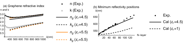
By equating the right-hand side of Eq. (2) with , we define an effective coupling constant , which is compared with in Fig. 2(a). The difference between and is actually larger than the order of 10 percent of which is beyond the level of small corrections of order of considered theoretically so far. Similarly, we define and plot it in Fig. 2(b). If the interlayer space is a vacuum, an appropriate choice of would be 1. However, is very different from unity because the electronic wave function of the -orbital spreads into the interlayer space, light propagating in it is subjected to the spread of the wave function. [38, 39] Fang et al. [38] calculate using a microscopic Poisson equation which has been tested by experiment. [39] The calculated effective dielectric thickness of graphene is found to be 0.22 nm, and the microscopic dielectric permittivity decays from 6.9 in the carbon-atom plane to the vacuum permittivity within approximately 0.1 nm. Though the calculation is for the electric field pointing in the direction perpendicular to the graphene sheet, similar (but slightly smaller) value is expected for the direction parallel to the sheet (let us assume it is here).

III Corrections to reflectance by light emission
A substantial correction to the dynamical conductivity is deemed impermissible because, if allowed, it would result in an inconsistency with the experimental observation that a (suspended) monolayer graphene absorbs approximately 2.3 percent () of the incident visible light. [31] An accurate theory capable of describing the reflectance does not necessitate corrections to dynamical conductivity but rather requires a mechanism that explains reflectance without altering . The model of light emission from graphene introduced in this section serves as an illustration of such a mechanism. Our model inherently incorporates the crucial concept of wave interference, specifically coherence or incoherence, as the initial phase of light emitted from each graphene layer.
III.1 Basic idea
Figure 3(a) illustrates our model of reflection, where horizontal lines on the substrate represent -layer graphene, and the vertical lines depict light rays with arrows indicating the directions of light propagation. The light rays on the left side (black in color) of Fig. 3(a) show the primary processes of reflection (excluding contributions from light emission). In this process, incident light from a light source is transmitted and reflected by graphene, while some energy of light being absorbed by each layer. The reflection coefficient, , is calculated from a primary model which is defined in Sec. III.2. The light rays on the right side (red in color) correspond to the light emission. Suppose that the th layer emits light. The emitted light is transmitted and reflected by graphene until the light escapes the system, and it contributes to the reflectance of the system. Thus, there is another “reflection coefficient” when -layer graphene emits light which is defined in Sec. III.3. Let denotes the sum over such amplitudes from all layers. Once we know what and are, then the reflectance is given by .
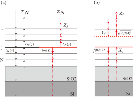
We use a transfer matrix method to calculate and . [20, 33] Transfer matrix method is useful in calculating reflection (up arrow) and transmission (down) coefficients at each layer [ and in Fig. 3(a)] in addition to the electric field () that determines the absorption of the th layer as . The total absorption of -layer graphene is . [20]
III.2 Primary model
Basically, primary model means the Fresnel equation of Eq. (1) where is given by Eq. (2). has a single unknown constant which can be estimated from the following observations. Ultimately, we conclude that .
First, there must not be a large discrepancy between and the experimentally determined optical constants. [40, 19] Experimental values for and [19] are shown as and in Fig. 4(a). The lines depict (bare) optical constants plotted using Eq. (2) with the refractive index and absorption coefficient for and 5.5. When , but has a certain difference from . When , but has a certain difference from . Because increases with increasing while decreases, there is no value that can reproduce and simultaneously. This suggests that there should be such a discrepancy between them which is attributed to the corrections by light emission. Second, has to roughly reproduce the behavior of the reflectance of multilayer graphene. It exhibits a minimum at a certain wavelength, primarily due to destructive interference caused by SiO2. As shown in Fig. 4(b), the position is red-shifted by increasing , indicating that even thin graphite samples significantly impact the light interference effect. When , the position changes little, and a sizable artificial shift in wavelength is needed to ensure consistency between theory and experiment, which cannot be explained as a correction. When , a small difference between theory and experiment still remains. However, as we show later, the corrections provide better agreement not only for the wavelengths giving minimum reflectivity but also for the minimum reflectivity values, thus accounting for the difference. Third, roughly reproduces the reflectivity of graphite in the infrared region. [41] Similar values have been used to reproduce the observed reflectivities of graphite and graphene. [40, 18, 19] We note that the value of is less than the magnitude of the imaginary part of , since visible light has a much longer (400800 nm) than , although is certainly a small quantity. The optical properties of multilayer graphene are thus characterized by the large imaginary part of .
III.3 Model of light emission
The corrections to the reflectance are the main subjects of this paper. [9, 10] Specifically, we consider corrections where some fraction of the energy absorbed by the th layer (of -layer graphene) is transferred to light emitted from that layer [see the right side of Fig. 3(a)]. The amplitude of the emitted light is assumed to be the square root of the layer absorption , [33] multiplied by the branching ratio, , i.e., , where means that the light emission is direction-independent along the -axis. Note that depends not only on and but also on and .
To examine how light emitted from the th layer affects the reflectance, we define two subsystems, as shown in Fig. 5(b): one is an isolated -layer graphene in the air; the other is -layer graphene on SiO2/Si substrate. Using the transfer matrix method, we can obtain the transmission and reflection coefficients of an isolated -layer graphene in the air [denoted as and ] and the reflection coefficient of -layer graphene on the SiO2/Si substrate [denoted as ]. [20, 33] Let the reflection coefficients be and and transmission coefficient be for the combined subsystems [see Fig. 5(b)]. These can be obtained by a self-consistent manner as follows. After calculating , we add it to of the incident light to the -layer graphene (in the air) as and recalculate and . Then, we add a new to of the light incident to the -layer graphene on the SiO2/Si substrate as and recalculate . These computations are repeated until and converge. In this way, we can obtain analytical expressions for the converged , , and for a given :
| (3) | |||
The “corrected” electric fields at an infinitesimal distance above and below the th layer become and , respectively. Self-consistency, whereby and , is therefore essential to ensuring that the corrected electric field is continuous at the th layer, which is a requirement of Maxwell equations. The corrected amplitude of the emitted light is written as
| (4) |
By comparing this with , we see that more accurate value of the amplitude of the emitted light is given by multiplying with as the renormalization constant, and is what in Fig. 3(a) represents. Therefore, we redefine as
| (5) | |||
| (6) |
We can interpret as follows. The transmission coefficient is the direct propagation of the renormalized light emitted from th layer to the air, and monotonously decreases with increasing . [20] The effects of scattering and absorption of the emitted light caused by surrounding layers is included by the part in the brace . It tends to suppress the magnitude of , but sometimes enhance. For example, when (i.e., monolayer on a substrate), the part becomes which is larger than unity when is positive.
is the value at zero initial phase, so the transmission coefficient can be given a phase degree of freedom expressing the coherence or incoherence of the light emission from the different layers:
| (7) |
Accordingly, the corrected reflectance is uniquely determined by . The value of depends on these phases . [42]
We consider a case in which the phase is given by a coherent phase. The exact derivation of the phase will be shown elsewhere because it is beyond the scope of the present paper. Here, we concisely explain the basic logic leading to the coherent phase in terms of quantum electrodynamics. First, we can define a quantum mechanical state of light () that the primary model describes (see left side of Fig. 3). All the information of light is expressed by the coefficients and (). Second, we can also define another quantum state of light () for the emitted light (see right side of Fig. 3). All the information of emitted light is expressed by the coefficients . These two states have an overlap caused by th layer graphene. Thus, if we consider a linear superposition of these states as to form energy eigenstates, the phase must be chosen so that becomes a real number, namely
| (8) |
The factor is a global phase () in the sense that it is independent of the value of . Because the scattered light () and the emitted light () form a two-level state, there are two possible linear superpositions of their energy eigenstates, () or (). The minus sign () is assigned to the lower energy state. From Eqs. (5) and (8), we obtain .
Including the correction due to coherent light emission leads to
| (9) |
where is the branching ratio of the energy of the emitted coherent photons to that of the absorbed photons. Since coherent photon emission is related to the electron-photon coupling strength of the annihilated photo-excited electron-hole pairs, should be on the order of and insensitive to changes in .
Next, we apply to the case that in is a random variable. Here, the definition of randomness is that if we take the time average regarding , we have and . We will refer to this case as incoherent corrections, which also include the cases that the global phase takes and if there is a perturbation that can mix the two energy levels. An interference term is now included in as the last term of
| (10) |
but it vanishes when taking the time average and only the first term of the incoherent corrections remains. [43] Inelastic scattering of light such as Raman scattering is usually considered to give rise to incoherent photons. Let be the branching ratio of the energy of the emitted incoherent photons to that of absorbed photons. Since is proportional to [Eq. (3)], the incoherent corrections are proportional to . For Raman scattering, the parameter is fundamentally determined by the electron-photon and electron-phonon coupling strengths, and it should not be so sensitive to the change in . Indeed, the incoherent corrections with a constant follow the measured dependence of the band Raman intensity [Sec. IV.3]. The band consists of optical phonons at the point, whose lattice vibrations are in-plane.
A generalized reflection formula covering the above two cases (coherent and incoherent corrections) can be written as
| (11) |
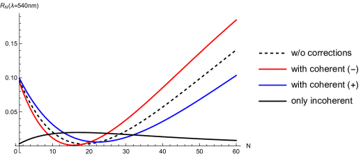
When , reduces to Eq. (1) with Eq. (2). Figure 5 shows the dependence of (dashed), (red), (blue), and (black), for a fixed nm. Note that the incoherent corrections always increase the reflectance and preclude zero reflections at , which is in contrast to the coherent corrections. Moreover, the band Raman intensity is enhanced when zero reflection occurs. [10, 44, 45, 46] This situation is called interference-enhanced Raman scattering, [9] and it is reasonably reproduced by Eq. (11). The experimental fact that zero reflection is observed at [see 14 and 15-layer in Fig. 1] shows that , is much smaller than 0.1, and (red curve in Fig. 5).
IV Applications of model
In this section, we show that the discrepancy between the measured reflectance of multilayer graphene [Fig. 1] and the prediction of the model [Eq. (11)] is sufficiently small for the present purpose. Our model is, therefore, nearly equivalent to the Fresnel equation with the experimental optical constants ( and ), [19] while our model can describe the interesting aspects of reflection. Using monolayer graphene, we provide a detailed explanation of the mechanism modifying the reflectance without introducing any artificial change in the dynamical conductivity. To showcase the versatility of our model, we also explore Raman scattering as incoherent corrections.
IV.1 Comparison of theory and experiment
Calculated contrasts are shown in Fig. 6 as red solid curves, which include coherent corrections only (i.e., ). Green dashed curves represent the primary model of Eq. (1), which does not include any corrections due to light emission. All calculations were performed with , where this value was chosen so that we could obtain good agreement between the calculations and observations for all layers. Note that this value is consistent with zero reflection being observed for .
From the consistency between the calculated and measured contrasts shown in Fig. 6 (except and ), we can draw two main conclusions. First, the phase () of the coherent corrections is essential. If we adopt 0 phase (), a serious discrepancy arises, as can be readily imagined from the relative location of the red solid curves with respect to the green dashed ones. Second, the incoherent corrections are rather small. In fact, for most of the layers examined (not shown in Fig. 6), the incoherent corrections did not improve the fitting. Our estimated reasonable range of is less than 0.01.
Only for the 226-layer, there is a slight but non-negligible deviation of the red solid curve from the measured contrast. A relatively small difference between the red solid and green dashed curves shows that the strength of is suppressed and that is under some special phase balance by interference for . Thus, a slight shift in might improve the fitting. For example, second order corrections which arise due to a self-consistent calculation of (and ) might be relevant to this.
IV.2 Monolayer
Unfortunately, the Fresnel equation is inconsistent with the measured contrast of monolayer graphene (see in Fig. 1), probably because reflectance depends on the condition of the interface between graphene and substrates. However, as we have carefully confirmed that almost all the information of the corrections from the emitted light is included in the reflectance of monolayer graphene, we believe that the contrast calculated from the Fresnel equation with the experimental and values is the result that we should compare with the model.
In Fig. 7(a), we present simulated (black dotted) and calculated (green dashed and red solid) spectral contrasts of monolayer graphene on the SiO2/Si substrate. Clearly, the corrections are of physical significance; black dots and red solid curve almost perfectly match. In , becomes a positive number only near as shown in Fig. 7(c). This is due to the destructive interference caused by SiO2, which also increases the absorption because . This enhanced absorption leads to the main difference between the reflectances from the substrate () and from the graphene on it (), increasing the visibility of graphene. The correction due to light emission is a negative number due to the negative global phase of an energetically stable configuration of light. Thus, the corrections increase . Namely, the increase in the visibility of graphene is mainly due to the substrate-induced enhancement of light absorption and is partly due to light emission.
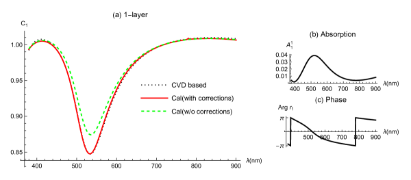
It is important to note that the primary model can explain the measured contrasts if is more than 20 percent larger than . However, this immediately leads to an inconsistency with the experimental fact that (suspended) monolayer graphene absorbs percent () of the incident visible light. [31] Additionally, the primary model with such corrections to does not reproduce the measured contrasts of many samples with different thickness. Furthermore, the primary model is not applicable to the Raman effect, while our model can include it in a natural way, as shown below.
IV.3 Raman scattering as incoherent corrections
We measured the band Raman peak intensity as a function of layer number in order to verify the interpretation of Raman scattering being an incoherent light emission. [10] The incoherent correction is defined by the last term of Eq. (11) as . is proportional to and does not depend on the value of when scaled. As shown in Fig. 8, there is a reasonable similarity between the measured Raman intensity (dots) and calculated incoherent component (dashed curve). Also plotted is an approximation of (dot-dashed curve) defined by
| (12) |
to show the effect of multiple scattering of incoherent light. The approximation overestimates the intensity for thick samples, as readily imagined.
On the other hand, there is a noticeable discrepancy between them for samples with fewer than 30 layers, where there is a dip in the reflectance that is similar to the observation by No et al. [46] The assumption of a random phase for in Eq. (7) is a possible reason for the discrepancy, because random phases can undergo synchronization or entrainment. [42] An intermediate state of the phase that is neither random nor perfectly coherent may account for the behavior.

V Discussion
There is a possibility that substrates play a decisive role in determining the selection of the two states specified by the global phase (0 and ). To see this, let us consider monolayer graphene suspended in the air. From Eq. (1), the reflection and transmission coefficients (without substrates) are and , and the absorption is given by . Light emission modifies the reflection coefficient as follows:
| (13) |
The magnitude of the second term is 0.0028 when which is about 25 percent the magnitude of the first term (0.011). The reflection increases or decreases depending on . When (0), the correction term is negative (positive) in sign; therefore, the light emission increases (decreases) the reflectance. Mathematically speaking, the change in the reflectance is equivalent to a replacement of as . This immediately leads to an inconsistency with the experimental fact that suspended monolayer graphene absorbs percent (, the measured uncertainty is within 5 percent of ) of the incident visible light. [31] This inconsistency is resolved by considering that for graphene suspended in the air the states of and 0 are degenerate and the effect of light emission effectively disappear by interference. This contrasts with monolayer graphene on SiO2/Si substrates for which is selected.
Since coherent and incoherent emissions are two extreme cases (uniform and random) of the phase in Eq. (7), a sharp distinction between the coherent and incoherent emissions is not always possible. The proper way to calculate the reflectance is to derive a dynamical model of at a microscopic level, [47, 42] and use it to calculate . Especially in the case of monolayer, they are inseparable as
| (14) |
when and have some correlation. Then, the reflectance is always subject to fluctuations created by the last term (through electron-phonon interactions).
Our model postulates that the effect of the emitted light appears as a correction to the reflection (and transmission) coefficient, not as a correction to the dynamical conductivity. Meanwhile, spontaneous emission is generally treated as a loss, and it is often included as a phenomenological relaxation constant in the dynamical conductivity. For example, in Ref 19, the authors introduce relaxation constants for Drude-Lorentz oscillator model to interpret the measured optical constants. However, an excessively large relaxation constant (or very short lifetime) for the Drude term (0.6 fs) already raises concerns about the naturalness of including such a relaxation parameter. [48] The justification of our postulate needs a theoretical clarification at a more fundamental level of quantum electrodynamics, which is capable of describing photon creation and annihilation, while the excellent agreement between the model and experiments clearly shows that this postulate works well. Our model is also consistent with a theoretical result that the dynamical conductivity is free from such a correction when graphene is undoped (i.e., charge neutrality condition is satisfied). [30] Moreover, the model explains the -dependence of the Raman intensity as the incoherent corrections (Sec IV.3), besides the contrast, in a unified manner.
VI Conclusion
In summary, we succeeded in explaining the measured visible contrasts of multilayer graphene samples on an SiO2/Si substrate by including coherent light emissions that come from some fraction () of the absorbed photon energy. The coherent corrections are essential for assuring the consistency between theory and experiment, while the incoherent corrections can be neglected for the contrast.
Photo-excited electrons contribute insignificantly to light emission when they are distant from the bottom of the conduction band. Namely, the value of for those electrons would be suppressed. In fact, graphene lacks a bandgap and the branching ratio of coherent light emission to absorbed light is very small (). What we have argued for in this paper is corrections (to the main effect) that have small branching ratios. However, whether light emission from those electrons can be entirely neglected depends on various factors. Graphene serves as an interesting example where corrections are greatly enhanced by its large absorption. The destructive interference effect from the substrate and the multilayer-induced coherence are the means by which it is observable in the reflectance. Similar emission-based corrections could be anticipated for other layered materials without band gaps, and the method developed here may prove useful in accurately understanding their optical properties.
Our formulation of the reflectance using the transfer matrix method has a descriptive ability for layered materials having defects and irregularities. For this reason, and considering the success it has had in describing the reflectance of relatively simple systems (graphene multilayer at visible range), we believe that some future form of this theory may be useful in describing the optical properties of any layered material with or without a band gap.
Acknowledgments
K. S thanks Y. Sekine, H. Endo, and Y. Taniyasu for raising helpful questions on this subject. Part of this work was supported by “Nanotechnology Platform Japan” of the Ministry of Education, Culture, Sports, Science and Technology (MEXT), Grant Number JPMXP09F21UT0045. The reflectance measurement was conducted in the Takeda Cleanroom with help of the Nanofabrication Platform Center of the School of Engineering, the University of Tokyo, Japan.
Appendix A Measured reflectivities
We performed the reflectivity measurements three times on the same sample (run 1, run 2, and run 3). All measurements were consistent in the sense that the measured reflectivities of -layer graphene on the substrate () divided by that of the SiO2/Si substrate (), that is, the contrast (), were identical. Therefore, we compared with calculations in the main text. However, while of run 2 and run 3 were identical, of run 1 deviated from that of run 2 (run 3), as shown in Fig. 9. The same contrast also means that the values of for run 2 and run 3 were identical, while for run 1 deviated from that of run 2 (run 3). The discrepancy between of run 1 and that of run 2 (run 3) was presumably brought about by a change in the focal point along the depth direction when a reference substrate was replaced with the target sample. This could change the incident light intensity and lead to a discrepancy in between run 1 and run 2 (run 3).
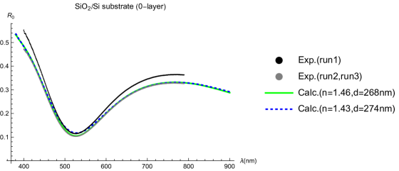
A problem arises when we determine the value of from . Considering that the wavelength giving the reflectivity minimum is the same for the three runs, we can determine nm by assuming that is the standard value (1.46). [28] These parameters reasonably reproduce of run 2 (run 3) [Fig. 9]. Meanwhile, 268 nm is inconsistent with another estimation using a reflectometer ( nm), which results in to reproduce the wavelength giving the reflectivity minimum by destructive interference (the same ). When we choose for nm, the corresponding is the (blue) dashed curve, which reproduces of run 1 around the reflectivity minimum (the two curves overlap from 460 to 560 nm) and approaches of run 2 (run 3) away from the reflectivity minimum ( nm and nm). Since is an acceptable value, we need to mindful of the possibility that a true is neither of run 1 nor that of run 2 (run 3). Because we have assumed that the refractive index of Si is the commonly used value, we keep the same standpoint for SiO2. Ultimately, we concluded that nm.
References
- Novoselov et al. [2005a] K. S. Novoselov, A. K. Geim, S. V. Morozov, D. Jiang, M. I. Katsnelson, I. V. Grigorieva, S. V. Dubonos, and A. A. Firsov, Nature 438, 197 (2005a).
- Zhang et al. [2005] Y. Zhang, Y.-W. Tan, H. L. Stormer, and P. Kim, Nature 438, 201 (2005).
- Novoselov et al. [2005b] K. S. Novoselov, D. Jiang, F. Schedin, T. J. Booth, V. V. Khotkevich, S. V. Morozov, and A. K. Geim, Proceedings of the National Academy of Sciences of the United States of America 102, 10451 (2005b).
- Blake et al. [2007] P. Blake, E. W. Hill, A. H. C. Neto, K. S. Novoselov, D. Jiang, R. Yang, T. J. Booth, and A. K. Geim, Applied Physics Letters 91, 063124 (2007).
- Roddaro et al. [2007] S. Roddaro, P. Pingue, V. Piazza, V. Pellegrini, and F. Beltram, Nano Letters 7, 2707 (2007).
- Ni et al. [2007] Z. H. Ni, H. M. Wang, J. Kasim, H. M. Fan, T. Yu, Y. H. Wu, Y. P. Feng, and Z. X. Shen, Nano Letters 7, 2758 (2007).
- Casiraghi et al. [2007] C. Casiraghi, A. Hartschuh, E. Lidorikis, H. Qian, H. Harutyunyan, T. Gokus, K. S. Novoselov, and A. C. Ferrari, Nano Letters 7, 2711 (2007).
- Ghamsari et al. [2016] B. G. Ghamsari, J. Tosado, M. Yamamoto, M. S. Fuhrer, and S. M. Anlage, Scientific Reports 6, 1 (2016).
- Nemanich et al. [1980] R. J. Nemanich, C. C. Tsai, and G. A. N. Connell, Physical Review Letters 44, 273 (1980).
- Wang et al. [2008] Y. Y. Wang, Z. H. Ni, Z. X. Shen, H. M. Wang, and Y. H. Wu, Applied Physics Letters 92, 043121 (2008).
- Stöhr et al. [2010] R. J. Stöhr, R. Kolesov, J. Pflaum, and J. Wrachtrup, Physical Review B 82, 121408 (2010), arXiv:1006.5434 .
- Lui et al. [2010] C. H. Lui, K. F. Mak, J. Shan, and T. F. Heinz, Physical Review Letters 105, 127404 (2010).
- Liu et al. [2010] W. T. Liu, S. W. Wu, P. J. Schuck, M. Salmeron, Y. R. Shen, and F. Wang, Physical Review B 82, 081408 (2010).
- Suemoto et al. [2013] T. Suemoto, S. Sakaki, M. Nakajima, Y. Ishida, and S. Shin, Physical Review B - Condensed Matter and Materials Physics 87, 10.1103/PhysRevB.87.224302 (2013).
- Riaz et al. [2015] A. Riaz, F. Pyatkov, A. Alam, S. Dehm, A. Felten, V. S. Chakravadhanula, B. S. Flavel, C. Kübel, U. Lemmer, and R. Krupke, Nanotechnology 26, 325202 (2015).
- Song et al. [2013] J. C. Song, K. J. Tielrooij, F. H. Koppens, and L. S. Levitov, Physical Review B - Condensed Matter and Materials Physics 87, 155429 (2013), arXiv:1209.4346 .
- Massicotte et al. [2021] M. Massicotte, G. Soavi, A. Principi, and K. J. Tielrooij, Hot carriers in graphene-fundamentals and applications (2021).
- Castriota et al. [2019] M. Castriota, G. G. Politano, C. Vena, M. P. De Santo, G. Desiderio, M. Davoli, E. Cazzanelli, and C. Versace, Applied Surface Science 467-468, 10.1016/j.apsusc.2018.10.161 (2019).
- El-Sayed et al. [2021] M. A. El-Sayed, G. A. Ermolaev, K. V. Voronin, R. I. Romanov, G. I. Tselikov, D. I. Yakubovsky, N. V. Doroshina, A. B. Nemtsov, V. R. Solovey, A. A. Voronov, S. M. Novikov, A. A. Vyshnevyy, A. M. Markeev, A. V. Arsenin, and V. S. Volkov, Nanomaterials 2021, Vol. 11, Page 1230 11, 1230 (2021).
- Sasaki and Hitachi [2020] K. Sasaki and K. Hitachi, Communications Physics 3, 90 (2020).
- Hendry et al. [2010] E. Hendry, P. J. Hale, J. Moger, A. K. Savchenko, and S. A. Mikhailov, Physical Review Letters 105, 097401 (2010).
- Sun et al. [2010] Z. Sun, T. Hasan, F. Torrisi, D. Popa, G. Privitera, F. Wang, F. Bonaccorso, D. M. Basko, and A. C. Ferrari, ACS Nano 4, 803 (2010), arXiv:0909.0457 .
- Mikhailov [2012] S. A. Mikhailov, Physica E: Low-dimensional Systems and Nanostructures 44, 924 (2012).
- Yang et al. [2018] H. Yang, H. Guan, N. Biekert, G. Arefe, D. C. Chang, Y. Sun, P. C. Yeh, X. Liu, S. Y. Hong, I. D. Marion, M. Kralj, J. C. Hone, R. M. Osgood, and J. I. Dadap, Physical Review Materials 2, 071002 (2018).
- Stauber et al. [2008] T. Stauber, N. M. R. Peres, and A. K. Geim, Physical Review B 78, 085432 (2008).
- Stauber et al. [2017] T. Stauber, P. Parida, M. Trushin, M. V. Ulybyshev, D. L. Boyda, and J. Schliemann, Physical Review Letters 118, 10.1103/PhysRevLett.118.266801 (2017).
- Aspnes and Studna [1983] D. E. Aspnes and A. A. Studna, Physical Review B 27, 985 (1983).
- Malitson [1965] I. H. Malitson, J. Opt. Soc. Am. 55, 1205 (1965).
- Anders [1965] H. Anders, Thin Films in Optics (The Focal Press, 1965).
- Ando et al. [2002] T. Ando, Y. Zheng, and H. Suzuura, Journal of the Physical Society of Japan 71, 1318 (2002).
- Nair et al. [2008] R. R. Nair, P. Blake, A. N. Grigorenko, K. S. Novoselov, T. J. Booth, T. Stauber, N. M. R. Peres, and A. K. Geim, Science 320, 1308 (2008).
- Kuzmenko et al. [2008] A. B. Kuzmenko, E. van Heumen, F. Carbone, and D. van der Marel, Physical Review Letters 100, 117401 (2008).
- Sasaki [2020] K.-i. Sasaki, Journal of the Physical Society of Japan 89, 094706 (2020).
- Taft and Philipp [1965] E. A. Taft and H. R. Philipp, Physical Review 138, A197 (1965).
- Ichikawa and Kobayashi [1966] Y. H. Ichikawa and K. Kobayashi, Carbon 3, 401 (1966).
- Dresselhaus and Dresselhaus [1976] M. S. Dresselhaus and G. Dresselhaus, Physical Review B 13, 4635 (1976).
- Klimchitskaya et al. [2018] G. L. Klimchitskaya, V. M. Mostepanenko, and V. M. Petrov, Physical Review A 98, 023809 (2018).
- Fang et al. [2016] J. Fang, W. G. Vandenberghe, and M. V. Fischetti, Physical Review B 94, 045318 (2016).
- Rickhaus et al. [2020] P. Rickhaus, M. H. Liu, M. Kurpas, A. Kurzmann, Y. Lee, H. Overweg, M. Eich, R. Pisoni, T. Taniguchi, K. Watanabe, K. Richter, K. Ensslin, and T. Ihn, Science Advances 6, 10.1126/sciadv.aay8409 (2020).
- Bruna and Borini [2009] M. Bruna and S. Borini, Applied Physics Letters 94, 031901 (2009).
- Djurišić and Li [1999] A. B. Djurišić and E. H. Li, Journal of Applied Physics 85, 7404 (1999).
- Kuramoto [1984] Y. Kuramoto Springer Series in Synergetics, 19, 10.1007/978-3-642-69689-3 (1984).
- Velson et al. [2020] N. V. Velson, N. V. Velson, H. Zobeiri, X. Wang, and X. Wang, Optics Express, Vol. 28, Issue 23, pp. 35272-35283 28, 35272 (2020).
- Yoon et al. [2009] D. Yoon, H. Moon, H. Cheong, J. S. Choi, J. A. Choi, and B. H. Park, Journal of the Korean Physical Society 55, 1299 (2009).
- Li et al. [2015] X. L. Li, X. F. Qiao, W. P. Han, Y. Lu, Q. H. Tan, X. L. Liu, and P. H. Tan, Nanoscale 7, 8135 (2015).
- No et al. [2018] Y. S. No, H. K. Choi, J. S. Kim, H. Kim, Y. J. Yu, C. G. Choi, and J. S. Choi, Scientific Reports 8, 1 (2018).
- Dicke [1954] R. H. Dicke, Physical Review 93, 99 (1954).
- Toqeer et al. [2021] I. Toqeer, M. Z. Yaqoob, A. Ghaffar, M. A. S. Alkanhal, Y. Khan, and Y. T. Aladadi, Journal of the Optical Society of America A 38, 10.1364/josaa.412649 (2021).