Eavesdropping on competing condensates by the edge supercurrent in a Weyl superconductor
In a topological insulator the metallic surface states are easily distinguished from the insulating bulk states [1]. By contrast, in a topological superconductor [2, 3, 4, 5], much less is known about the relationship between an edge supercurrent and the bulk pair condensate. Can we force their pairing symmetries to be incompatible? In the superconducting state of the Weyl semimetal MoTe2, an edge supercurrent is observed as oscillations in the current-voltage (I-V) curves induced by fluxoid quantization [6]. We have found that the -wave pairing potential of supercurrent injected from niobium contacts is incompatible with the intrinsic pair condensate in MoTe2. The incompatibility leads to strong stochasticity in the switching current as well as other anomalous properties such as an unusual antihysteretic behavior of the “wrong” sign. Under supercurrent injection, the fluxoid-induced edge oscillations survive to much higher magnetic fields H. Interestingly, the oscillations are either very noisy or noise-free depending on the pair potential that ends up dictating the edge pairing. Using the phase noise as a sensitive probe that eavesdrops on the competiting bulk states, we uncover an underlying blockade mechanism whereby the intrinsic condensate can pre-emptively block proximitization by the Nb pair potential depending on the history.
Preliminaries
As reported in Ref. [6], the edge supercurrent in MoTe2 realizes a toroidal topology despite the absence of holes in the exfoliated crystals. As is slowly increased, fluxoid quantization leads to a sawtooth field profile for the edge superfluid velocity , which translates to oscillations of that are clearly seen in a color-map plot of vs. (a fluxoid is a flux quantum plus the superfluid circulation; Sec. VI in Supplementary Materials SM). The large number of oscillation cycles () allow its phase noise to be analyzed. The analysis reveals that a large phase noise appears whenever edge-state pairing, driven by Nb, is incompatible with bulk-state pairing in MoTe2. Incompatibility between the injected -wave supercurrent and paired states intrinsic to MoTe2 has observable consequences in both the bulk and edge states. By varying the contact geometry across 8 devices, we can distinguish edge-state features from those in the bulk.
Because the interfaces between Nb and MoTe2 have high transmittivity at 20 mK, our experiment lies in the strong-coupling proximity-effect regime, well beyond the Josephson effect regime (Sec. V in SM). In strong coupling junctions, the system (Nb plus MoTe2) is treated as a single superconductor with a unique and a gap function that is inhomogeneous [7, 8, 9, 10, 11, 12]. In device , ( mK) lies well above the unperturbed of pristine MoTe2 (100 mK) although still far below that of Nb ( K). Similarly, the critical field and critical current are greatly enhanced over the values in pristine MoTe2.
To discuss the proximity effect (Sec. VII of SM) [7, 8, 9, 10, 11, 12], we denote the Gor’kov pair amplitude in Nb by where annihilates an electron in spin state at . We call the pair amplitude in pristine MoTe2 (of unknown symmetry) . Aside from MoTe2, evidence for edge supercurrents has been reported in Bi nanowires [13] and in a Kagome superconductor [14].
Anti-hysteretic behavior of central peak
Figure 1a shows the color map of the differential resistance versus and current measured in device at temperature mK. In weak , supercurrent injection from Nb leads to a large critical current within a narrow central peak (shown shaded black) that reaches values of A (20 larger than seen in pristine crystals). An immediate surprise is the anomalous position of the central peak. In conventional superconductors, we expect to cross zero before the flux density does. Instead, the central peak here emerges before reaches zero for either scan (which seems oddly anti-causal). We dub this curious pattern “anti-hysteretic.”
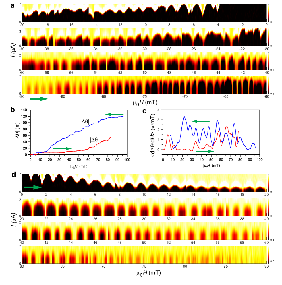
When exceeds 10 mT, we observe a dense array of periodic peaks in the color map (Figs. 1b and 1c). These are the fluxoid-induced oscillations [6], now persisting to 90 mT (compared with 3 mT in pristine crystals). As shown in Figs. 1d and 1e, the oscillations appear as narrow peaks in the differential resistance measured at . At each peak, reverses direction to admit a fluxoid [6].
Stochastic Switching
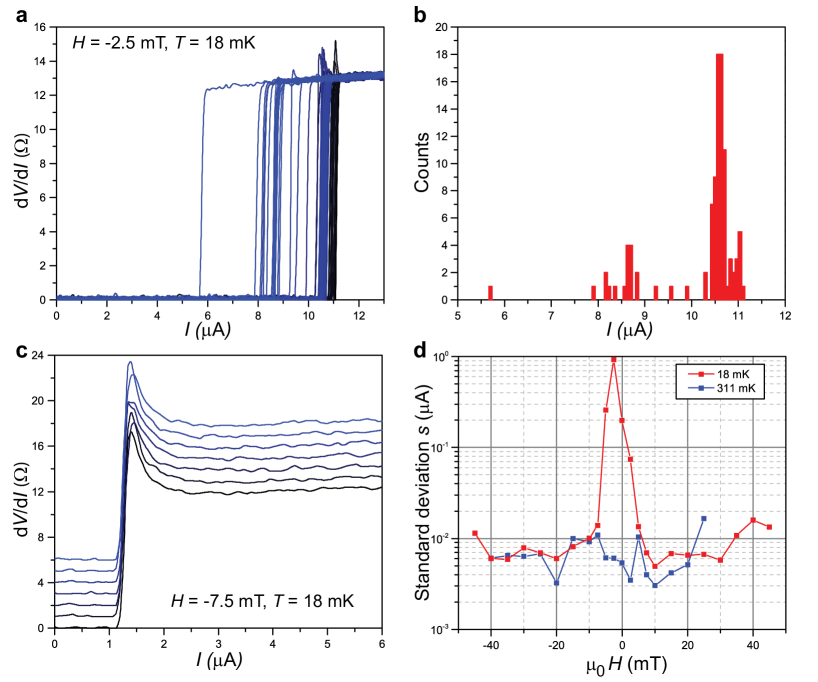
The incompatibility between the intrinsic pair condensation amplitude and injected from Nb is most evident in - curves measured when lies within the central peak in Fig. 1a. The switching transition is strongly stochastic (Sec. II in SM). In Fig. 2a, we plot 100 curves of vs. measured at 18 mK in device with fixed at mT. The critical currents obey a distribution function that is distinctly bimodal, with a histogram that shows a major peak at A and a minor one at 8.5 A (see Fig. 2b and Sec. II in SM). In the color map of (Fig. 1a), the stochastic nature of the distribution is also apparent as random spikes within the central peak.
By contrast, outside the central peak ( mT), the distribution becomes very narrow (Fig. 2c). The standard deviation (obtained from 100 scans at each ) is plotted in Fig. 2d. The profile displays a narrow peak at the central peak with peak value 100 larger than the baseline (red curve). At 311 mK, however, the peak is absent (blue curve).
The stochastic switching reflects the competition between bulk-date pairing with symmetry or .
Phase Noise and Anti-hysteretic Curves
The competition between and has a strong effect on the phase noise of the oscillations in . Field scans are called inbound if decreases with time, and outbound if increases.
On inbound branches (Figs. 1b and 1d), the noise content of the oscillations is invariably very large, whereas, on outbound branches (Figs. 1c and 1e), the phase noise is conspicuously suppressed, especially in the interval mT, which we call the “quiet” zone.
In Fig. 3 we emphasize the differences by displaying the color map of the oscillations over the entire field range. On the inbound branch (Fig. 3a), the noise content is much higher than on the outbound (Fig. 3d). To quantify the phase noise, we express the fluctuations in the frequency as an -dependent phase (Sec. III in SM). It is expedient to subtract from a background derived from an -linear fit to in the quiet zone (5, 45) mT (Sec. III in SM). The deviation then highlights field intervals with large phase noise. In Fig. 3b, on the inbound branch (blue curve) is seen to be much larger than on the outbound curve (red). In the quiet zone (5, 45) mT, is flat by design. We also employ the smoothed derivative which is more sensitive to local changes in the frequency. As seen in Fig. 3c, is much larger on the inbound branch than in the quiet zone on the outbound.
Aside from the oscillations, also displays a dissipationless regime bracketed by the two fields and (red arrows in Figs. 1d and 1e). An expanded view of these transitions is shown in Figs. 4a – 4h for 4 devices. In device , the transition on the inbound branch occurs at mT, larger in magnitude than the field (= 28 mT) on the outbound branch (blue curves in Fig. 4e). The reverse sweep (red curves) is the mirror reflection of the blue curve. The resulting hysteresis is again anti-hysteretic.
Distinguishing Edge from Bulk Supercurrents
The observed supercurrents segregate into two groups. In group I (central peak in Fig. 1a), attains very large values (A) but is easily suppressed in a weak ( mT). The second group (II) are the weak supercurrents (A) seen in the oscillations in which survive to fields up to 90 mT (Figs. 1 and 3).
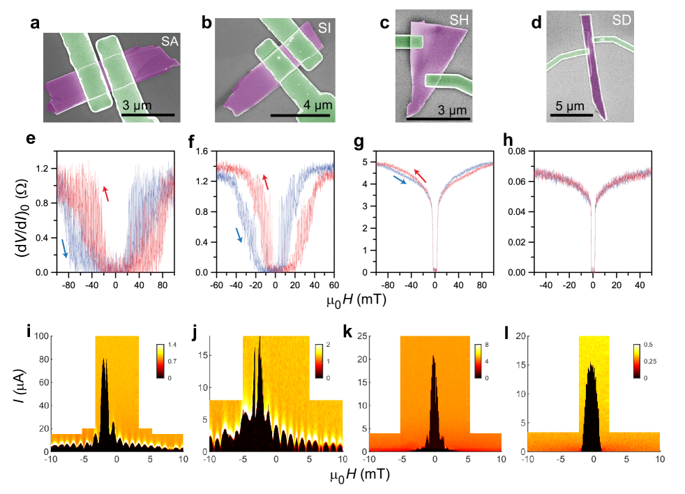
By tailoring the contact designs in 8 devices, we have found that the group II features are specific to edge states. The oscillation period corresponds to a fluxoid area bracketed by the Nb contacts (Sec. I in SM). Its perimeter is comprised of two segments (length ) lying under Nb contacts, and two segments called “links” (of length and ) at the uncovered physical edges (inset in Fig. 1a).
In five devices () the Nb contacts are laid down as parallel strips with spacing (Table S1, Fig. 4 and Fig. S3 in SM). In the remaining three (), the Nb contacts are progressively reduced in volume while and are greatly lengthened. These changes strongly attenuate group II features.
In Fig. 4, we show two parallel-strip devices, and (Panels a and b, respectively), and two devices, and , in the second series (c and d, respectively). The corresponding curves are displayed in Figs. 4e-4h, together with the color maps in Figs. 4i-4j. Group II features are prominently seen in and where we have . As we increase , the widths of the antihysteretic loops decrease. In devices (with = 5,420 and = 5,710 nm) and ( = 8,030 nm and = 17,670 nm), the edge oscillations and antihystereses are completely suppressed (aside from residual wings in ). Data from 4 other samples are shown in Fig. S3 in SM.
In devices and , supercurrent in the bulk flows in parallel with supercurrent in the links if is weak. When exceeds 4 mT, the bulk supercurrent is suppressed but the link supercurrents survive to large because they are one-dimensional. The robustness enables fluxoid oscillations to be observed up to 90 mT. To realize this, however, we need and to be shorter than the decay length ( nm) that governs the decay of the pair amplitude along a link (inset in Fig. 1a). If , (the case in SH and SD), decays to zero before the loop is closed, and the oscillations vanish (Fig. 4g,h). The vanishing of the closed-loop supercurrent is also evident in vs. , which stays finite except when 2 mT. These findings establish that the group II features arise from edge supercurrents at the links.
By comparison, the much larger values of the group I supercurrents (central peak in Fig. 1a) suggest a bulk origin. The 20-fold decrease in the peak value as increases from 156 to 700 nm also implies bulk states proximitized by (Table S1 in SM). The decrease is consistent with the short coherence length of Nb ( 40 nm). By contrast, at the links, .
Proximity Effect Between Competing Symmetries
In de Gennes’ treatment of the proximity effect (valid in the linear-gap regime) the amplitude for a Cooper pair to propagate between points and is given by the kernel [7, 9, 12] (Sec. VII in SM). Whenever a propagator segment lies in Nb, gains a large enhancement from the strong -channel attraction. Hence the gap function in MoTe2 can adopt either the symmetry of or that of depending on the weighted contributions of propagators going from all points (Eq. S23 in SM). An applied field can tip the balance by selectively weakening one or the other condensation amplitude. Calculations beyond the linear-gap regime show how the gap function changes symmetry in a junction between an - and a -wave superconductor [10].
At , the weighted average favors . Vortices inserted by initially form a vortex solid. With increasing , melting of the vortex solid leads to a dissipative vortex liquid in which the gap modulus remains finite but its phase fluctuates strongly due to vortex motion. In the vortex liquid, which survives to 80 mT, the loss of long-range phase coherence substantially weakens the pair amplitude relative to . Conversely, solidification of the vortex system strongly tilts the competition towards the intrinsic .
Correlating central peak, phase noise and antihysteresis
In each device, edge-state pairing at the links may be driven either by or from the nearest Nb contact. From the phase noise analysis, we infer that compatibility between edge-pairing and bulk-pairing produces oscillations that are nearly noise-free. By contrast, incompatibility between -wave pairing at the edge and in the bulk generates substantial phase noise.
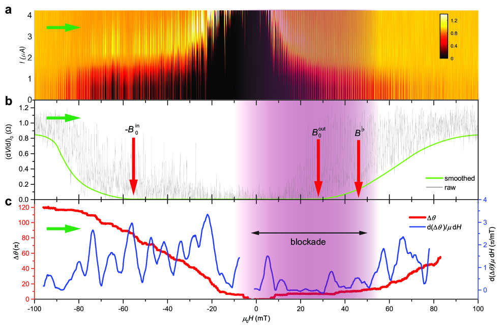
Combining the group I and II features with the phase noise measured by and in device , we arrive at a consistent picture of the antihysteretic behavior. The color map of and the trace of at 18 mK are displayed in Figs. 5a and b, respectively. Starting at mT, the phase noise is initially small, as seen in (blue curve in Fig. 5c). This implies that edge pairing is driven by the Nb contacts while all pairing of bulk states is strongly suppressed. When reaches mT, we observe a surge onset in phase noise which we take as evidence for incompatibility with the vortex liquid that appears at mT. The phase noise remains large over the entire interval (, ) mT (red curve in 5c).
When crosses mT, proximitization of the bulk states driven by becomes strongly favored ( becomes too weak to depair the bulk -wave condensate). The abrupt emergence at mT of a large bulk supercurrent (the central peak) signals when switches to -wave pairing (Figs. 5a), but this favorable interval is brief. When reaches mT, solidification of the vortex liquid (and the ensuing long-range phase coherence) cause to switch back to the intrinsic pairing symmetry . Suppression of all -wave paired regions throughout the crystal collapses the central peak before reaches 0-. Hence the placement of the central peak is antihysteretic as observed.
Blockade
When the field crosses zero to the outbound branch (), we should expect to see the re-appearance of the central peak in the interval (2, 4) mT. However, this is not observed in any of the 8 devices studied.
Together, the absence of the central peak for and the noise suppression in the interval mT suggest a “blockade” mechanism. Once switches to the intrinsic symmetry in the limit , the intrinsic condensate appears to block re-proximitization of the bulk by on the outbound branch throughout the quiet zone which extends to a field that we call 45 mT (shaded lilac in Figs. 5a-c). Edge pairing by Nb is blocked within the quiet zone.
The identification of with supercurrents at the edge clarifies considerably the anti-hysteretic loops in Figs. 4e and 4f. As shown by the green curve in Fig. 5b, the dissipationless interval for the edge current spans the interval mT for a left-to-right field scan. The interval is shifted left because, on the inbound branch, the edges are proximitized by the strong Nb pair potential, whereas, on the outbound, edge pairing is driven by the much weaker while -pairing is excluded by the blockade. Likewise, in a right-to-left scan, is shifted right. This accounts for the anti-hysteretic sign of the loops in .
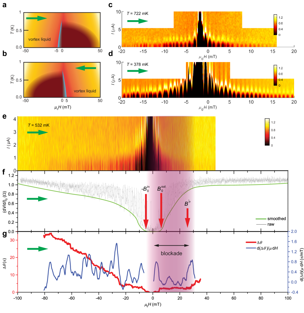
Raising the temperature
Figure 6a shows the blockade region (shaded maroon) inferred from left-to-right field scans taken at elevated temperatures 378, 532 and 722 mK (Fig. 6b is for the opposite field scan). The corresponding color maps of are displayed in Figs. 6c, d and e. For the results at 522 mK, we also show the trace of (Fig. 6f) and the phase noise measured by and (Fig. 6g). The overall patterns are similar to those taken at 18 mK (Fig. 5) except that raising decreases the field scales. The asymmetry of the phase noise, including its suppression in the blockade interval, is apparent in Figs. 6f and 6g. We find that the widths of the antihysteretic loops in , the edge dissipationless interval and all decrease systematically as increases, reaching zero at the device mK. The linear decrease of as is shown in Fig. S9. These trends are consistent with the key role played by in generating the antihysteresis, phase noise and the blockade.
Hysteretic solid-to-liquid transition
If we inspect the blockade region in the - plane (shaded maroon in Figs. 6a,b), we find that its placement mimics that of a vortex solid phase that is field-shifted by hysteresis. We conjecture that the blockade mechanism and quiet zone are features intrinsic to the vortex solid. If is swept from left to right (Fig. 6a), the liquid-to-solid transition is “delayed” on the inbound branch until reaches mT, analogous to supercooling of a liquid (regarding as an effective temperature). On the outbound branch, the solid-to-liquid transition is also delayed and shifted to 45 mT. Hence the observed vortex solid phase is displaced to the right as shown in Fig. 6a. For the opposite scan, the shift is to the left. We note that the supercooling hysteresis has the conventional sign. However, the blockade mechanism and incompatibility between condensates together displace the bulk and edge supercurrent responses in the opposite direction, which leads to the antihysteresis.
References
- [1] Liang Fu and C. L. Kane, Topological insulators with inversion symmetry, Phys. Rev. B 76, 045302 (2007).
- [2] Liang Fu and C. L. Kane, Superconducting Proximity Effect and Majorana Fermions at the Surface of a Topological Insulator, Phys. Rev. Lett. 100, 096407 (2008). DOI: 10.1103/PhysRevLett.100.096407
- [3] Xiao-Liang Qi, Taylor L. Hughes, S. Raghu and Shou-Cheng Zhang, Time reversal invariant topological superconductors and superfluids in two and three dimensions, Phys. Rev. Lett. 102, 187001 (2009). DOI: 10.1103/PhysRevLett.102.187001
- [4] Liang Fu and Erez Berg, Odd-parity topological superconductors: theory and application to CuxBi2Se3. Phys. Rev. Lett. 105, 097001 (2010). DOI: 10.1103/PhysRevLett.105.097001
- [5] Yang Peng, Falko Pientka, Erez Berg, Yuval Oreg, and Felix von Oppen, Signatures of topological Josephson junctions, Phys. Rev. B94, 085409 (2016). DOI: 10.1103/PhysRevB.94.085409
- [6] Wudi Wang, Stephan Kim, Minhao Liu, F. A. Cevallos, R. J. Cava, and N. P. Ong, Evidence for an edge supercurrent in the Weyl superconductor MoTe2, Science 368, 534-537 (2020). 10.1126/science.aaw9270
- [7] P. G. de Gennes, Boundary effects in superconductors, Rev. Mod. Phys. 36, 235 (1964).
- [8] P. G. de Gennes, Superconductivity of Metals and Alloys (Addison Wesley, 1989), Ch. 7.
- [9] G. Deutscher and P. G. de Gennes, Proximity Effects, in Superconductivity, Vol. II ed. Parks (Taylor and Francis 1969), Ch. 17.
- [10] B. Ashauer, G. Kieselmann and D. Rainer, On the proximity effect in unconventional superconductors, J. Low Temp. Phys. 63, 349 (1986).
- [11] A. Millis, D. Rainer and J. A. Sauls, Quasiclassical theory of superconductivity near magnetically active interfaces, Phys. Rev. B 38, 4504 (1988).
- [12] Manfred Sigrist and Kazuo Ueda, Phenomenological theory of unconventional superconductivity, Rev. Mod. Phys. 63, 23 (1991).
- [13] Anil Murani, Alik Kasumov, Shamashis Sengupta, Yu A. Kasumov, V.T. Volkov, I.I. Khodos, F. Brisset, Raphaelle Delagrange, Alexei Chepelianskii, Richard Deblock, Helene Bouchiat and Sophie Gueron, Ballistic edge states in Bismuth nanowires revealed by SQUID interferometry, Nat. Commun. 8, 15941 (2017). doi: 10.1038/ncomms15941.
- [14] Yaojia Wang, Shuo-Ying Yang, Pranava K. Sivakumar, Brenden R. Ortiz, Samuel M.L. Teicher, Heng Wu, Abhay K. Srivastava, Chirag Garg, Defa Liu, Stuart S. P. Parkin, Eric S. Toberer, Tyrel McQueen, Stephen D. Wilson, Mazhar N. Ali, Proximity-induced spin-triplet superconductivity and edge supercurrent in the topological Kagome metal, K1-xV3Sb5, cond-mat arXiv: 2012.05898.
* * *
§Corresponding author email: npo@princeton.edu
Data availability
The data in the plots will be uploaded to Harvard DataVerse.
Acknowledgements
We have benefitted from discussions with Wudi Wang and Zheyi Zhu. N.P.O. and S.K. were supported by the U.S. Department of Energy (DE-SC0017863).
The crystal growth effort was supported by a MRSEC grant from the U.S. National Science Foundation (NSF DMR-2011750) which supported S.L, L.M.S., R.J.C and N.P.O. The Gordon and Betty Moore Foundation’s EPiQS initiative provided generous support via grants GBMF9466 (N.P.O.) and GBMF9064 (L.M.S.).
Author contributions
S.K. and N.P.O. conceptualized and designed the experiment. S.K. performed all device fabrication and measurements. The crystals were grown by S.L., L.M.S. and R.J.C. Analysis of the data were carried out by S.K. and N.P.O. who jointly wrote the manuscript.
Competing financial interests
The authors declare no competing financial interests.
Additional Information
Supplementary Materials is available in the online version of the paper.
Correspondence and requests for materials should be addressed to N.P.O.

Methods
I Device fabrication
The MoTe2 devices were fabricated following standard nanofabrication procedures. Substrates with pre-patterned alignment makers were prepared in advance. The alignment markers were made of 5 nm of Ti and 50 nm Au. MoTe2 microflakes were mechanically exfoliated on to the substrates using Nitto Denko SPV 5057A5 Surface Protection Tape. Microflakes with adequate sizes with sharp edges were chosen using an optical microscope.
Niobium electrodes were made following the standard PMMA-copolymer bilayer recipe. After the resists were spun on top of substrates, contacts were patterned using EBPG 5150 from Raith. The devices were developed with MIBK-IPA (1:3) solution for 60 seconds and rinsed with IPA solution. The devices were then transferred to an EvoVac Sputtering System (Angstrom Engineering). An in-situ Ar plasma beam bombarded the surfaces of the devices for 120 seconds to remove the top few layers of MoTe2 that were oxidized. A thin layer (3 nm) of Ti layer was sputtered at a rate nm/s to form a sticking layer, followed by 100 nm of Nb deposited at a rate 1 nm/s. Finally, a 5 nm of Au was sputtered on top of Nb layer to protect it from oxidization. All sputtering procedures were performed at a high vacuum of approximately mbar.
II Measurement techniques
Measurements were carried out in a top-loading dilution refrigerator (Oxford Instruments Kelvinox TLM). Once loaded to the fridge, devices were immersed in the circulating 3He-4He mixture in the mixing chamber. The base temperature of the fridge was mK. Three filters were used to reduce noises during measurements. An -filter, located at the top of the probe, provided 80-dB suppression for frequencies MHz. The two other filters were located in the mixing chamber. The first one was a sintered metal powder filter that consisted of Cu particles of 30-60 in diameter. It suppressed any stray electromagnetic radiation for frequencies GHz. The second filter was a low-pass filter with the cutoff frequency of kHz. A NbTi superconducting magnet was used to apply magnetic fields to devices. A Keithley 2400 and a Keithley 6221 provided the current to superconducting magnet. The smallest field-step size was as small as a few T.
Differential resistances of all devices were measured using a SR830 lock-in amplifier. A DC bias from a Keithley 2400 voltage source was superposed with a small AC excitation voltage from the lock-in amplifier through a home-made voltage adder. The resulting voltage was converted to current through a buffer resistor that was orders of magnitude larger in resistance than the device of interest. The voltage signal across the device first passed through a pre-amplifier to improve the signal-to-noise ratio. The gain was usually in the order of . The amplified signal then reached the lock-in amplifier for detection. Measurements were done in quasi-4-point fashion. Although both voltage and current contacts shared the same electrodes, the electrodes were superconducting at 20 mK.
The differential resistance plots in the main text were obtained through the following procedures: first, the magnetic field was set to the desired value. Then the DC bias was ramped from zero to the desired bias value with a small step size. After reaching the desired bias, the current was ramped back to zero with a much larger step size. Such procedures were repeated for desired field ranges. The collected differential resistance curves were plotted together. The differential resistance versus field at zero bias plots were prepared as follows: starting with the field at zero, we swept to its maximum negative value then to the maximum positive value before terminating at zero.