A 23 W Keyword Spotting IC with Ring-Oscillator-Based Time-Domain Feature Extraction
Abstract
This article presents the first keyword spotting (KWS) IC which uses a ring-oscillator-based time-domain processing technique for its analog feature extractor (FEx). Its extensive usage of time-encoding schemes allows the analog audio signal to be processed in a fully time-domain manner except for the voltage-to-time conversion stage of the analog front-end. Benefiting from fundamental building blocks based on digital logic gates, it offers a better technology scalability compared to conventional voltage-domain designs. Fabricated in a 65 nm CMOS process, the prototyped KWS IC occupies 2.03mm2 and dissipates 23 W power consumption including analog FEx and digital neural network classifier. The 16-channel time-domain FEx achieves 54.89 dB dynamic range for 16 ms frame shift size while consuming 9.3 W. The measurement result verifies that the proposed IC performs a 12-class KWS task on the Google Speech Command Dataset (GSCD) with 86% accuracy and 12.4 ms latency.
Index Terms:
Analog, band-pass filter (BPF), classifier, feature extractor (FEx), Google Speech Command Dataset (GSCD), keyword spotting (KWS), rectifier, recurrent neural network (RNN), ring-oscillator, time-domain.I Introduction
With incredible advances in Artificial Intelligence (AI) fields, there is an increasing demand for low-power audio Internet of Things (IoT) devices that process human speech on the device without data transmission to the cloud. These smart devices are required to ensure always-on operation, real-time response, small form factor, and longer battery lifetime. As such, an ultra-low-power wake-up functionality is being highlighted with rapidly growing popularity because it allows hierarchical power gating of increasingly complex tasks for audio \pdftooltipIoTInternet of Things nodes. Keyword Spotting (KWS) and Voice Activity Detection (VAD) are widely used user-interactive methods to wake-up smart devices. \pdftooltipKWSKeyword Spotting is used to detect predefined keywords in an audio stream while \pdftooltipVADVoice Activity Detection detects when a human voice is present.
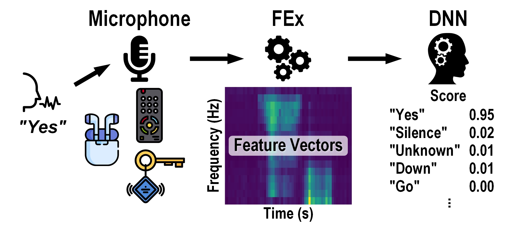
Fig. 1 shows the typical processing stages for \pdftooltipKWSKeyword Spotting. The user says a keyword into the microphone of an edge device such as a remote control or wireless earbud. The microphone output is further processed by a Feature Extractor (FEx) which generates frequency-selective Feature Vectors (FVs) that are continuously streamed to a Deep Neural Network (DNN)-based classifier. The classifier outputs the probability scores of different keywords. \pdftooltipIoTInternet of Things devices benefit from a tiny form factor and the use of a small battery such as a coin cell, e.g., for smart tags. Generally a 100 W system-level power is desirable including not only the \pdftooltipKWSKeyword Spotting IC itself but also the microphone and other system components. Moreover, a low-latency response is desired considering a \pdftooltipKWSKeyword Spotting-driven hierarchical processing system used in an interactive environment. For example, a study on the perception of self-generated speech showed that a delay exceeding 20 ms becomes disturbing for users [1].

A 12-class \pdftooltipKWSKeyword Spotting IC that includes the whole processing chain starting from the Analog-to-Digital Converter (ADC) to the \pdftooltipDNNDeep Neural Network classifier [2] reported that the \pdftooltipFExFeature Extractor is the most power-hungry stage accounting for 40% of the power dissipation in the entire IC. To reduce the power budget of edge devices thereby facilitating longer battery lifetime or smaller battery size, various circuit design techniques have been proposed for both \pdftooltipKWSKeyword Spotting and \pdftooltipVADVoice Activity Detection ICs. However, most of them traded off between power and latency. In [3], a 142 nW \pdftooltipVADVoice Activity Detection IC using sequential mixer-based \pdftooltipFExFeature Extractor was proposed where the operational principle is similar to that used for bio-impedance sensors [4, 5]. However, this sequential frequency scanning is too undersampled for the \pdftooltipKWSKeyword Spotting and results in a 512 ms latency for \pdftooltipVADVoice Activity Detection. In [6], a serialized digital \pdftooltipFExFeature Extractor was used in the \pdftooltipKWSKeyword Spotting IC where the processing stages are pipelined. Although this IC consumed only 510 nW, its latency was limited to 64 ms and it needed an off-chip 16-bit \pdftooltipADCAnalog-to-Digital Converter, had only 2KB memory for binary Convolutional Neural Network (CNN) thereby its accuracy was only reported for 5 keywords.
Another approach is the use of an analog voltage-domain \pdftooltipFExFeature Extractor which exploits low-power analog circuits to achieve both low-power and low-latency responses. The processing chain of the analog \pdftooltipFExFeature Extractor typically consists of a multi-channel Band-Pass Filter (BPF), a Half-Wave Rectifier (HWR) or a Full-Wave Rectifier (FWR), and an \pdftooltipADCAnalog-to-Digital Converter. Here, the speed requirement of \pdftooltipADCAnalog-to-Digital Converter is highly relaxed to 10 ms-to-100 ms (10 Hz-to-100 Hz), which corresponds to the size of frame shift in audio signal processing. This is possible because the output of rectifier represents the magnitude response of the input speech and thus it is a low-frequency signal. Previous works that used a voltage-domain analog \pdftooltipFExFeature Extractor and a back-end classifier to implement \pdftooltipVADVoice Activity Detection [7, 8] and \pdftooltipKWSKeyword Spotting [9] tasks, reported 205 nW-to-1 W power dissipation and 10 ms-to-100 ms latency. However, voltage-domain analog \pdftooltipFExFeature Extractor is unfriendly for CMOS technology scaling, thereby the power efficiency of analog approaches are predicted to be degraded in advanced nanometer-scale processes. This is because is scaling down faster than , thus voltage-domain signals have less headroom. Reduced headroom results in reduced maximal signal swing, which in turn, reduces the Dynamic Range (DR) that is critical for keeping \pdftooltipKWSKeyword Spotting accuracy high across a range of audio amplitude levels. Furthermore, the intrinsic gain () of the transistors is also degraded, leading to the DC gain reduction in analog feedback loops. This issue can be mitigated with a larger transistor length, gain boosting, or multi-stage amplifiers; however, these approaches come with costs in area, power, and bandwidth.
To this end, we propose a time-domain analog \pdftooltipFExFeature Extractor that exploits the scaling-friendly nature of the ring-oscillator. It is the first silicon-verified ring-oscillator-based audio \pdftooltipFExFeature Extractor reported to date. When integrated with an on-chip Recurrent Neural Network (RNN) classifier, the resulting IC demonstrates power-efficient \pdftooltipKWSKeyword Spotting capability. The \pdftooltipFExFeature Extractor circuits extensively use time-domain signal representation techniques including Pulse-Width Modulation (PWM) and Pulse-Frequency Modulation (PFM), therefore it does not suffer from headroom degradation and its associated signal swing loss issue. In other words, it is more suitable for low-supply implementation than voltage-domain designs. The ring-oscillator-based circuit utilizes its infinite DC gain characteristic when configured as a time-domain integrator [10]. As such, the transfer function of time-domain \pdftooltipFExFeature Extractor circuits such as \pdftooltipBPFBand-Pass Filter are not affected by the degradation of the intrinsic gain of transistors. Overall, the proposed \pdftooltipKWSKeyword Spotting IC consumes 23 W and has only 12.4 ms inference latency on a 12-class Google Speech Command Dataset (GSCD) [11].
There have been similar approaches to implement the oscillator-based \pdftooltipBPFsBand-Pass Filter for audio \pdftooltipIoTInternet of Things applications [12, 13]. However, none of them proposed a clear design strategy to implement a time-domain rectifier or demonstrated an audio classification task using the fabricated oscillator-based \pdftooltipBPFsBand-Pass Filter.
This article is an extension of a previous work presented in [14]. The integrated chip also includes a switched-capacitor energy harvester circuit, a voltage reference, and a low-dropout regulator. However, in this paper, we focus on the new circuit techniques of the \pdftooltipKWSKeyword Spotting core. The paper is organized as follows. Section II presents the software modeling of the \pdftooltipKWSKeyword Spotting modules in this work. Section III covers the description for the overall architecture and design details of the implemented circuits and Section IV presents measurement results and performance summary of the prototype chip. Section V concludes this work.

II Software Modeling
The architecture of our \pdftooltipKWSKeyword Spotting IC was developed based on prior silicon cochlea and edge audio-inference ICs [8, 7, 9, 15, 16]. We implemented a Python model of the \pdftooltipKWSKeyword Spotting IC including the analog \pdftooltipFExFeature Extractor as shown in Fig. 2. Our model implements a bank of \pdftooltipBPFsBand-Pass Filter (second-order butterworth filter) inspired by modeling of biological cochlea [16], a \pdftooltipFWRFull-Wave Rectifier (), an averaging block (low-pass filter), a subsampler, and a quantizer. The subsampler was added to realize the relaxed speed requirement of the quantizer as discussed in Section I. As the \pdftooltipGSCDGoogle Speech Command Dataset samples have a 16 kHz sampling rate, the number of averaged samples and the rate of subsampling operation were selected to match the target frame shift size (16 ms in our work) of the audio Feature Vector (FV). In contrast to prior analog \pdftooltipFExsFeature Extractor [8, 7], we added additional \pdftooltipFVFeature Vector processing stages before the \pdftooltipFVFeature Vector is fed to the classifier. These stages consist of 1) a logarithmic compression stage inspired by the adaptive gain compression mechanism of biological cochleas and 2) an input normalization stage which is widely used in \pdftooltipDNNDeep Neural Network models, both of which help to improve the \pdftooltipKWSKeyword Spotting accuracy on \pdftooltipGSCDGoogle Speech Command Dataset. We chose a Gated Recurrent Unit (GRU)-based \pdftooltipRNNRecurrent Neural Network classifier for the last stage of our \pdftooltipKWSKeyword Spotting, as it has been frequently used in automatic speech recognition tasks [17].
Fig. 2 shows the accuracy of the software simulation starting from the baseline model which does not include the compressor and normalizer stages. As seen on the right graph of Fig. 2, the baseline model achieved 77.89% which increases to 91.35% KWS accuracy on the 12-class \pdftooltipGSCDGoogle Speech Command Dataset test set with the addition of the 2 stages. The following design parameters were chosen for our software model: First, we used a 16-channel \pdftooltipBPFBand-Pass Filter which was also used in previous works [8, 7, 9], and a -factor of 2 for the \pdftooltipBPFsBand-Pass Filter. Second, the center frequencies of the bank of \pdftooltipBPFsBand-Pass Filter are distributed according to the Mel scale (from 100 Hz to 8 kHz). The 8 kHz value is also the bandwidth of the analog front-end presented in [2]. Note that we oversampled the input speech 2 (from 16 kHz to 32 kHz sampling rate), to avoid the 8 kHz center frequency overlapping with Nyquist frequency (8 kHz with a 16 kHz sampling rate). Third, a 12-bit quantizer (before logarithmic compression in Fig. 2), Fourth, a 16 ms frame shift, the same value used in [2, 6], Fifth, a 10-bit output logarithmic compressor and a 14-bit normalized feature vector () that is fed to a 2-layer 48-hidden-unit \pdftooltipGRUGated Recurrent Unit and an Fully Connected (FC) layer. Sixth, 14-bit and 8-bit quantizations were applied to the activations and weights respectively. The baseline model accuracy shown in Fig. 2 would be higher if using floating-point activations because the 14-bit quantization (6-bit integral part and 8-bit fractional part) cannot cover the dynamic range of the 12-bit unsigned quantizer output.
III KWS IC with Time-Domain Analog FEx
The overall architecture of our \pdftooltipKWSKeyword Spotting IC is shown in Fig. 3. It is composed of an analog front-end and a digital back-end. The analog front-end is designed to match our software model. The first stage of the analog front-end is a Frequency-Locked Loop (FLL)-based Voltage-to-Time Converter (VTC) (Section III-A). It features a nested analog \pdftooltipFLLFrequency-Locked Loop circuit that linearizes the voltage-to-frequency response of the Voltage-Controlled Oscillator (VCO). A voltage-domain audio input from a Single-Ended (SE) Microphone (Mic) is converted into a time-domain multi-phase \pdftooltipPWMPulse-Width Modulation output through the \pdftooltipVTCVoltage-to-Time Converter. The second stage of the analog front-end is a 16-channel rectifying \pdftooltipBPFBand-Pass Filter (Rec-\pdftooltipBPFBand-Pass Filter). Each channel has a time-domain second-order \pdftooltipBPFBand-Pass Filter (Section III-B) featuring an inherent \pdftooltipFWRFull-Wave Rectifier functionality. The output of each \pdftooltipBPFBand-Pass Filter channel are \pdftooltipPWMPulse-Width Modulation signals and they are further converted into \pdftooltipPFMPulse-Frequency Modulation signals through a Switched-Ring-Oscillator (SRO)-based rate-encoder.
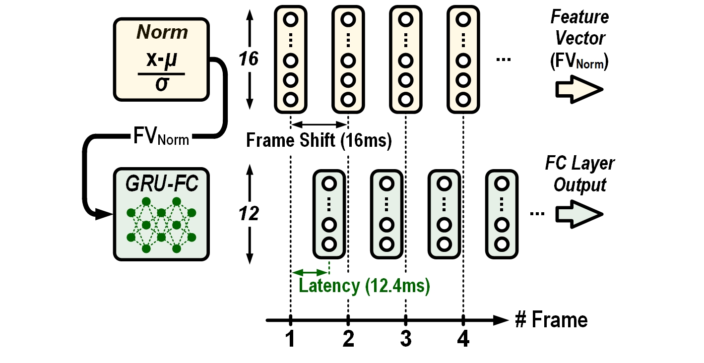
In the digital back-end, the \pdftooltipPFMPulse-Frequency Modulation signals are fed into a digital differentiator (). Here, the signal path from the \pdftooltipSROSwitched-Ring-Oscillator to the digital differentiator builds a first-order Time-to-Digital Converter (TDC) [18] which corresponds to the quantizer in our software model. The output of the digital differentiator is further processed through subsequent stages including a decimation filter which performs the averaging and subsampling operation in our software model. It also includes an offset subtractor () which removes the free-running frequency component of the \pdftooltipSROSwitched-Ring-Oscillator, a per-channel gain calibrator () which corrects the inter-channel gain mismatch, a logarithmic Look-Up Table (LUT), and an input normalizer. Both and shown in Fig. 3 are respectively the mean and the standard deviation of the output of logarithmic \pdftooltipLUTLook-Up Table ( in Fig. 3) from our chip with the \pdftooltipGSCDGoogle Speech Command Dataset training set. With the normalizer, is subtracted from the and the resulting subtracted output is multiplied by a value . The resulting output of the is a 16-channel signed 14-bit \pdftooltipFVFeature Vector which is generated every 16 ms of frame shift as shown in Fig. 4. For each \pdftooltipFVFeature Vector, a 2-layer \pdftooltipGRUGated Recurrent Unit \pdftooltipRNNRecurrent Neural Network and 1-layer \pdftooltipFCFully Connected digital accelerator outputs the most probable keyword over 12 classes with a 12.4 ms latency (see Fig. 4).
III-A Voltage-to-Time Converter
Previous \pdftooltipVADVoice Activity Detection and \pdftooltipKWSKeyword Spotting ICs have used mainly a differential output microphone interface [2, 8, 9]. However, commercial off-the-shelf differential output Micro-Electromechanical Systems (MEMS) microphones typically consume 100 W. To realize a system-level low-power audio \pdftooltipIoTInternet of Things device, a low-power \pdftooltipSESingle-Ended-interface \pdftooltipMEMSMicro-Electromechanical Systems microphone is preferred because it consumes as little as 10 W (e.g., InvenSense ICS-40310 [19]). But this approach makes it difficult to obtain good linearity because \pdftooltipSESingle-Ended signals do not reject even-order harmonics. In general, a linear \pdftooltipFExFeature Extractor is preferred as it makes training the back-end \pdftooltipDNNDeep Neural Network classifier easier and enhances the spectral purity of an audio signal with minimal harmonics and intermodulation distortions. Particularly, the design of a \pdftooltipSESingle-Ended-input ring-oscillator-based \pdftooltipVTCVoltage-to-Time Converter circuit becomes even more difficult because \pdftooltipVCOsVoltage-Controlled Oscillator exhibit poor linearity compared to a conventional voltage-domain Operational Transconductance Amplifier (OTA).
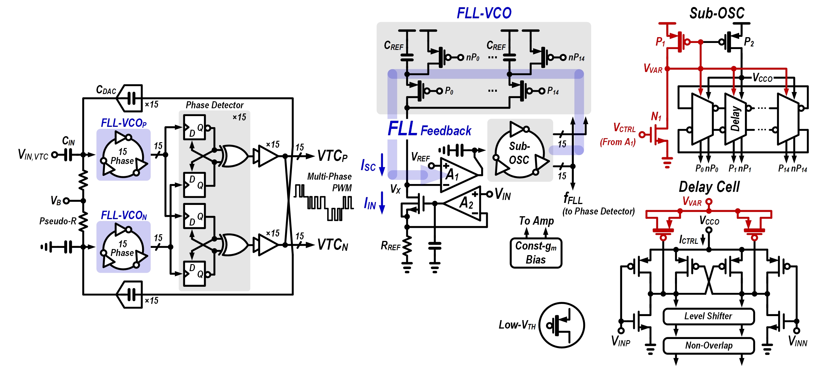
In this work, we propose to use a nested analog \pdftooltipFLLFrequency-Locked Loop around the ring-\pdftooltipVCOVoltage-Controlled Oscillator to enhance the linearity of the \pdftooltipVTCVoltage-to-Time Converter. Fig. 5 shows the architecture and transistor-level schematic of the \pdftooltipFLLFrequency-Locked Loop-based \pdftooltipVTCVoltage-to-Time Converter. The fundamental design principle is adopted from the ring-oscillator-based Low-Pass Filter (LPF) presented in [10], however capacitive coupling is used with to isolate the DC bias of the \pdftooltipVTCVoltage-to-Time Converter from the microphone. Therefore, its core operation is similar to the capacitively-coupled voltage amplifier [20], but the \pdftooltipVTCVoltage-to-Time Converter circuit converts the input voltage into the multi-phase \pdftooltipPWMPulse-Width Modulation output instead of voltage. A pseudo-differential architecture is implemented using a dual-\pdftooltipVCOVoltage-Controlled Oscillator structure along with the phase detector [10]. One input port of the \pdftooltipVTCVoltage-to-Time Converter is connected to the \pdftooltipSESingle-Ended microphone and the other input port is tied to ground. The 15-array phase detector receives a 15-phase frequency-modulated signal out of the \pdftooltipVCOsVoltage-Controlled Oscillator and generates a 15-phase \pdftooltipPWMPulse-Width Modulation output which represents the phase difference of the \pdftooltipVCOsVoltage-Controlled Oscillator. Note that exploiting the multi-phase \pdftooltipPWMPulse-Width Modulation scheme pushes spurious \pdftooltipPWMPulse-Width Modulation tones to higher frequency range without necessitating a higher running frequency of the \pdftooltipVCOVoltage-Controlled Oscillator [10]. The outputs of the phase detector are buffered with two inverters and used to close the feedback loop through a 15-array thermometer-coded capacitive Digital-to-Analog Converter (DAC). Since the input node of the \pdftooltipVCOVoltage-Controlled Oscillator acts as a virtual-ground, the generated multi-phase \pdftooltipPWMPulse-Width Modulation signal becomes a time-domain approximated input voltage where the amplitude is encoded into the duty-cycle of \pdftooltipPWMPulse-Width Modulation. A variation-tolerant pseudo-resistor [21] with a voltage reference sets the common-mode DC bias voltage of the \pdftooltipVCOsVoltage-Controlled Oscillator.
The \pdftooltipFLLFrequency-Locked Loop-based \pdftooltipVCOVoltage-Controlled Oscillator includes a single-branch current comparator [22] to operate the analog \pdftooltipFLLFrequency-Locked Loop. As shown in the schematic diagram of the \pdftooltipFLLFrequency-Locked Loop-\pdftooltipVCOVoltage-Controlled Oscillator in Fig. 5, an input current generator drives the input voltage to to generate a low-side current signal where amplifier is designed to have a 34 dB gain. A high-side current flows through a 15-phase switched-capacitor operation. Here, the multi-phase nature of a ring-oscillator is fully utilized to apply the multi-phase interleaving technique at the node to minimize the voltage ripple caused by the switched-capacitor operation [22]. The low- devices are used to facilitate 0.5 V low-supply operation for the implementation of the switched-capacitor circuit. The \pdftooltipFLLFrequency-Locked Loop feedback formed through the amplifier with a 27 dB gain, sub-\pdftooltipOSCOscillator, and switched-capacitor circuit ensures that equals the reference voltage while also ensuring equals . As a result, the output frequency of the \pdftooltipFLLFrequency-Locked Loop-based \pdftooltipVCOVoltage-Controlled Oscillator is set as in (1).
| (1) | ||||
| (2) |
Since is represented by the input voltage and reference parameters such as , , and , it leads to a \pdftooltipFLLFrequency-Locked Loop-aided linearization of the \pdftooltipVCOVoltage-Controlled Oscillator as derived in (2), where corresponds to the voltage-to-frequency tuning gain. This is because the value of passive elements (, , and ) has no dependency on the input signal amplitude ().
The 3 dB bandwidth of the \pdftooltipVTCVoltage-to-Time Converter circuit is given as below, which is similar to the equation of resistive-input and current-feedback ring-oscillator-based filter [10]
| (3) | |||
| (4) |
where is the gain of phase detector and is the feedback factor (time-to-voltage). We designed to be 17 kHz when the nested \pdftooltipFLLFrequency-Locked Loop feedback has a 158 kHz gain-bandwidth product which contributes as a non-dominant pole to the overall negative feedback loop of the \pdftooltipVTCVoltage-to-Time Converter circuit. As shown in Fig. 7, the stability of the \pdftooltipVTCVoltage-to-Time Converter is verified with a transient simulation.
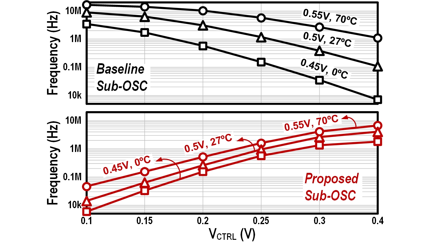
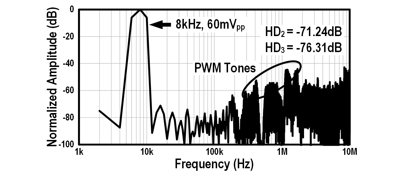
To allow 0.5 V low-supply operation for the sub-\pdftooltipOSCOscillator, a varactor-controlled supply-temperature compensator is proposed. This is achieved by sizing the diode-connected transistor so that becomes proportional-to-absolute-temperature (PTAT) [23]. Therefore, the capacitance of MOS-varactors in the delay cells [24] adaptively stabilizes the temperature drift of the ring-oscillator frequency. For example, if the temperature increases, then also increases, therefore the MOS-varactors are further turned on. This effect negates the frequency increase of the ring-oscillator with temperature increase. Low- MOS capacitors are used to further enhance the varactor effect. In addition, instead of configuring the sub-\pdftooltipOSCOscillator as controlled by the gate voltage of only, the path is added to reduce sensitivity based on the fact that is less sensitive to than . The simulation results in Fig. 6 show that with the proposed techniques, the supply-temperature variation of the sub-\pdftooltipOSCOscillator is reduced by 19.98 in the worst case. Note that the baseline sub-\pdftooltipOSCOscillator refers to the \pdftooltipOSCOscillator circuit assuming that the added compensation circuits (marked as red color in Fig. 5) are removed. In this case, is connected to the gate of the transistor and therefore the frequency tuning curve of sub-\pdftooltipOSCOscillator becomes decreasing function as increases. Fig. 7 shows the post-layout simulation result of the \pdftooltipVTCVoltage-to-Time Converter. The plotted graph represents the multi-phase \pdftooltipPWMPulse-Width Modulation signal of \pdftooltipVTCVoltage-to-Time Converter output (). The designed \pdftooltipVTCVoltage-to-Time Converter converts a voltage-domain input into a time-domain \pdftooltipPWMPulse-Width Modulation output while ensuring -70 dB distortion for dominant harmonics (second and third) even with a \pdftooltipSESingle-Ended input. The \pdftooltipPWMPulse-Width Modulation tones at higher frequencies are filtered out at the following \pdftooltipBPFBand-Pass Filter stage.
III-B Time-Domain Band-Pass Filter
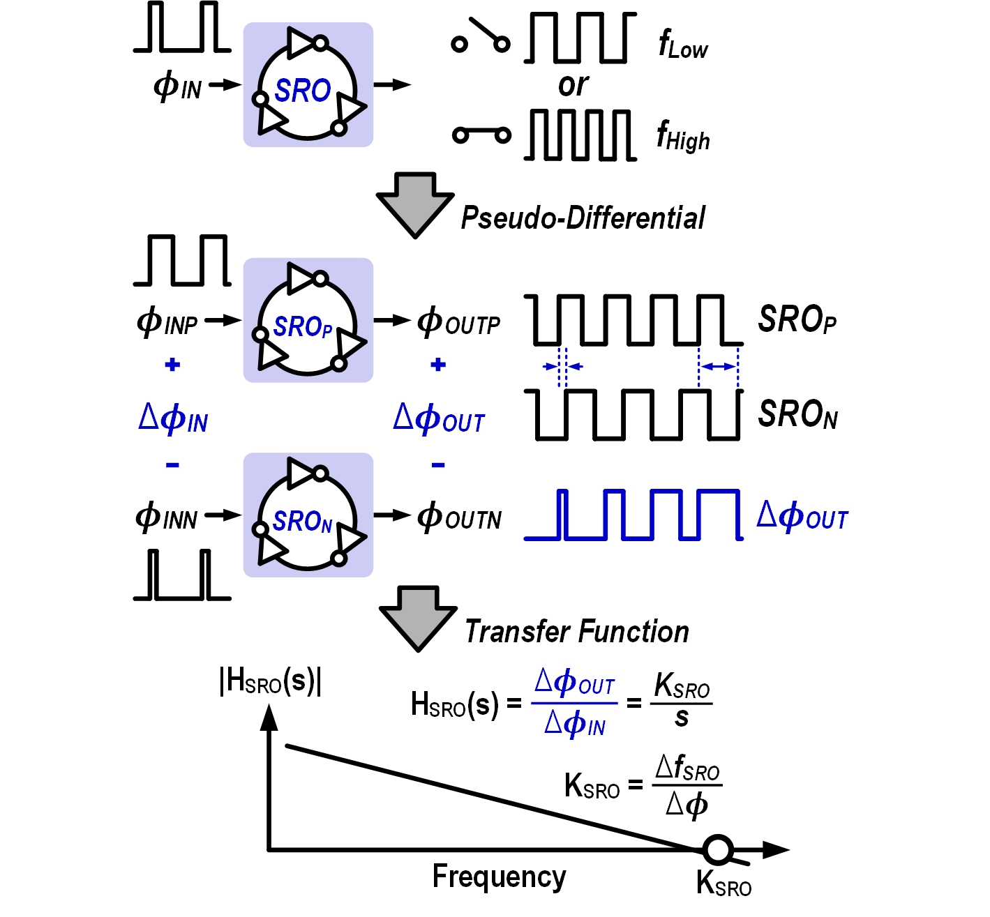
Fig. 8 shows a conceptual diagram of using the switched-ring-oscillator (SRO) [18] as an ideal -to- integrator. The \pdftooltipSROSwitched-Ring-Oscillator switches its running frequency between and according to the incoming input \pdftooltipPWMPulse-Width Modulation signal. The averaged value of \pdftooltipSROSwitched-Ring-Oscillator frequency is proportional to the duty-cycle of the input \pdftooltipPWMPulse-Width Modulation signal. If the input \pdftooltipPWMPulse-Width Modulation signal is configured as a multi-phase format, the possible number of running frequencies also increases. When the dual-\pdftooltipSROSwitched-Ring-Oscillator is implemented in a pseudo-differential manner, the output phase difference becomes an accumulated (or integrated) input phase difference over time. Specifically, this integral procedure flows as following. Input Phase SRO Frequency SRO Phase (+Integral) Output Phase. The phase mathematically represents an integral amount of the frequency within an oscillator. This time-domain accumulation process allows an integral of the signal without boundary as long as the \pdftooltipSROSwitched-Ring-Oscillator oscillates, unlike voltage-domain designs that saturate due to headroom. In other words, it shows an infinite DC gain and acts as a true lossless integrator regardless of the intrinsic gain of transistor or supply voltage level [10]. As shown in the lowermost description of Fig. 8, the -to- transfer function is described by where is the switching gain of a \pdftooltipSROSwitched-Ring-Oscillator.
Fig. 9 shows a conceptual diagram for the implementation of a time-domain -to- \pdftooltipBPFBand-Pass Filter. It adopts the two-integrator-loop Tow-Thomas biquad topology [25, 26] using \pdftooltipSROSwitched-Ring-Oscillator as a lossless integrator (). The Phase Detector (PD) extracts the phase difference between two input signals and outputs the phase difference in a \pdftooltipPWMPulse-Width Modulation signal. The output of \pdftooltipPDPhase Detector is used to close the feedback loops where the inner feedback loop ensures the desired factor and the outer feedback loop generates the high-pass shape of the \pdftooltipBPFBand-Pass Filter. Overall, the time-domain \pdftooltipBPFBand-Pass Filter receives the \pdftooltipPWMPulse-Width Modulation input and generates the \pdftooltipPWMPulse-Width Modulation output. Note that an external clock is fed to the \pdftooltipPDPhase Detector in Fig. 9 since it is represented as a simplified half-circuit diagram. If the two \pdftooltipBPFsBand-Pass Filter are placed in parallel to work as a pseudo-differential configuration as shown in Fig. 8, the external clock is no longer needed and the \pdftooltipBPFBand-Pass Filter operates in a fully asynchronous way. The same consideration for a pseudo-differential topology also applies to the \pdftooltipVTCVoltage-to-Time Converter design as described in Section III-A.
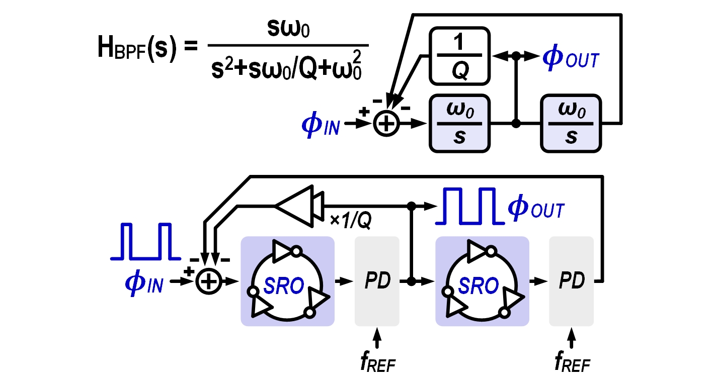
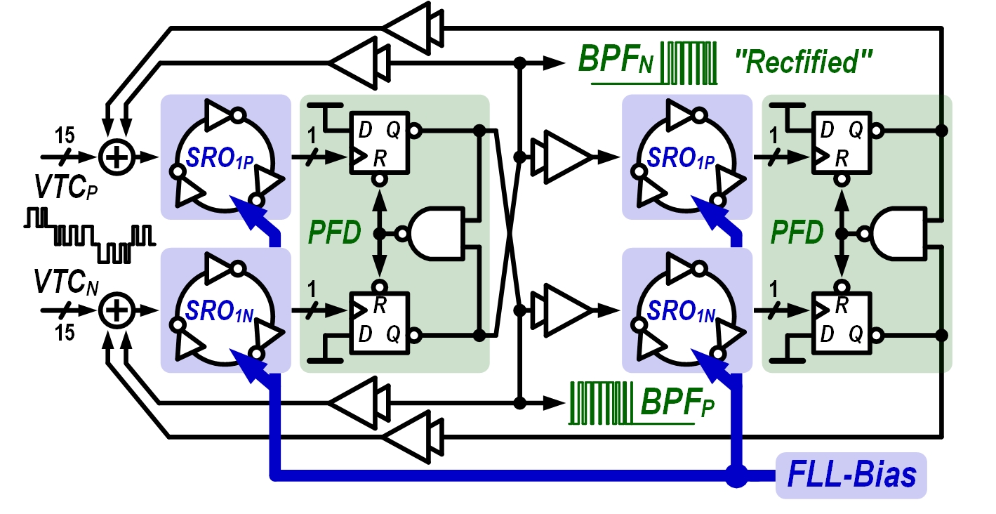

Fig. 10 shows the block diagram of the proposed time-domain \pdftooltipBPFBand-Pass Filter. It receives the multi-phase \pdftooltipPWMPulse-Width Modulation output of the \pdftooltipVTCVoltage-to-Time Converter as an input signal and does not require an external clock. It incorporates four \pdftooltipSROsSwitched-Ring-Oscillator and two Phase Frequency Detector (PFD). The outputs of the \pdftooltipBPFBand-Pass Filter are two single-phase \pdftooltipPWMPulse-Width Modulation signals. The two \pdftooltipPFDsPhase Frequency Detector implemented in the \pdftooltipBPFBand-Pass Filter offers an inherent rectification function in time-domain, which will be discussed in Section III-C. A local \pdftooltipFLLFrequency-Locked Loop-based bias generator provides the required bias voltage which are shared over the four \pdftooltipSROsSwitched-Ring-Oscillator. This bias voltage is different over 16-channel \pdftooltipBPFBand-Pass Filter bank to set different center frequencies. Note that the outputs of first \pdftooltipPFDPhase Frequency Detector are crossed and connected to the \pdftooltipSROsSwitched-Ring-Oscillator with opposite polarities, to realize a subtraction function.
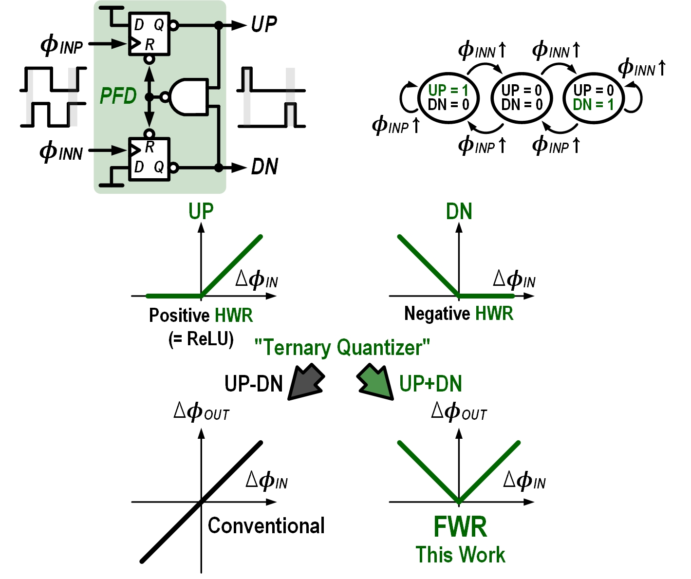
Fig. 11 shows a schematic of the \pdftooltipFLLFrequency-Locked Loop-based bias generator and \pdftooltipSROsSwitched-Ring-Oscillator used in our \pdftooltipBPFBand-Pass Filter design. The \pdftooltipSROSwitched-Ring-Oscillator receives time-domain \pdftooltipPWMPulse-Width Modulation signals as input, such as \pdftooltipVTCVoltage-to-Time Converter and \pdftooltipPFDPhase Frequency Detector. All the \pdftooltipPWMPulse-Width Modulation signals are summed at the internal node of the \pdftooltipSROSwitched-Ring-Oscillator and these signals drive the buffers which act as an array of current-mode \pdftooltipDACsDigital-to-Analog Converter. Therefore, the output frequency of \pdftooltipSROSwitched-Ring-Oscillator is proportional to the sum of incoming \pdftooltipPWMPulse-Width Modulation signals. To realize different switching gains of \pdftooltipPWMPulse-Width Modulation inputs, switching transistors are differently sized. The unit current for current-\pdftooltipDACDigital-to-Analog Converter operation is provided by a local \pdftooltipFLLFrequency-Locked Loop circuit. The \pdftooltipFLLFrequency-Locked Loop acts as a bias generator for realization of per-channel center frequency designs in \pdftooltipBPFsBand-Pass Filter, using a replica biasing scheme. As shown in Fig. 11, the bias voltage is generated from a diode-connected pFET in the FLL-bias circuit. Therefore, the current-\pdftooltipDACDigital-to-Analog Converter in \pdftooltipSROSwitched-Ring-Oscillator1-2 operates as a current mirror when is shared over the four \pdftooltipSROsSwitched-Ring-Oscillator from the \pdftooltipFLLFrequency-Locked Loop-bias circuit. This means that the switching gain of each \pdftooltipPWMPulse-Width Modulation input signal is determined by and the sizing ratio of the current-mode \pdftooltipDACDigital-to-Analog Converter. For example, the switching gain of \pdftooltipVTCVoltage-to-Time Converter-port is and the switching gain of \pdftooltipPFDPhase Frequency Detector2-port fed into the \pdftooltipSROSwitched-Ring-Oscillator2 is . Note that we adopt the same circuit structure from the sub-\pdftooltipOSCOscillator circuit in Section III-A which allows the \pdftooltipBPFBand-Pass Filter to work at 0.5 V low-supply voltage. As discussed in (1), the locking frequency of the \pdftooltipFLLFrequency-Locked Loop circuit is proportional to . To cover the target range of \pdftooltipBPFBand-Pass Filter center frequencies ranging from 100 Hz to 8 kHz in our design, a coarse-fine approach is used. The output of \pdftooltipSROSwitched-Ring-Oscillator is divided coarsely by times using D Flip-Flop (D-FF) and the of \pdftooltipFLLFrequency-Locked Loop circuit is fine controlled through proper sizing. The complete transfer function of the proposed time-domain \pdftooltipBPFBand-Pass Filter is given in (5). Its center frequency and -factor are given in (6) where the -factor is designed as 2 for each \pdftooltipBPFBand-Pass Filter channel by proper sizing of the switching transistors in the \pdftooltipSROsSwitched-Ring-Oscillator. The stability of the proposed second-order time-domain \pdftooltipBPFBand-Pass Filter is verified with a transient simulation.
| (5) |
| (6) |
III-C Time-Domain Rectifier
Fig. 12 shows the schematic of \pdftooltipFWRFull-Wave Rectifier. The proposed time-domain \pdftooltipFWRFull-Wave Rectifier is based on a simple \pdftooltipPFDPhase Frequency Detector circuit consisting of only two \pdftooltipD-FFsD Flip-Flop and one NAND gate. Compared to the prior voltage-domain design [8] that required several scaling-unfriendly \pdftooltipOTAsOperational Transconductance Amplifier, references, and passive elements, this work offers an alternative solution that is fully compatible with standard logic gates. Fig. 12 shows a state diagram and an input-output characteristic of the \pdftooltipPFDPhase Frequency Detector. The \pdftooltipPFDPhase Frequency Detector circuit extracts the input phase difference , but at the same time asynchronously quantizes the phase difference using a ternary code with UP and down (DN) signals. As shown in the state diagram, there are three states that are activated by the rising edges of incoming \pdftooltipPWMPulse-Width Modulation signals (, ). When both UP and DN signals are high, the NAND gate resets two \pdftooltipD-FFsD Flip-Flop immediately, thereby making itself as a ternary quantizer. Since the state of \pdftooltipPFDPhase Frequency Detector stays the same unless a new rising edge arrives, the UP and DN signal represents a positively and negatively Half-Wave Rectified (HWR) phase difference , respectively. Interestingly, the UP signal has the same form as the Rectified Linear Unit (ReLU) activation function widely used in modern \pdftooltipDNNsDeep Neural Network. In conventional usage of such signals like in Phase-Locked Loop (PLL) designs, they are subtracted to derive a linearized phase difference extractor. However, if we add them, a time-domain \pdftooltipFWRFull-Wave Rectifier can be implemented. The \pdftooltipPFDPhase Frequency Detector-based \pdftooltipFWRFull-Wave Rectifier benefits from its fully time-domain nature, that is, it does not exhibit a headroom-related saturation, assuming that the input signal swing () is within range. As shown in Fig. 10, the proposed time-domain \pdftooltipFWRFull-Wave Rectifier is seamlessly integrated within the time-domain \pdftooltipBPFBand-Pass Filter circuit and thus the \pdftooltipBPFBand-Pass Filter provides an inherent rectification function. The rectified \pdftooltipPWMPulse-Width Modulation signals () are summed at the subsequent \pdftooltipPFMPulse-Frequency Modulation stage as described in Fig. 13.

III-D Pulse-Frequency Encoder and Time-to-Digital Converter
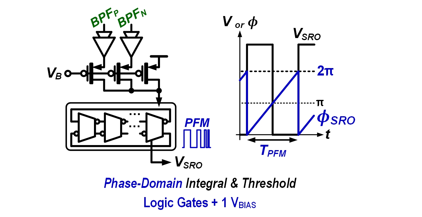
The analog \pdftooltipFExFeature Extractor designs presented in [8, 9] used an Integrate-and-Fire (IAF) circuit which was originally proposed in [27]. The circuit converts an input current into a rate-encoded spiking \pdftooltipPFMPulse-Frequency Modulation signal and its spiking frequency is proportional to the input current magnitude. The \pdftooltipIAFIntegrate-and-Fire circuit can be interpreted as a Current-Controlled Oscillator (CCO) where the core oscillator topology is equivalent to a relaxation oscillator [28]. However, the \pdftooltipIAFIntegrate-and-Fire circuit is scaling-unfriendly because of its voltage-domain integral operation and voltage-domain static amplifier as discussed in Section I. In this work, we propose to use the \pdftooltipSROSwitched-Ring-Oscillator as a \pdftooltipPFMPulse-Frequency Modulation encoder instead of the \pdftooltipIAFIntegrate-and-Fire circuit. As shown in Fig. 14, the \pdftooltipSROSwitched-Ring-Oscillator exploits an inherent phase-domain threshold and its integral operation occurs in the phase-domain which is free from headroom issue. The proposed \pdftooltipSROSwitched-Ring-Oscillator-based design offers a scaling-friendly implementation using only logic gates and bias generator without a static amplifier or passive components.
In previous designs [8, 9], an asynchronous ripple-carry counter associated with a multi-bit register was used to quantize and sample the input \pdftooltipPFMPulse-Frequency Modulation signal. Interestingly, given the aforementioned interpretation of \pdftooltipIAFIntegrate-and-Fire circuit as an oscillator, the signal flow from an \pdftooltipIAFIntegrate-and-Fire to a counter builds an \pdftooltipVCOVoltage-Controlled Oscillator/\pdftooltipCCOCurrent-Controlled Oscillator-based modulator [29, 18]. However, the design approaches used in [8, 9] had two major problems. First, the ripple-carry counter exhibits metastability-induced data corruption when the sampling occurs at the instant of multibit transition of binary codes. Second, the output digital data from the asynchronous counter, which is modulated, was directly fed to the \pdftooltipDNNDeep Neural Network classifier without filtering of high-pass-shaped quantization noise. Our approach uses arrayed 1-bit XOR differentiators [30] to solve the metastability problem and an oversampling associated with a decimation filter to filter out quantization noise.
Fig. 13 shows the overview of implemented 16-channel \pdftooltipSROSwitched-Ring-Oscillator-based \pdftooltipPFMPulse-Frequency Modulation encoder, XOR differentiator, and subsequent post-processing stages, also with the signal flow domains at the top. The \pdftooltipSROSwitched-Ring-Oscillator receives rectified \pdftooltipPWMPulse-Width Modulation signals from the preceding \pdftooltipBPFBand-Pass Filter stage and converts it into 15-phase \pdftooltipPFMPulse-Frequency Modulation signals. The same design of \pdftooltipFLLFrequency-Locked Loop circuit discussed in Section III-B is reused for biasing of the \pdftooltipSROSwitched-Ring-Oscillator where the generated bias voltage is shared over 16 channels. As the ring-\pdftooltipOSCOscillator output is represented in thermometer-code, the XOR differentiator ensures the worst-case error to be within 1-Least Significant Bit (LSB). In addition, this 1-\pdftooltipLSBLeast Significant Bit error is noise-shaped [31] which can be eliminated through oversampling and decimation filtering. The thermometer-coded output data is aggregated to be represented as binary format and then filtered and decimated through a 1st-order Cascaded Integrator–Comb (CIC) filter. We use 210 decimation size, i.e., , and is used in the post-processing blocks which incorporates a programmable offset () subtractor to remove the DC offset due to a free-running component of the \pdftooltipSROSwitched-Ring-Oscillator-based \pdftooltipPFMPulse-Frequency Modulation encoder. A programmable per-channel gain calibrator () is used to correct inter-channel gain deviations caused by mismatch of SROs in the PFM encoder. A logarithmic compression using a LUT and a programmable input normalizer helps to increase the classification accuracy of the following \pdftooltipGRUGated Recurrent Unit-\pdftooltipFCFully Connected neural network. The post-processing stage is clocked at 61 Hz and thus its power dissipation is negligible.
III-E Recurrent Neural Network Accelerator
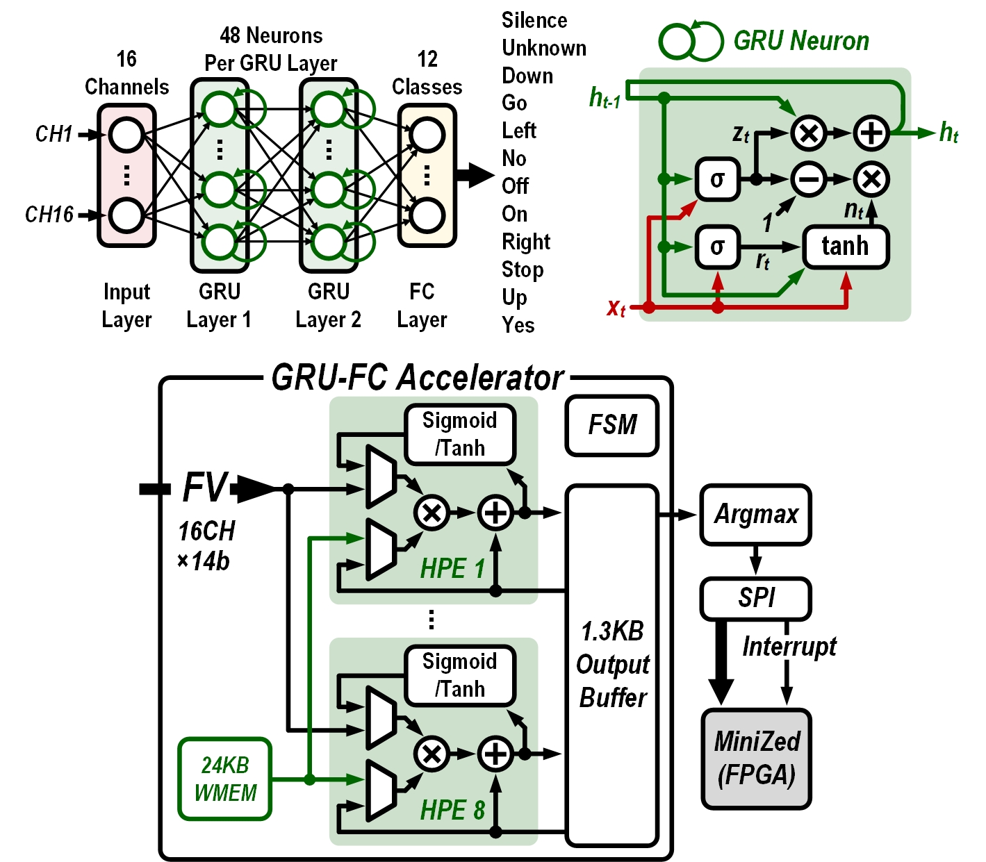
Fig. 15 shows the architectures of the \pdftooltipGRUGated Recurrent Unit-\pdftooltipFCFully Connected network and accelerator. The network has two \pdftooltipGRUGated Recurrent Unit layers with 48 units per layer and a final \pdftooltipFCFully Connected layer that generates the confidence scores of the 12 classes. The network model size is entirely buffered within the 24 KB Weight Memory (WMEM). The accelerator computes the \pdftooltipKWSKeyword Spotting classifier network and its input comes from the normalizer shown in Fig. 13. The \pdftooltipWMEMWeight Memory block is implemented by on-chip Static Random Access Memory (SRAM) compiled based on the foundry-provided 6-transistor (6T) bit-cell. The classifier weights are loaded into \pdftooltipWMEMWeight Memory over the SPI interface. The accelerator has 8 Heterogeneous Processing Elements (HPEs) controlled by a Finite-State Machine (FSM). Each HPE has a 14-bit multiplier, a 24-bit accumulator, and a LUT-based Sigmoid/Tanh unit. Partial sums of the multiply-accumulate operations and outputs are stored in a shared 1.3 KB \pdftooltipSRAMStatic Random Access Memory output buffer. Multiplexers before each multiplier operand select inputs from the normalizer, the Sigmoid/Tanh unit, the \pdftooltipWMEMWeight Memory, and the output buffer to compute element-wise vector multiplication/addition and hyperbolic functions in the \pdftooltipGRUGated Recurrent Unit \pdftooltipRNNRecurrent Neural Network. The high device library is used for logic synthesis to reduce leakage current. Output scores of the classifier are fed to the argmax decoder, which outputs the class with the highest score. The classification result is transmitted over the SPI interface with an interrupt flag to the external host, which is a MiniZed board with a Xilinx Zynq-7007S SoC.
III-F Network Training
Dataset preparation
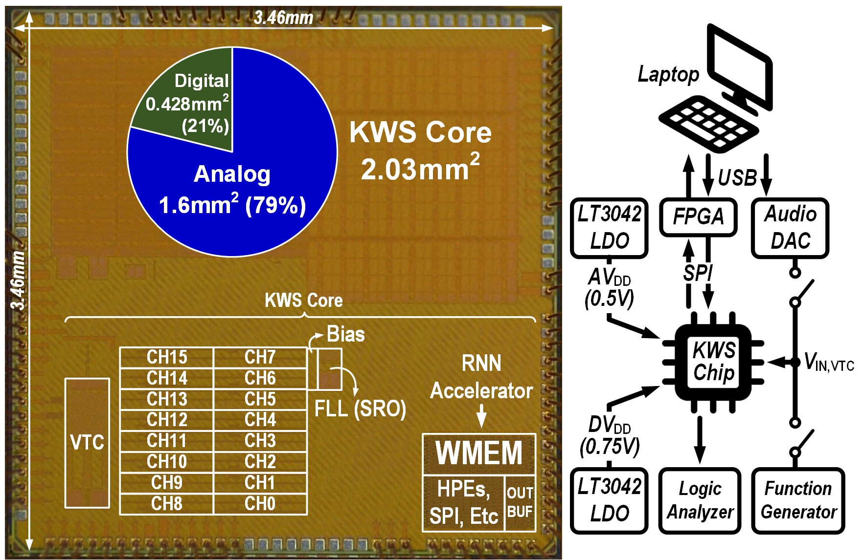
Our \pdftooltipGSCDGoogle Speech Command Dataset training set is composed of 38,463 samples. The number of samples in the “Silence” class is 4,044 which are randomly sampled from the background noise tracks in the dataset. The “Unknown” class also has 4,044 samples which are randomly chosen words outside the target 12 classes. As for the test set, we used the standard \pdftooltipGSCDGoogle Speech Command Dataset test set111http://download.tensorflow.org/data/speech_commands_test_set_v0.02.tar.gz which has roughly equal number of samples (around 400) among the 12 target classes. Thus, the ratio between training and test set is around 8:1. As shown in the measurement setup of Fig. 16, the samples from our entire training and test set were played from a laptop to through a USB sound card \pdftooltipDACDigital-to-Analog Converter (Sound Blaster E1). We normalized the \pdftooltipGSCDGoogle Speech Command Dataset samples with the mean and standard deviation of the entire samples such that the amplitude of is set to 250 mVPP. The corresponding from all samples were recorded. They were then corrected for the DC offset () and the inter-channel gain deviation (). After applying the logarithmic compression, we then normalize the with the mean () and standard deviation () of the recorded feature vectors from the entire \pdftooltipGSCDGoogle Speech Command Dataset training set. This resulting vector called (see Fig. 3) are then presented as inputs to the \pdftooltipGRUGated Recurrent Unit-\pdftooltipFCFully Connected classifier during training. The same and are applied to of the test set to generate the corresponding for \pdftooltipKWSKeyword Spotting evaluation.
Training schedule
The network is built in the PyTorch 1.8 framework and trained for 200 epochs using the AdamW optimizer [32] with an initial learning rate of 1e-3 and 0.01 weight decay. The ReduceLROnPlateau learning rate scheduler is used with a decay factor of 0.8 and patience of 3 epochs. The lowest learning rate is 5e-4. Using quantization-aware training, the activations and weights are quantized to 14-bits and 8-bits respectively.
IV Measurement Results
Fig. 16 shows the \pdftooltipKWSKeyword Spotting IC, which is fabricated in TSMC 65 nm CMOS LP process with an active area of 2.03mm2 for the \pdftooltipKWSKeyword Spotting core. The area occupied by the analog and digital circuits is 1.6mm2 (79%) and 0.428mm2 (21%) respectively in the \pdftooltipKWSKeyword Spotting core. The \pdftooltipGRUGated Recurrent Unit-\pdftooltipFCFully Connected neural network accelerator and the associated peripherals in the digital circuits are synthesized from a standard auto place-and-route (P&R) flow.
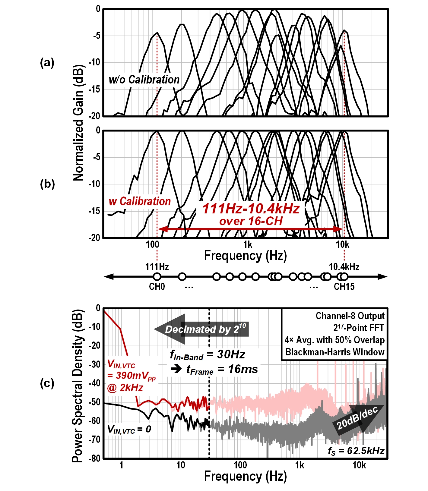
Fig. 17(a) and (b) show the measured frequency response of the 16-channel \pdftooltipFExFeature Extractor with and without per-channel gain calibration. In this case, was connected to a function generator. The center frequencies of the 16 \pdftooltipBPFBand-Pass Filter channels range from 111 Hz to 10.4 kHz. The center frequencies are distributed according to the Mel scale therefore low-frequency (1 kHz) channels are spaced further apart than high-frequency channels. As shown in Fig. 17(a), the measured gain curve before the calibration shows the inter-channel gain deviations which are caused by systematic mismatches from the \pdftooltipSROSwitched-Ring-Oscillator-based \pdftooltipPFMPulse-Frequency Modulation encoder. The main cause of gain deviation is the voltage bias ( in Fig. 11) which is generated from a single \pdftooltipFLLFrequency-Locked Loop circuit and it is shared over the 16-channel \pdftooltipSROSwitched-Ring-Oscillator as depicted as ‘\pdftooltipFLLFrequency-Locked Loop (\pdftooltipSROSwitched-Ring-Oscillator)’ in the chip photograph. We expect this systematic mismatch due to distribution of the voltage bias can be improved with a better layout floorplan, for example with a centralized placement of the bias circuits while the random mismatch can be improved with larger sizing of the biasing transistors.
Fig. 17(c) shows the measured output spectrum of channel 8 for two different input conditions of the \pdftooltipVTCVoltage-to-Time Converter; the black curve is obtained with a zero input condition while the red curve is obtained with a 2 kHz sinusoidal input of 390 mVPP. Here, the amplitude of the input to the \pdftooltipVTCVoltage-to-Time Converter circuit was assumed to be sufficiently large, and our future work will include an additional ultra-low-power pre-amplifier [33] before the \pdftooltipVTCVoltage-to-Time Converter circuit. The oversampling clock frequency that is fed into the XOR differentiator is 62.5 kHz. It is clearly seen that the output spectrum has a first-order noise-shaping property with a 20 dB/dec slope for both input conditions. After the feature data is decimated by 210, the in-band frequency is limited as 30 Hz which is translated into a 16 ms frame shift or 61 frame/s throughput, and so the 16-channel \pdftooltipFVFeature Vector is generated every 16 ms. The integrated in-band noise with zero input is calculated as 248 VRMS, which is dominated by noise. When the input amplitude is increased to 390 mVPP, the in-band noise is dominated by thermal noise. We believe that the noise increase is caused by a higher running frequency of the \pdftooltipSROSwitched-Ring-Oscillator, since the phase noise of ring oscillators increases with operating frequency [34].
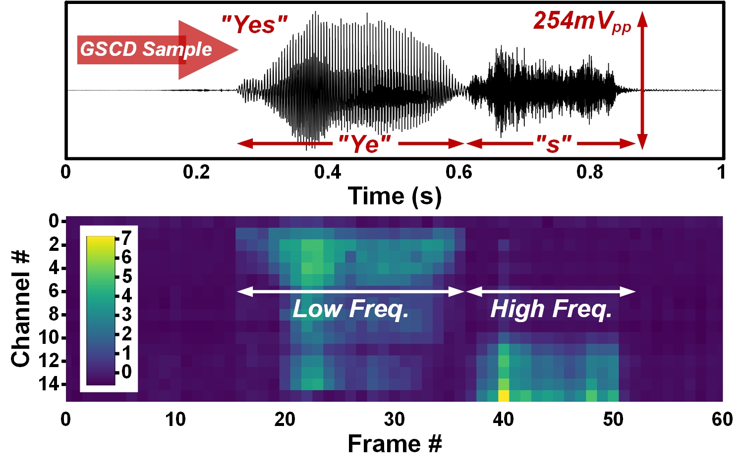
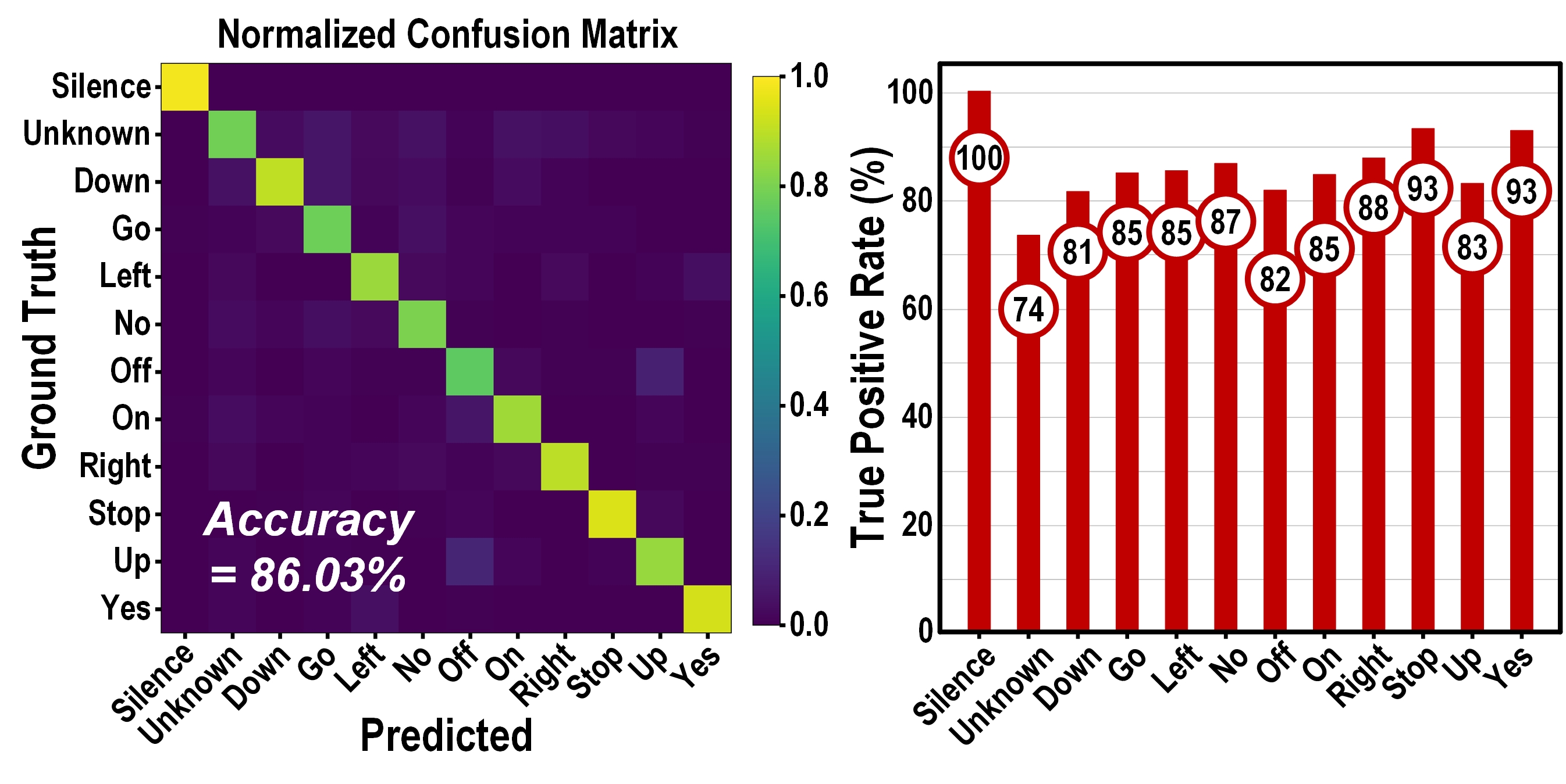
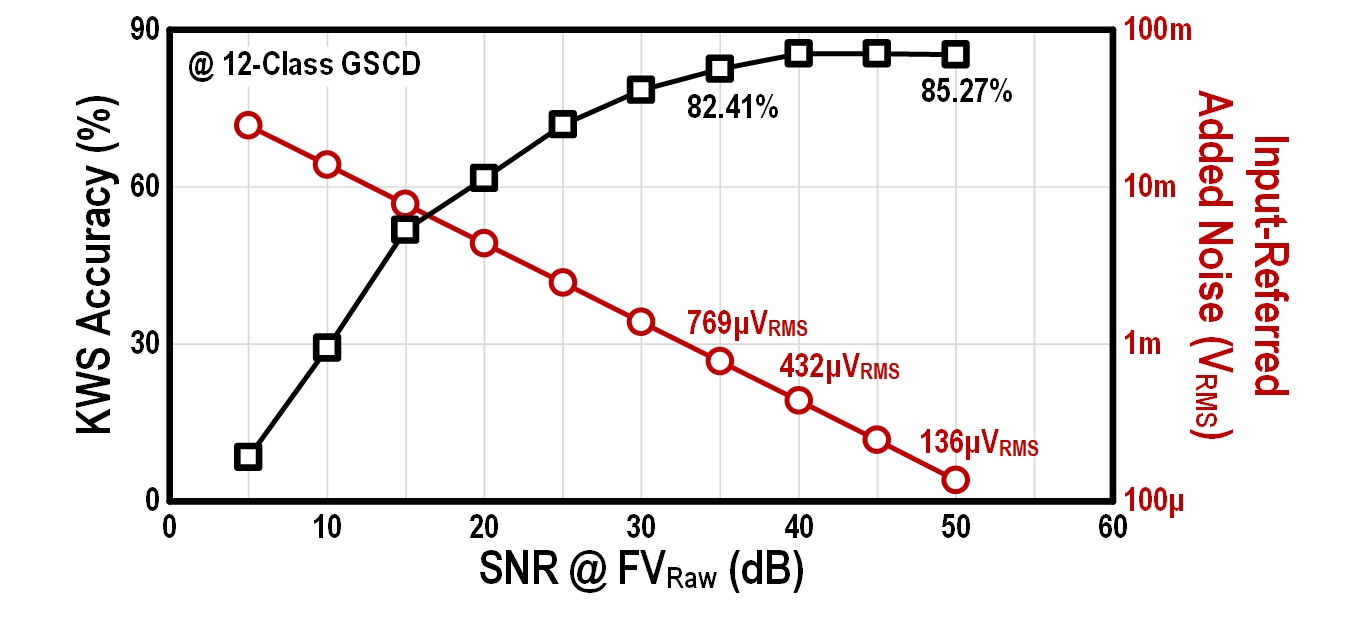
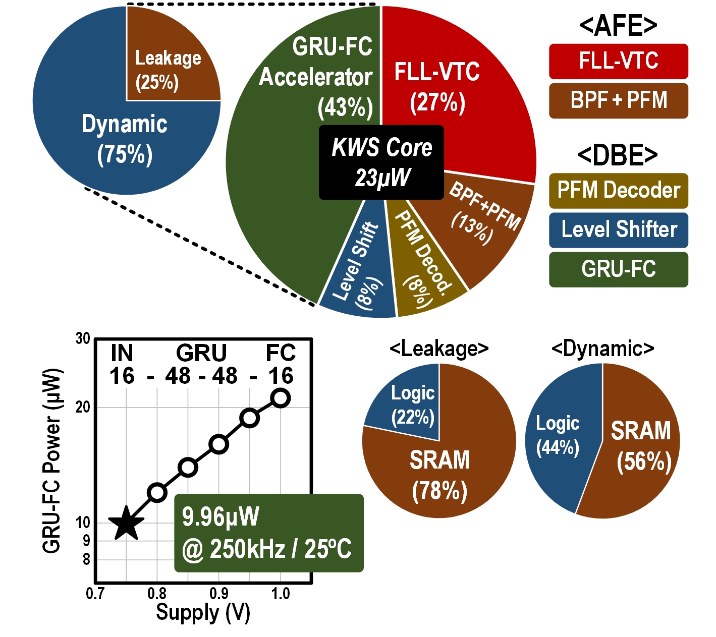
Fig. 18 shows the measured audio response of the \pdftooltipFExFeature Extractor. A 254 mVPP “Yes” keyword sample from \pdftooltipGSCDGoogle Speech Command Dataset is selected and applied to the \pdftooltipVTCVoltage-to-Time Converter while measuring the \pdftooltipFExFeature Extractor output. The magnitudes of \pdftooltipFVFeature Vector in this figure are normalized by subtracting DC offset and dividing by the standard deviation of the sample clip, for better visualization. It is clearly seen that the 16-channel \pdftooltipFVFeature Vector has higher response at low frequencies for the “Ye” sound, and at higher frequencies for the “s” sound.
Fig. 19 shows the measured \pdftooltipKWSKeyword Spotting accuracy of the prototype chip obtained using the full 12-class verification flow of the \pdftooltipGSCDGoogle Speech Command Datasetv2 [35]. The 12 classes include “Silence”, “Unknown”, and 10 target keywords. As shown in the measurement setup in Fig. 16, the generated \pdftooltipFVsFeature Vector ( in Fig. 3) from our time-domain \pdftooltipFExFeature Extractor are recorded using the \pdftooltipGSCDGoogle Speech Command Dataset training set that is fed to the \pdftooltipVTCVoltage-to-Time Converter of our chip ( in Fig. 16), to train the classifier network. The 16 ms frame window and 16 ms frame shift (stride) are used for recording, so there is no overlap between two consecutive frames. The detected class is the most active output at the end of the \pdftooltipGSCDGoogle Speech Command Dataset sample. The prototype \pdftooltipKWSKeyword Spotting IC achieves an overall 86.03% accuracy with the \pdftooltipGSCDGoogle Speech Command Dataset test set. The measured true positive rates show that “Silence” is the easiest class with 100% accuracy and the classifier performed the best on two keywords, “Stop” and “Yes,” with 93% accuracy. The most challenging class is “Unknown” class since it includes 25 non-target keywords such as “Happy” and “Dog,” which requires the classifier to train more parameters with larger model capacity to improve the accuracy. We expect that the detection accuracy of “Unknown” and thus the overall accuracy on this \pdftooltipKWSKeyword Spotting dataset will improve with a larger network model, but at the expense of additional power consumption and silicon area. The state-of-the-art accuracy on \pdftooltipGSCDGoogle Speech Command Dataset using \pdftooltipGRUGated Recurrent Unit-\pdftooltipRNNsRecurrent Neural Network is 94.2% [36] with a network which has 499 KB parameters and running on a Cortex-M7 microcontroller. This network size would require 21 more on-chip memory leading to higher power consumption and chip area.
| Analog FEx |
|
|
|
|
This Work | ||||||||||
|---|---|---|---|---|---|---|---|---|---|---|---|---|---|---|---|
| Process (nm) | 180 | 90 | 180 | 180 | 65 | ||||||||||
| Area/Ch. (mm2) | 0.26 | 0.13 | 0.1 | - | 0.1 | ||||||||||
| Architecture | gmC-\pdftooltipBPFBand-Pass Filter | gmC-\pdftooltipBPFBand-Pass Filter | gmC-\pdftooltipBPFBand-Pass Filter | Mixer | OSC-BPF | ||||||||||
| Number of Ch. | 642 | 16 | 16 | 32A | 16 | ||||||||||
| Freq. Range (Hz) | 8-20k | 75-5k | 100-5k | 75-4k | 111-10.4k | ||||||||||
| Supply (V) | 0.5 | - | 0.6 | 1.4 | 0.5 | ||||||||||
| Power (W) | 55 | 6 | 0.38 | 0.06 | 9.3 | ||||||||||
| Frame Shift (ms) | - | 31.25B | 10 | 512A | 16 | ||||||||||
| Dynamic Range (dB) | 55 | 45 | 40C | 47 | 54.89 | ||||||||||
| FoMS,DR (dB) | - | 82.3 | 91.5 | 91.33 | 93.11 | ||||||||||
| Target Task | General Purpose | VAD | KWS | ||||||||||||
| Building Blocks |
|
|
|
|
|
||||||||||
| Support SE Mic | No | ✓ | No | ✓ | ✓ | ||||||||||
| Parallel FEx | ✓ | ✓ | ✓ | No | ✓ | ||||||||||
| AWith 32-32-16-2 FC neural network BfLPF = 16 Hz | |||||||||||||||
| CMeasured by the firing rate range of the IAF only, excluding output noise of the feature vector | |||||||||||||||
| (7) |
| (8) |
| KWS |
|
|
|
|
|
This Work | |||||||||||||||
| - | Off-Chip ADC | On-Chip ADC | On-Chip Analog FEx | ||||||||||||||||||
| Process (nm) | 28 | 65 | 28 | 65 | 65 | 65 | |||||||||||||||
| Area (mm2) | 1.29A | 4.13A | 0.23A | 1.52 | 2.71B | 2.03 | |||||||||||||||
| SRAM (KB) | 52 | 38 | 2 | 32 | 20 | 27 | |||||||||||||||
| Clock (Hz) | 2.5M | 1G | 40k | 250k | 120k | 250k | |||||||||||||||
| FEx | Digital | - | Digital | Digital | Analog Voltage | Analog Time | |||||||||||||||
| Classifier | CNN | RNN | CNN | RNN | SNN (MLP) | RNN | |||||||||||||||
| KWS Power (W) | 141A | 11000A | 0.51A | 16.1 | 0.205-0.570 | 23 | |||||||||||||||
| Frame Shift (ms) | 10 | 20 | 16 | 16 | 100 | 16 | |||||||||||||||
| Latency (ms) | 10 | 0.04 | 64 | 16 | 100 | 12.4 | |||||||||||||||
| Dataset | TIDIGITS | GSCD | |||||||||||||||||||
|
2 |
|
|
|
|
|
|
||||||||||||||
|
96 | 90.38 |
|
|
90.87 | 90.2 | 86.03 | ||||||||||||||
| Support SE Mic | Off-Chip ADC | No | No | ✓ | |||||||||||||||||
| AExcluding off-chip ADC BIncluding SNN chip [40] CExcluding “Unknown” word detection as a distinct class | |||||||||||||||||||||
| D2 non-keywords (Silience/Unknown) + 10 keywords EAccuracy is reported from 16-bit GSCD samples; the design excludes the 16-bit ADC | |||||||||||||||||||||
Fig. 20 shows the dependence of the \pdftooltipKWSKeyword Spotting classification accuracy on added noise levels to the recorded feature vector (see Fig. 3). We first computed the average power using the recorded (see Section III-F). Then Gaussian noise of different standard deviation values () were added to create different SNR values following the equation below.
| (9) |
The noise is randomly generated for each training epoch and test evaluation. For each \pdftooltipSNRSignal-to-Noise Ratio case, our \pdftooltipGRUGated Recurrent Unit-\pdftooltipFCFully Connected network is retrained using the noisy training set and the noisy test set is used to evaluate the classification accuracy. The proposed \pdftooltipKWSKeyword Spotting IC ensures 1% accuracy drop even for noise levels up to 432 VRMS (input-referred to ), or 40 dB \pdftooltipSNRSignal-to-Noise Ratio.
Fig. 21 shows the power breakdown of the \pdftooltipKWSKeyword Spotting IC. As it is stated in Section I, this paper focuses on the \pdftooltipKWSKeyword Spotting core only therefore the power breakdown in Fig. 21 does not include energy harvester, low-dropout regulator, and voltage reference circuits. The total power consumption of the \pdftooltipKWSKeyword Spotting core is 23 W when it is measured at 25∘C room temperature. The \pdftooltipGRUGated Recurrent Unit-\pdftooltipFCFully Connected neural network accelerator accounts for 43% of the \pdftooltipKWSKeyword Spotting core power. When the 16IN-48H-48H-12C \pdftooltipGRUGated Recurrent Unit-\pdftooltipFCFully Connected network is updated at 250 kHz clock frequency and 0.75 V supply voltage while performing continual inference on random \pdftooltipGSCDGoogle Speech Command Dataset samples with 16 ms frame shift, the accelerator consumes 9.96 W. The accelerator power consumption can be further decomposed into dynamic power (75%) and leakage (or static) power (25%). The leakage power is dominated by the \pdftooltipSRAMStatic Random Access Memory block (78%) while both logic (44%) and \pdftooltipSRAMStatic Random Access Memory (56%) contributed rather evenly to the dynamic power. We expect that leakage power can be reduced with custom memory cells [6].
Table I compares the performance of our time-domain \pdftooltipFExFeature Extractor with the state-of-the-art voice processing analog \pdftooltipFExFeature Extractor [37, 8, 7, 3]. The proposed \pdftooltipFExFeature Extractor circuit is the first that demonstrated ring-oscillator-based \pdftooltipBPFBand-Pass Filter topology used for the \pdftooltipKWSKeyword Spotting task. It supports \pdftooltipSESingle-Ended microphones, thereby offering a lower system-level power. Unlike sequential \pdftooltipFExFeature Extractor, our parallel \pdftooltipFExFeature Extractor does not lose frequency-selective information at any time [3]. To allow a fair comparison with previously reported designs with a variety of frame shifts, we derive a Schreier Figure of Merit (FoM) [41] (8), widely used for \pdftooltipADCsAnalog-to-Digital Converter. The Schreier FoM considers the trade-off between \pdftooltipDRDynamic Range and bandwidth, also accounting for power consumption. For near DC input \pdftooltipADCsAnalog-to-Digital Converter, the bandwidth is replaced with a reciprocal of conversion time [42]. As a band-pass filtered signal is demodulated into baseband (DC) after the rectifier [8, 7] or mixer [3] stage, we consider analog \pdftooltipFExFeature Extractor as a DC-input \pdftooltipADCAnalog-to-Digital Converter with a pre-processing stage. The \pdftooltipFoMFigure of Merit equation (8) includes the normalized power consumption (7) proposed in [37], the \pdftooltipDRDynamic Range, and the frame shift. The frame shift is part of the denominator of (8) because the \pdftooltipFVsFeature Vector are generated in every frame shift. The amount of integrated in-band noise is reduced with a larger decimation window (i.e., averaged over the longer time interval) in our design and also in [42] where the number of \pdftooltipADCAnalog-to-Digital Converter cycles was used for decimation window. The proposed \pdftooltipFExFeature Extractor records the best Schreier FoM among the state-of-the-art designs. In addition, the time-domain processing circuits offer better technology scaling, and will outperform voltage-domain designs [37, 8, 7, 3] in terms of power and area when implemented in advanced technology nodes.
Table II compares the performance of our KWS IC with other state-of-the-art \pdftooltipKWSKeyword Spotting ICs [38, 39, 6, 2, 9]. This work uses an on-chip analog \pdftooltipFExFeature Extractor while other works needed an off-chip high-resolution (16-bit) \pdftooltipADCAnalog-to-Digital Converter [38, 6]. Sometimes even the digital \pdftooltipFExFeature Extractor and \pdftooltipADCAnalog-to-Digital Converter were implemented off-chip [39]. Furthermore, only this work and [2] support the essential “Unknown” class to be detected as a distinct class, which is the most challenging class in the \pdftooltipGSCDGoogle Speech Command Dataset test set. As such, it implies that concessions would be made in terms of \pdftooltipKWSKeyword Spotting accuracy for [39, 6, 9], or a larger model size will be required for the classifier to uphold the accuracy, leading to additional power and area costs. In addition, the proposed chip supports \pdftooltipSESingle-Ended microphone interface and the \pdftooltipKWSKeyword Spotting task is verified with a \pdftooltipSESingle-Ended input condition. This work shows competitive performance and better system-level power efficiency by using a low-power \pdftooltipMEMSMicro-Electromechanical Systems \pdftooltipSESingle-Ended microphone instead of the differential microphone used in [2]. Last but not least, our prototype chip is the first silicon-verified analog \pdftooltipFExFeature Extractor-based voice processing IC that demonstrates 12-class \pdftooltipKWSKeyword Spotting task on \pdftooltipGSCDGoogle Speech Command Dataset, using an on-chip classifier.
Our belief is that the 5% degradation in the classification accuracy of our \pdftooltipKWSKeyword Spotting IC (86%) as compared to the software model accuracy (91%, Section II) is mainly due to the increased noise floor when the input amplitude is high, as shown in Fig. 17(c). Advanced noise suppression techniques such as chopper stabilization [43] and dynamic element matching [5] when applied to the front-end, will help mitigate the accuracy discrepancy. Our time-domain \pdftooltipFExFeature Extractor still needs to address the per-chip gain calibration requirement due to the mismatch of analog circuits, which is not necessary in a fully-digital approach [2]. For this, as discussed in the paragraph in Section IV describing Fig. 17(a), improved layout floorplan and larger device sizes accompanied with mismatch-aware \pdftooltipDNNDeep Neural Network training [8] will be another opportunity to remove the calibration requirement.
V Conclusion
We have presented a low-power \pdftooltipKWSKeyword Spotting chip that exploits ring-oscillator-based time-domain processing circuits. Implemented in a 65 nm CMOS process, it consumes 23 W power dissipation with a power supply of 0.5 V for analog circuits and 0.75 V for digital circuits. The nested analog \pdftooltipFLLFrequency-Locked Loop enhances the linearity of \pdftooltipVTCVoltage-to-Time Converter, and thus facilitates the use of single-ended microphones as discussed in Section III-A. The usage of \pdftooltipPFDPhase Frequency Detector as a time-domain \pdftooltipFWRFull-Wave Rectifier shows significantly reduced implementation cost in comparison with a voltage-domain design. The \pdftooltipPFMPulse-Frequency Modulation functionality is realized using a \pdftooltipSROSwitched-Ring-Oscillator, instead of the conventional \pdftooltipIAFIntegrate-and-Fire circuit to obviate the need for scaling-unfriendly voltage-domain circuits. Table I shows that the proposed time-domain \pdftooltipFExFeature Extractor achieves the state-of-the-art \pdftooltipDRDynamic Range-based Schreier \pdftooltipFoMFigure of Merit. The on-chip integrated \pdftooltipGRUGated Recurrent Unit-\pdftooltipFCFully Connected digital back-end circuit processes incoming audio \pdftooltipFVsFeature Vector with a 16 ms frame shift using only 10 W power, demonstrating 86% classification accuracy with only 12.4 ms latency on the 12-class \pdftooltipGSCDGoogle Speech Command Dataset \pdftooltipKWSKeyword Spotting task. We expect that the proposed time-domain processing techniques can be further expanded in other domains and thus provide various design opportunities for power-efficient circuits, such as the fully time-domain \pdftooltipReLURectified Linear Unit activation unit shown in Fig. 12 for \pdftooltipDNNsDeep Neural Network. The improvement directions as discussed in Section IV along with \pdftooltipDRDynamic Range enhancement techniques such as front-end automatic gain control will enable the time-domain \pdftooltipFExFeature Extractor to be applied to more challenging real-world audio-inference tasks. A 35-class \pdftooltipKWSKeyword Spotting on \pdftooltipGSCDGoogle Speech Command Dataset [44] or a streaming-mode \pdftooltipKWSKeyword Spotting can be such examples.
Acknowledgment
The authors would like to thank Frank K. Gürkaynak and Beat Muheim from ETH Zürich, for their technical support of the digital circuits in this IC technology and Taekwang Jang from ETH Zürich for the valuable discussions on analog frequency-locked loop.
References
- [1] M. A. Stone and B. C. Moore, “Tolerable hearing aid delays. I. Estimation of limits imposed by the auditory path alone using simulated hearing losses,” Ear and Hearing, vol. 20, no. 3, pp. 182–192, 1999.
- [2] J. S. P. Giraldo, S. Lauwereins, K. Badami, H. Van Hamme, and M. Verhelst, “18µW SoC for near-microphone Keyword Spotting and Speaker Verification,” in IEEE Symposium on VLSI Circuits, Jun. 2019, pp. C52–C53.
- [3] S. Oh, M. Cho, Z. Shi, J. Lim, Y. Kim, S. Jeong, Y. Chen, R. Rothe, D. Blaauw, H.-S. Kim, and D. Sylvester, “An Acoustic Signal Processing Chip With 142-nW Voice Activity Detection Using Mixer-Based Sequential Frequency Scanning and Neural Network Classification,” IEEE Journal of Solid-State Circuits, vol. 54, no. 11, pp. 3005–3016, Nov. 2019.
- [4] K. Kim, J.-H. Kim, S. Gweon, M. Kim, and H.-J. Yoo, “A 0.5 V Sub-10 W 15.28 m/Hz Bio-Impedance Sensor IC with Sub-1∘ Phase Error,” IEEE Journal of Solid-State Circuits (JSSC), vol. 55, no. 8, pp. 2161–2173, Aug. 2020.
- [5] H. Ha, W. Sijbers, R. Van Wegberg, J. Xu, M. Konijnenburg, P. Vis, A. Breeschoten, S. Song, C. Van Hoof, and N. V. Helleputte, “A Bio-Impedance Readout IC With Digital-Assisted Baseline Cancellation for Two-Electrode Measurement,” IEEE Journal of Solid-State Circuits, vol. 54, no. 11, pp. 2969–2979, Nov. 2019.
- [6] W. Shan, M. Yang, T. Wang, Y. Lu, H. Cai, L. Zhu, J. Xu, C. Wu, L. Shi, and J. Yang, “A 510-nW Wake-Up Keyword-Spotting Chip Using Serial-FFT-Based MFCC and Binarized Depthwise Separable CNN in 28-nm CMOS,” IEEE Journal of Solid-State Circuits (JSSC), vol. 56, no. 1, pp. 151–164, Jan. 2021.
- [7] K. M. H. Badami, S. Lauwereins, W. Meert, and M. Verhelst, “A 90 nm CMOS, 6 µW Power-Proportional Acoustic Sensing Frontend for Voice Activity Detection,” IEEE Journal of Solid-State Circuits (JSSC), vol. 51, no. 1, pp. 291–302, Jan. 2016.
- [8] M. Yang, C.-H. Yeh, Y. Zhou, J. P. Cerqueira, A. A. Lazar, and M. Seok, “Design of an Always-On Deep Neural Network-Based 1-µW Voice Activity Detector Aided With a Customized Software Model for Analog Feature Extraction,” IEEE Journal of Solid-State Circuits (JSSC), vol. 54, no. 6, pp. 1764–1777, Jun. 2019.
- [9] D. Wang, S. J. Kim, M. Yang, A. A. Lazar, and M. Seok, “A Background-Noise and Process-Variation-Tolerant 109nW Acoustic Feature Extractor Based on Spike-Domain Divisive-Energy Normalization for an Always-On Keyword Spotting Device,” in IEEE International Solid- State Circuits Conference (ISSCC), vol. 64, Feb. 2021, pp. 160–162.
- [10] B. Drost, M. Talegaonkar, and P. K. Hanumolu, “Analog Filter Design Using Ring Oscillator Integrators,” IEEE Journal of Solid-State Circuits (JSSC), vol. 47, no. 12, pp. 3120–3129, Dec. 2012.
- [11] P. Warden, “Speech commands: A dataset for limited-vocabulary speech recognition,” 2018. [Online]. Available: https://arxiv.org/abs/1804.03209
- [12] E. Gutierrez, C. Perez, F. Hernandez, and L. Hernandez, “VCO-based Feature Extraction Architecture for Low Power Speech Recognition Applications,” in IEEE 62nd International Midwest Symposium on Circuits and Systems (MWSCAS), 2019, pp. 1175–1178.
- [13] N. Goux, J.-B. Casanova, G. Pillonnet, and F. Badets, “A 6-nW 0.0013-mm² ILO Bandpass Filter for Time-Based Feature Extraction,” IEEE Solid-State Circuits Letters, vol. 3, pp. 306–309, 2020.
- [14] K. Kim, C. Gao, R. Graça, I. Kiselev, H.-J. Yoo, T. Delbruck, and S.-C. Liu, “A 23µW Solar-Powered Keyword-Spotting ASIC with Ring-Oscillator-Based Time-Domain Feature Extraction,” in IEEE International Solid-State Circuits Conference (ISSCC), Feb. 2022, pp. 370–371.
- [15] K. Kim and S.-C. Liu, “Continuous-Time Analog Filters for Audio Edge Intelligence: Review and Analysis on Design Techniques,” arXiv:2206.02639, 2022.
- [16] R. F. Lyon and C. Mead, “An Analog Electronic Cochlea,” IEEE Transactions on Acoustics, Speech, and Signal Processing, vol. 36, no. 7, pp. 1119–1134, 1988.
- [17] D. Amodei et al., “Deep Speech 2: End-to-End Speech Recognition in English and Mandarin,” in International Conference on Machine Learning (ICML). PMLR, 2016, pp. 173–182.
- [18] A. Elshazly, S. Rao, B. Young, and P. K. Hanumolu, “A Noise-Shaping Time-to-Digital Converter Using Switched-Ring Oscillators—Analysis, Design, and Measurement Techniques,” IEEE Journal of Solid-State Circuits (JSSC), vol. 49, no. 5, pp. 1184–1197, May. 2014.
- [19] Ultra-low Current, Low-Noise Microphone with Analog Output, ICS-40310 Datasheet, InvenSense Inc., Dec. 2014, Rev. 1.2.
- [20] R. Harrison and C. Charles, “A Low-power Low-noise CMOS Amplifier for Neural Recording Applications,” IEEE Journal of Solid-State Circuits, vol. 38, no. 6, pp. 958–965, 2003.
- [21] D. Djekic, G. Fantner, K. Lips, M. Ortmanns, and J. Anders, “A 0.1% THD, 1-M to 1-G Tunable, Temperature-Compensated Transimpedance Amplifier Using a Multi-Element Pseudo-Resistor,” IEEE Journal of Solid-State Circuits (JSSC), vol. 53, no. 7, pp. 1913–1923, Jul. 2018.
- [22] T. Jang, S. Jeong, D. Jeon, K. D. Choo, D. Sylvester, and D. Blaauw, “A Noise Reconfigurable All-Digital Phase-Locked Loop Using a Switched Capacitor-Based Frequency-Locked Loop and a Noise Detector,” IEEE Journal of Solid-State Circuits (JSSC), vol. 53, no. 1, pp. 50–65, Jan. 2018.
- [23] M. Seok, G. Kim, D. Blaauw, and D. Sylvester, “A Portable 2-Transistor Picowatt Temperature-Compensated Voltage Reference Operating at 0.5 V,” IEEE Journal of Solid-State Circuits (JSSC), vol. 47, no. 10, pp. 2534–2545, Oct. 2012.
- [24] W. Zhao, S. Li, B. Xu, X. Yang, X. Tang, L. Shen, N. Lu, D. Z. Pan, and N. Sun, “A 0.025-mm2 0.8-V 78.5-dB SNDR VCO-Based Sensor Readout Circuit in a Hybrid PLL-M Structure,” IEEE Journal of Solid-State Circuits, vol. 55, no. 3, pp. 666–679, Mar. 2020.
- [25] J. Tow, “Active RC filters—A state-space realization,” Proceedings of the IEEE, vol. 56, no. 6, pp. 1137–1139, Jun. 1968.
- [26] L. Thomas, “The Biquad: Part I-Some practical design considerations,” IEEE Transactions on Circuit Theory, vol. 18, no. 3, pp. 350–357, May. 1971.
- [27] C. A. Mead, Analog VLSI and Neural Systems. Reading, MA: Addison Wesley, 1989.
- [28] A. Abidi and R. Meyer, “Noise in relaxation oscillators,” IEEE Journal of Solid-State Circuits (JSSC), vol. 18, no. 6, pp. 794–802, Dec. 1983.
- [29] A. Iwata, N. Sakimura, M. Nagata, and T. Morie, “The Architecture of Delta Sigma Analog-to-Digital Converters Using a Voltage-Controlled Oscillator as a Multibit Quantizer,” IEEE Transactions on Circuits and Systems II: Analog and Digital Signal Processing, vol. 46, no. 7, pp. 941–945, Jul. 1999.
- [30] M. Z. Straayer and M. H. Perrott, “A 12-Bit, 10-MHz Bandwidth, Continuous-Time ADC With a 5-Bit, 950-MS/s VCO-Based Quantizer,” IEEE Journal of Solid-State Circuits, vol. 43, no. 4, pp. 805–814, Apr. 2008.
- [31] J. Kim, T.-K. Jang, Y.-G. Yoon, and S. Cho, “Analysis and Design of Voltage-Controlled Oscillator Based Analog-to-Digital Converter,” IEEE Transactions on Circuits and Systems I: Regular Papers, vol. 57, no. 1, pp. 18–30, Jan. 2010.
- [32] I. Loshchilov and F. Hutter, “Decoupled weight decay regularization,” in International Conference on Learning Representations (ICLR), 2019.
- [33] D. Han, Y. Zheng, R. Rajkumar, G. S. Dawe, and M. Je, “A 0.45 V 100-Channel Neural-Recording IC With Sub-W/Channel Consumption in 0.18 m CMOS,” IEEE Transactions on Biomedical Circuits and Systems, vol. 7, no. 6, pp. 735–746, Dec. 2013.
- [34] A. Abidi, “Phase Noise and Jitter in CMOS Ring Oscillators,” IEEE Journal of Solid-State Circuits (JSSC), vol. 41, no. 8, pp. 1803–1816, Aug. 2006.
- [35] P. Warden, “Speech Commands: A Dataset for Limited-Vocabulary Speech Recognition,” arXiv:1804.03209, 2018.
- [36] Y. Zhang, N. Suda, L. Lai, and V. Chandra, “Hello Edge: Keyword Spotting on Microcontrollers,” CoRR, vol. abs/1711.07128, 2017.
- [37] M. Yang, C.-H. Chien, T. Delbruck, and S.-C. Liu, “A 0.5 V 55 64 2 Channel Binaural Silicon Cochlea for Event-Driven Stereo-Audio Sensing,” IEEE Journal of Solid-State Circuits (JSSC), vol. 51, no. 11, pp. 2554–2569, Nov. 2016.
- [38] S. Zheng, P. Ouyang, D. Song, X. Li, L. Liu, S. Wei, and S. Yin, “An Ultra-Low Power Binarized Convolutional Neural Network-Based Speech Recognition Processor With On-Chip Self-Learning,” IEEE Transactions on Circuits and Systems I: Regular Papers, vol. 66, no. 12, pp. 4648–4661, Dec. 2019.
- [39] H. Dbouk, S. K. Gonugondla, C. Sakr, and N. R. Shanbhag, “A 0.44-µJ/dec, 39.9-µs/dec, Recurrent Attention In-Memory Processor for Keyword Spotting,” IEEE Journal of Solid-State Circuits (JSSC), vol. 56, no. 7, pp. 2234–2244, Jul. 2021.
- [40] D. Wang, P. K. Chundi, S. J. Kim, M. Yang, J. P. Cerqueira, J. Kang, S. Jung, S. Kim, and M. Seok, “Always-On, Sub-300-nW, Event-Driven Spiking Neural Network based on Spike-Driven Clock-Generation and Clock- and Power-Gating for an Ultra-Low-Power Intelligent Device,” in IEEE Asian Solid-State Circuits Conference (A-SSCC), Nov. 2020.
- [41] R. Schreier and G. C. Temes, Understanding Delta-Sigma Data Converters. IEEE Press Piscataway, NJ, 2005, vol. 74.
- [42] Y. Chae, K. Souri, and K. A. A. Makinwa, “A 6.3 µW 20 bit Incremental Zoom-ADC with 6 ppm INL and 1 µV Offset,” IEEE Journal of Solid-State Circuits, vol. 48, no. 12, pp. 3019–3027, Dec. 2013.
- [43] C. Enz and G. Temes, “Circuit Techniques for Reducing the Effects of Op-Amp Imperfections: Autozeroing, Correlated Double Sampling, and Chopper Stabilization,” Proceedings of the IEEE, vol. 84, no. 11, pp. 1584–1614, Nov. 1996.
- [44] O. Rybakov, N. Kononenko, N. Subrahmanya, M. Visontai, and S. Laurenzo, “Streaming Keyword Spotting on Mobile Devices,” in Interspeech, Oct. 2020.
![[Uncaptioned image]](/html/2208.00693/assets/Author_Photo/Kwantae_Kim.jpeg) |
Kwantae Kim (Member, IEEE) received the B.S., M.S., and Ph.D. degrees in the School of Electrical Engineering, Korea Advanced Institute of Science and Technology (KAIST), Daejeon, South Korea, in 2015, 2017, and 2021, respectively. From 2015 to 2017, he was also with Healthrian R&D Center, Daejeon, South Korea, where he designed bio-potential readout IC for mobile healthcare solutions. In 2020, he was a Visiting Student with the Institute of Neuroinformatics, University of Zürich and ETH Zürich, Zürich, Switzerland, where he is currently working as a Postdoctoral Researcher since 2021. His research interests include analog/mixed-signal ICs for time-domain processing, in-memory computing, bio-impedance sensor, and neuromorphic audio sensor. |
![[Uncaptioned image]](/html/2208.00693/assets/Author_Photo/Chang_Gao.jpg) |
Chang Gao (Member, IEEE) received the B.S. degree in Electronics from University of Liverpool, Liverpool, UK and Xi’an Jiaotong-Liverpool University, Suzhou, China, and the master’s degree in analog and digital integrated circuit design from Imperial College London, London, UK. He was awarded his Doctoral degree at the Institute of Neuroinformatics, University of Zurich and ETH Zurich, Zurich, Switzerland in Dec. 2021 and is joining TU Delft as an Assistant Professor in 2022. His current research interests include computer architectures for deep learning with emphasis on recurrent neural networks. |
![[Uncaptioned image]](/html/2208.00693/assets/Author_Photo/Rui_Graca.jpg) |
Rui Graça received the B.Sc. and M.Sc. degrees in Electrical and Computer Engineering in the Faculty of Engineering of the University of Porto, Portugal, in 2013 and 2015, respectively. From 2016 to 2019, he worked as Analog Design Engineer for Synopsys, where he worked on the design and verification of mixed-signal circuits for High-Speed SERDES. Since 2019, he has been pursuing a Ph.D. degree with the Institute of Neuroinformatics, University of Zürich and ETH Zürich, Switzerland. His current research interests include neuromorphic engineering and low noise design for event-based sensors. |
![[Uncaptioned image]](/html/2208.00693/assets/Author_Photo/Ilya_Kiselev.jpg) |
Ilya Kiselev (Member, IEEE) received the Specialist degree in physics from Tambov State University, Russia, in 2000, the M.Sc. degree in applied mathematics and physics from the Moscow Institute of Physics and Technology in 2002, and the Ph.D. degree from ETH Zürich in 2021. He is currently doing his post-doctoral work at the Institute of Neuroinformatics, University of Zürich and ETH Zürich. His research interests include hardware implementations of signal acquisition and processing for traditional and event-based audio processing. |
![[Uncaptioned image]](/html/2208.00693/assets/Author_Photo/Hoi-Jun_Yoo.jpg) |
Hoi-Jun Yoo (Fellow, IEEE) graduated from the Department of Electronics, Seoul National University, Seoul, South Korea, in 1983, and the M.S. and Ph.D. degrees in Electrical Engineering from the Korea Advanced Institute of Science and Technology (KAIST), Daejeon, South Korea, in 1985 and 1988, respectively. He served as a member for the Executive Committee of ISSCC, Symposium on Very Large-Scale Integration (VLSI), and Asian Solid-State Circuits Conference (A-SSCC), the TPC Chair for the A-SSCC 2008 and International Symposium on Wearable Computer (ISWC) 2010, the IEEE Distinguished Lecturer from 2010 to 2011, the Far East Chair for the ISSCC from 2011 to 2012, the Technology Direction Sub-Committee Chair for the ISSCC in 2013, the TPC Vice Chair for the ISSCC in 2014, and the TPC Chair for the ISSCC in 2015. More details are available at http://ssl.kaist.ac.kr. |
![[Uncaptioned image]](/html/2208.00693/assets/Author_Photo/Tobi_Delbruck.png) |
Tobi Delbruck (Fellow, IEEE) received the degree in physics from University of California in 1986 and Ph.D. degree from Caltech in 1993. Currently, he is a Professor of Physics and Electrical Engineering at the Institute of Neuroinformatics, University of Zurich and ETH Zurich, where he has been since 1998. The Sensors group, which he co-directs with Shih-Chii Liu, currently focuses on neuromorphic sensory processing, control, and efficient hardware AI. |
![[Uncaptioned image]](/html/2208.00693/assets/Author_Photo/Shih-Chii_Liu.jpg) |
Shih-Chii Liu (Fellow, IEEE) received the bachelor’s degree in electrical engineering from the Massachusetts Institute of Technology, Cambridge, MA, USA, and the Ph.D. degree in the computation and neural systems program from the California Institute of Technology, Pasadena, CA, USA, in 1997. She is currently a Professor at the University of Zurich, Zurich Switzerland. Her group focuses on audio sensors particular the spiking cochlea and bio-inspired deep neural network algorithms and hardware. |