Coupled spin-valley, Rashba effect and hidden persistent spin polarization in WSi2N4 family
Abstract
The new two-dimensional materials, MoSi2N4 and WSi2N4 are experimentally synthesized successfully and various similar structures are predicted theoretically. Here, we report the electronic properties with a special focus on the band splitting in WA2Z4 (A=Si, Ge; Z=N, P, As), using state-of-the-art density functional theory and many-body perturbation theory (within the framework of G0W0 and BSE). Due to the broken inversion symmetry and strong spin-orbit coupling effects, we detect coupled spin-valley effects at the corners of first Brillouin zone (BZ). Additionally, we observe cubically and linearly split bands around the and M points, respectively. Interestingly, the in-plane mirror symmetry () and the reduced symmetry of arbitrary k-point, enforce the persistent spin textures (PST) to occur in full BZ. We induce the Rashba splitting by breaking the through an out-of-plane external electric field (EEF). The inversion asymmetric site point group of W atom, introduces the hidden spin polarization in centrosymmetric layered bulk counterparts. Therefore, the spin-layer locking effect, namely, energy degenerate opposite spins spatially segregated in the top and bottom W layers, has been identified. Our low energy k.p model demonstrates that the PST along the M-K line is robust to EEF and layer thickness, making them suitable for applications in spintronics and valleytronics.
I Introduction
The discovery of graphene has enormously revolutionized the field of atomically thin two-dimensional (2D) materials because of its extraordinary electronic properties compared to the bulk counterparts Geim (2009); Novoselov et al. (2012); Kane and Mele (2005). Recent advancements in experimental techniques have explored many new 2D materials beyond graphene, including germanene Ni et al. (2012), silicene Molle et al. (2018), 2D boron nitride Chopra et al. (1995); Golberg et al. (2007), 2D transition metal dichalcogenides (TMDs) Manzeli et al. (2017); Xu et al. (2014); Wang et al. (2018) and transition metal carbides/nitrides (MXenes) Shuck et al. (2020); Zhan et al. (2020). The septuple atomic layer 2D materials MoSi2N4 and WSi2N4 have been experimentally synthesized by passivating the surfaces of non-layered materials Hong et al. (2020). These materials have a semiconducting nature with excellent ambient stability, high strength and considerable carrier mobility. After that, theoretical studies based on density functional theory (DFT) have predicted several similar thermodynamically stable compounds having formula MA2Z4 (M is an early transition metal viz. Cr, Mo, W, V, Nb, Ta, Ti, Zr or Hf; A = Si or Ge; Z = N, P or As) Wang et al. (2021). Subsequent studies have revealed that these materials have promising electronic, optical, mechanical, thermal and non-trivial topological propertiesYang et al. (2021); Huang et al. (2022); Mortazavi et al. (2021). Moreover, straining, twisting and stacking of these 2D layers to form heterostructures and moire superlattices tune their electronic properties Pacchioni (2020); Kang et al. (2013); Singh et al. (2018); He et al. (2014).
The progress in 2D materials also generates the impetus for realizing physical properties desirable in spintronics and valleytronics. In condensed matter physics, discussion of the symmetry in crystalline solids plays a pivotal role in understanding the physical properties. For instance, inversion and time-reversal symmetry together force the bands to be doubly degenerate throughout the Brillouin Zone (BZ). The coupling of inversion symmetry breaking with spin-orbit coupling (SOC) lifts the band degeneracy mainly through Rashba and Dresselhaus effects. However, if time-reversal symmetry breaks along with inversion symmetry breaking, the spin-valley effects are induced. The presence of well-separated multiple energy extremal points in momentum-space, generally referred to as valleys, constitutes a binary index for low energy carriers Xiao et al. (2012). Valley index is robust to the scattering by smooth deformations and long-wavelength phonons. Therefore, it can be exploited for information processing and encoding. The lifting of band degeneracy results in non-trivial momentum-dependent spin textures, which are mainly governed by the type of splitting. In general, the SOC introducing these spin splitting effects, also introduces two kinds of spin dephasing mechanisms, viz. Dyakonov-Perel Schmidt et al. (2016) and Elliot-Yafet Ochoa et al. (2012) mechanisms. One of the possible ways to overcome these spin dephasing mechanisms is persistent spin texture (PST), in which spin directions become independent of the crystal momentum (k) Schliemann (2017). PST is obtained by trading off the strength of the linear Rashba and Dresselhaus effects in heterostructures and surfaces. It has also been shown that non-symmorphic space group symmetry could be exploited to obtain PST around specific high symmetry points and paths Tao and Tsymbal (2018). Also, cubic spin splittings can lead to symmetry-protected PST around the zone center in bulk materials Zhao et al. (2020). Analogous to charge, utilizing the spin and valley degrees of freedom through the non-dissipative spin transport is a vital ingredient of spintronics and valleytronics.
The 2D MoSi2N4, WSi2N4 and MoSi2As4, host massive Dirac fermions with strong spin valley coupling near the corners of BZ. Additionally, the valley fermions manifest valley-contrasting Berry curvature, and valley-selective optical circular dichroism Li et al. (2020); Yang et al. (2021); Ai et al. (2021). This can be attributed to the intrinsic broken inversion symmetry coupled with large SOC arising from -orbitals of transition metal. Under an in-plane electric field, carriers in different valleys drift in opposite directions, leading to the valley Hall effect. MoSi2N4 shows exceptional piezoelectricity, photocatalytic water splitting and high carrier mobility of 270-1200 cm2/Vs, which is better than widely used TMDs Mortazavi et al. (2021). Stacking of MoSi2N4 monolayers generates dynamically stable bilayer and bulk materials with thickness-dependent properties Islam et al. (2021). Most of the studies focus on the valley splitting in monolayers around the corners of the BZ. However, the complete analysis of SOC induced spin splitting is still unclear.
This work reports fully relativistic calculations within the framework of DFT on the SOC-driven spin splitting in WA2Z4 (A=Si, Ge; Z=N, P, As) family. Our calculations are supplemented by the effective k.p model derived from the method of invariants. The calculations reveal the PST in the whole region of BZ in a single layer of these materials. The full zone persistent spin texture (FZPST) is protected by the surface inversion symmetry (SIS) {(x,y,z)(x,y,-z)}. In addition to spin-valley locked splitting around the corners of BZ, we observe a cubic splitting around the center of BZ. Significant splitting around the M point is linear in k, which is found to be complementary to the linear Rashba and Dresselhaus effects. It is a well-known fact that SIS hinders the conventional linear Rashba spin splitting which is later observed under the application of out-of-plane electric field. The k.p analysis shows that PST along M-K path is robust to the external electric field. It is generally expected that the presence of inversion symmetry in the bulk WSi2N4, causes the spin splitting and polarization to vanish. However, our calculations show the 100% spin polarization of doubly degenerate bands in centrosymmetric bulk and even layered WSi2N4, which are spatially segregated. We demonstrate that such hidden spin polarization arises by the inversion asymmetric site point group of W atom. Thus, WA2Z4 family broaden the range of currently useful materials in the fields of spintronics and valleytronics.
II Computational Methods
The geometry optimization and electronic structures are obtained using first-principles plane-wave calculations via. DFT as implemented in the Vienna simulation package (VASP) Kresse and Furthmüller (1996). The projector augmented wave (PAW) Blöchl (1994); Kresse and Joubert (1999) method and plane waves with an energy cut-off of 600 eV are incorporated. The generalized gradient algorithm includes exchange and correlation effects using Perdew-Burke-Ernzerhof (PBE) Perdew et al. (1996) functional. The electronic band structure results are further checked by using the hybrid Heyd-Scuseria-Ernzerhof (HSE06) Perdew et al. (1998) functional and G0W0@PBE Hedin (1965); Hybertsen and Louie (1985) method. The SOC is considered in all the calculations self-consistently. BZ is sampled using Monkhorst-Pack Monkhorst and Pack (1976) mesh of 15151 and 21211 for geometry optimization and self-consistent calculations, respectively. The convergence criterion for energy is set to 10-6 eV. In order to remove spurious interaction between periodically repeated 2D layers, a vacuum slab of 20 Å is inserted along the -axis. At the same time, to consider the vdW interaction between two layers, the Tkatchenko-Scheffler Tkatchenko et al. (2012) method with iterative Hirshfeld partitioning is used. The structures are fully relaxed using the conjugate gradient method till the maximum force on every atom is smaller than 1 meVÅ. The dynamical stabilities are calculated using density functional perturbation theory (DFPT) using PHONOPY Togo and Tanaka (2015) code with a supercell of 331. The dipole layer method introduces an electric field, and dipole moments are calculated using the Berry phase method King-Smith and Vanderbilt (1993). We determine the optical properties by considering the many-body perturbation theory (MBPT). Dielectric functions are computed by solving the Bethe-Salpeter equation (BSE) Albrecht et al. (1998) on top of G0W0@(PBE+SOC).
III Results and Discussion
III.1 Structural properties, stability and polarization
The top and side views of the optimized crystal structure of WA2Z4 monolayers are shown in Fig. 1(a) and 1(b), which can be viewed as the WZ2 layer sandwiched between two A-Z bilayers. Depending on the stacking of A-Z bilayers, different types of crystal structures are possible. Many layered materials are influenced by these stacking effects He et al. (2014). In our work, we have considered the two most stable phases i.e., and , which differ by the position of N atoms. These two phases share the same hexagonal lattice structure with space group . The associated point group symmetry is , containing identity operation (), three-fold rotation () having as the principal axis, mirror operations perpendicular to principal axis () and parallel to principal axis () (see Fig. 1(a)). The optimized lattice constants of WA2Z4 monolayers are provided in Table 1. As expected, the lattice constants increase with increasing atomic number of the group IV and V atoms. Thus, WSi2N4 and WGe2As4 exhibit the smallest and largest lattice constants i.e., 2.88 Å and 3.63 Å, respectively. The same coordination environment in and structures leads to slightly different lattice constants (within 0.5%). Our lattice constants are in well agreement with already reported experimental and theoretical studies Hong et al. (2020); Wang et al. (2021); Yang et al. (2021); Huang et al. (2022); Islam et al. (2021).
| Phase | |||||||||
|---|---|---|---|---|---|---|---|---|---|
| (Å) | (eV) | (eÅ) | (eV) | (eV) | (eV) | (eV) | (eV) | ||
| WSi2N4 | 2.881 | -0.746 | 1.77 | 2.33 | 2.32 | 3.11 | 3.09 | 3.78 | |
| 2.894 | -0.772 | 1.80 | 2.08 | 2.06 | 2.69 | 2.64 | 3.36 | ||
| WGe2N4 | 2.976 | -0.532 | 1.82 | 1.68 | 1.64 | 2.13 | 2.05 | 2.76 | |
| 2.988 | -0.543 | 1.83 | 1.33 | 1.31 | 1.76 | 1.71 | 2.38 | ||
| WSi2P4 | 3.413 | -0.265 | 2.03 | 0.94 | 0.69 | 1.22 | 0.85 | 1.37 | |
| 3.423 | -0.252 | 2.04 | 0.55 | 0.32 | 0.87 | 0.76 | 0.93 | ||
| WGe2P4 | 3.486 | -0.292 | 2.31 | 0.70 | 0.45 | 0.94 | 0.56 | 1.02 | |
| 3.498 | -0.273 | 2.32 | 0.47 | 0.23 | 0.74 | 0.38 | 0.73 | ||
| WSi2As4 | 3.561 | -0.079 | 2.11 | 0.78 | 0.52 | 1.03 | 0.60 | 1.02 | |
| 3.575 | -0.060 | 2.13 | 0.50 | 0.22 | 0.77 | 0.39 | 0.67 | ||
| WGe2As4 | 3.624 | -0.019 | 2.39 | 0.60 | 0.33 | 0.85 | 0.38 | 0.79 | |
| 3.632 | -0.017 | 2.40 | 0.45 | 0.16 | 0.70 | 0.37 | 0.63 |
To confirm the energy feasibility of WA2Z4 monolayers, the formation energy per atom () is calculated as follows
| (1) |
where is the total ground state energy of WA2Z4 monolayer. , and are the chemical potentials of isolated W, A and Z atoms, respectively. , and are the total number of W, A and Z atoms in the unit cell, respectively. As seen from Table 1, the negative value of shows the energy feasibility of WA2Z4 monolayers. The WA2N4 is most stable in phase, while phase has the lowest energy in the case of WA2P4 and WA2As4, which is consistent with the previous reports Wang et al. (2021). However, some previous studies concern only the -phase for WA2P4 and WA2As4 Yang et al. (2021); Huang et al. (2022); Islam et al. (2021). Therefore, the complete analysis of both phases is more realistic approach. Further, to examine the dynamical stability, we have plotted the phonon dispersion plots for the concerned compounds (see Fig. 1(d)). The unit cell of WA2Z4 monolayer consists of seven atoms (see Fig. 1(b)). As a consequence, phonon plots show three acoustic and eighteen optical branches. As the general property of 2D materials, quadratic dispersion is found in out-of-plane ZA mode around the point. The absence of imaginary frequencies in phonon plots confirms the dynamical stability of the WA2Z4 monolayers. To further check the room temperature stability, molecular dynamics (AIMD) simulations are performed at 300 K for 3 ps with a time step of 1 fs (see Fig. 1(e)). The resultant small energy, temperature fluctuations and no structural disruption, confirm the thermal stability of WA2Z4 monolayers.
Polarization properties play a critical role in determining the intrinsic electronic properties, therefore, we investigate these effects in WA2Z4. Firstly, charge transfer using Bader techniques is performed. Significant charge transfer is found in these monolayers, where Z atoms receive charge from W and A atoms. Different electronegativities lead to different amount of charge received by different Z atoms. For instance, outer N gets a charge of 2.23 e- from Si, whereas As receives only 0.75 e-. Due to SIS, charge transfer is same for the innermost and outermost layers. Therefore, planar average electrostatic potential shown in Fig. 1(f) is symmetric along -direction, centering W atom. Furthermore, the only in-plane electric dipole moment (along -direction) is observed (see Table 1).
III.2 Electronic structure and spin splitting
As the physics in WA2Z4 monolayers is essentially the same, therefore, taking -WSi2N4 as a representative, we investigate the electronic properties of this class of materials. Figure 2(a) shows the orbital-projected electronic band structure of -WSi2N4 without SOC calculated using GGA-PBE functional. It has an indirect band gap of 2.08 eV, which is consistent with the previous findings Hong et al. (2020); Wang et al. (2021); Huang et al. (2022); Islam et al. (2021). The W- orbitals dominate the states near band edges. The valence band maximum (VBM) at and conduction band minimum (CBm) at K point mainly consist of orbitals, whereas, and contribute to the top valence states at K/K′ point. To clearly visualize these two bands, constant energy contours are plotted in momentum-space, as shown in Fig. 2(b) and 2(c). It is found that the energies near CBm and VBM are elliptically wrapped. On the other hand, energies are triangularly wrapped for the valence band around K/K′ point, similar to the MoS2 family Xiao et al. (2012). In addition to WSi2N4, WGe2N4 also has an indirect band gap with band edge positions similar to WSi2N4. On contrary, WA2P4 and WA2As4 have a direct band gap at K/K′ point (see sections I and II of Supplemental Material (SM)).
When SOC is included, as seen in Fig. 2(d), the band structure is strongly modified and a sizable spin splitting is observed throughout the BZ, which is the consequence of intrinsic inversion symmetry breaking. The band gap of -WSi2N4 decreases to 2.06 eV owing to the SOC induced spin splitting. As PBE is known to underestimate the electronic band gap, the band structures are also calculated using more sophisticated functional HSE06 and G0W0 approach (see sections I and II of SM). The values of band gaps using different functionals are compared in Table 1. To appraise the optical absorption of WSi2N4, we calculate the real and imaginary parts of the dielectric tensor. The dielectric tensor () is isotropic in plane due to the point group symmetry (see section II of SM). Therefore, we consider only the by performing BSE calculation on top of G0W0@PBE+SOC as shown in Fig. S4. The first absorption peak is observed at 2.49 eV, therefore, it is responsive to the energy spectrum in the visible region.
The transport properties of electrons are mainly governed by the conduction and valence bands. Figure 3 shows the magnitude of spin splitting energy () for the topmost valence bands and lowest conduction bands in the entire momentum-space. Splitting present in the valence band is significantly larger as compared to the conduction band. For this reason, we mainly focus on the valence bands. The splitting is observed in the full BZ except for the high symmetry path M, where the eigenstates are at least two-fold degenerate. The degenerate bands split around the time-reversal invariant and M points. Importantly, splitting observed around M and point is anisotropic in nature. The maximum spin splitting energy observed is up to the order of 35 eV along the MK line, which mainly originates from the strong hybridization of and orbitals. Similar features of spin splitting are also observed in the whole WA2Z4 family (see Fig. S1 in SM). The DFT results are further examined using symmetry analysis.
III.3 Effective k.p Hamiltonian and spin textures
To better understand the spin splitting properties, we have constructed the 2-band k.p model using the method of invariants, which describes the dispersion around , M and K points. The minimal k.p model is derived by including the spin degrees of freedom. Therefore, we have chosen eigenstates of Pauli matrix , and with eigenvalues +1 and -1, respectively, as the basis set. The little group of point is . The symmetry allowed Hamiltonian considering the terms up to third order in momentum reads as Sheoran et al. (2022a) (see section III of SM)
| (2) |
where is the free part of the Hamiltonian having energy eigenvalues . Here, and are the effective masses along and directions, respectively. The lowest order symmetry allowed splitting term is cubic in k. Around point, bands split along (K) direction and doubly degenerate along (M) direction. On the other hand, the little group of M point is , containing the and operations. The effective k.p model for band dispersion around M point is given by (see section III of SM)
| (3) |
The splitting is linear in k around M point and can be treated as complimentary to linear Rashba or linear Dresselhaus. In addition, the splitting is strongly anisotropic in nature i.e., bands are degenerate along (M) direction and are lifted along (M-K) direction. At the K/K′ point, associated little group is . Thus, k.p model is given by (see section III of SM)
| (4) |
At K/K′ point, Zeeman-type splitting in the valence band is predicted by the non-zero coefficient in . The observed for time-reversal conjugate valleys K/K′ is same, whereas, the nature of spin splitting is opposite in nature. The properties which are odd under the time-reversal will have opposite nature at K and K′ valleys. The spin polarization is one such feature (see Fig. 2(d)). Hence, the spin degrees of freedom and valleys are distinctly locked at inequivalent valleys. Therefore, the flip of only one binary index is forbidden. This strong coupling between spin and valley may enable the long-life valley and spin relaxation.
Figure 4(a) and 4(b) show the spin textures computed using DFT and k.p models, respectively. It is clearly seen that in-plane spin components are absent and band dispersion is fully characterized by the out-of-plane spin component. The spin polarization of Bloch states is either parallel or anti-parallel to -direction leading to the case of PST. These spin textures are different from widely reported locally existing persistent spin textures and are preserved in the whole BZ Jin et al. (2021); Jia et al. (2020); Bhumla et al. (2021); Sheoran et al. (2022b). Therefore, the control of Fermi level to specific part of BZ where PST occurs is not required. These full-zone persistent spin textures (FZPST) can be explained using the symmetry arguments. The little group of the arbitrary -point is containing the operation, besides the trivial identity. This imparts a condition on the spin expectation values at an arbitrary k-point as follows
| (5) |
and therefore
| (6) |
This condition is satisfied only when the in-plane spin components are zero, leading to FZPST along the -direction. This is in accordance with DFT and k.p model predictions. The SOC part of Hamiltonian can be written as, , where is the spin-orbit field (SOF). In the present case, electron motion accompanied by the spin precession around the unidirectional SOF. This leads to a spatially periodic mode of spin polarization, forming a highly stable persistent spin helix (PSH) state Schliemann (2017). The SU(2) conservation laws in the PSH state imply that the spin expectation values have an infinite lifetime Bernevig et al. (2006). Since is a conserved quantity, the fluctuation in the -component of spin polarization with wave vector can only decay by diffusion, thus protecting the spins from dephasing. Figure 4(c) shows the schematic diagram of PSH, where is the wavelength of PSH. The angular frequency () of precession around SOF can be expressed as , where is the gyromagnetic ratio. B is the effective magnetic field coming from Eq. 3 and can be written as . The spin precession angle () around the -axis for an electron moving in real space, under influence of unidirectional SOF at the time t is, . The time at which precession completes a revolution () is, . The distance traveled by the electron along -axis in this time period is, . Therefore, the PSH length is given by
| (7) |
The length of PSH mode can be calculated by evaluating the band dispersion parameters and . The PSH mechanism leads to the long-range spin transport without dissipation, enabling better efficiency in spintronics devices.
| phase | ||||
|---|---|---|---|---|
| (eVÅ) | (eV) | (nm) | ||
| WSi2N4 | 0.87 | 0.384 | 5.03 | |
| 0.92 | 0.397 | 4.84 | ||
| WGe2N4 | 1.20 | 0.435 | 4.51 | |
| 1.21 | 0.437 | 4.49 | ||
| WSi2P4 | 1.19 | 0.407 | 4.42 | |
| 1.22 | 0.429 | 4.31 | ||
| WGe2P4 | 1.37 | 0.450 | 4.08 | |
| 1.33 | 0.442 | 4.07 | ||
| WSi2As4 | 1.47 | 0.459 | 3.99 | |
| 1.61 | 0.496 | 3.21 | ||
| WGe2As4 | 1.74 | 0.499 | 3.16 | |
| 1.79 | 0.507 | 2.89 |
In order to quantify the strength of splitting effects, we parameterize the splitting coefficients (, , , and ) by fitting the DFT band structures. In general, we are interested in coefficients having the largest contribution in band splitting, i.e., , , and . Figure 4(d)-(f) show the comparison between the DFT and model resulted band splits. The splitting observed around point is very tiny ( eVÅ3), as the energy contribution coming from the term cubic in k is very small i.e., Å. The linear splitting observed around M point is eVÅ. The energy eigenvalues of k.p model given in Eq. 3 can be written as
| (8) |
where and are the shifting energy and wave vector, respectively, calculated from the spin-split bands along the (K) direction as shown in Fig. 4(e). The can also be estimated using and as follows
| (9) |
The values of meV and Å, lead to eVÅ. In addition, we calculate the from the Eq. 7 and it is found to be nm for -WSi2N4. Table 2 shows the calculated values of , and for the WA2Z4 family. The effect of SOC increases with increasing atomic weight, therefore, the splitting is in the order GeSi and AsPN. The observed values of are larger than traditional TMDs ( - eVÅ) Hu et al. (2018), WO2Cl2 monolayer ( eVÅ) Ai et al. (2019), defective PtSe2 (0.20 - 1.14 eVÅ) Absor et al. (2017) and (Mo,W)X2 (X=S,Se)(0.14 - 0.26 eVÅ) Li et al. (2019).
III.4 Impact of electric field
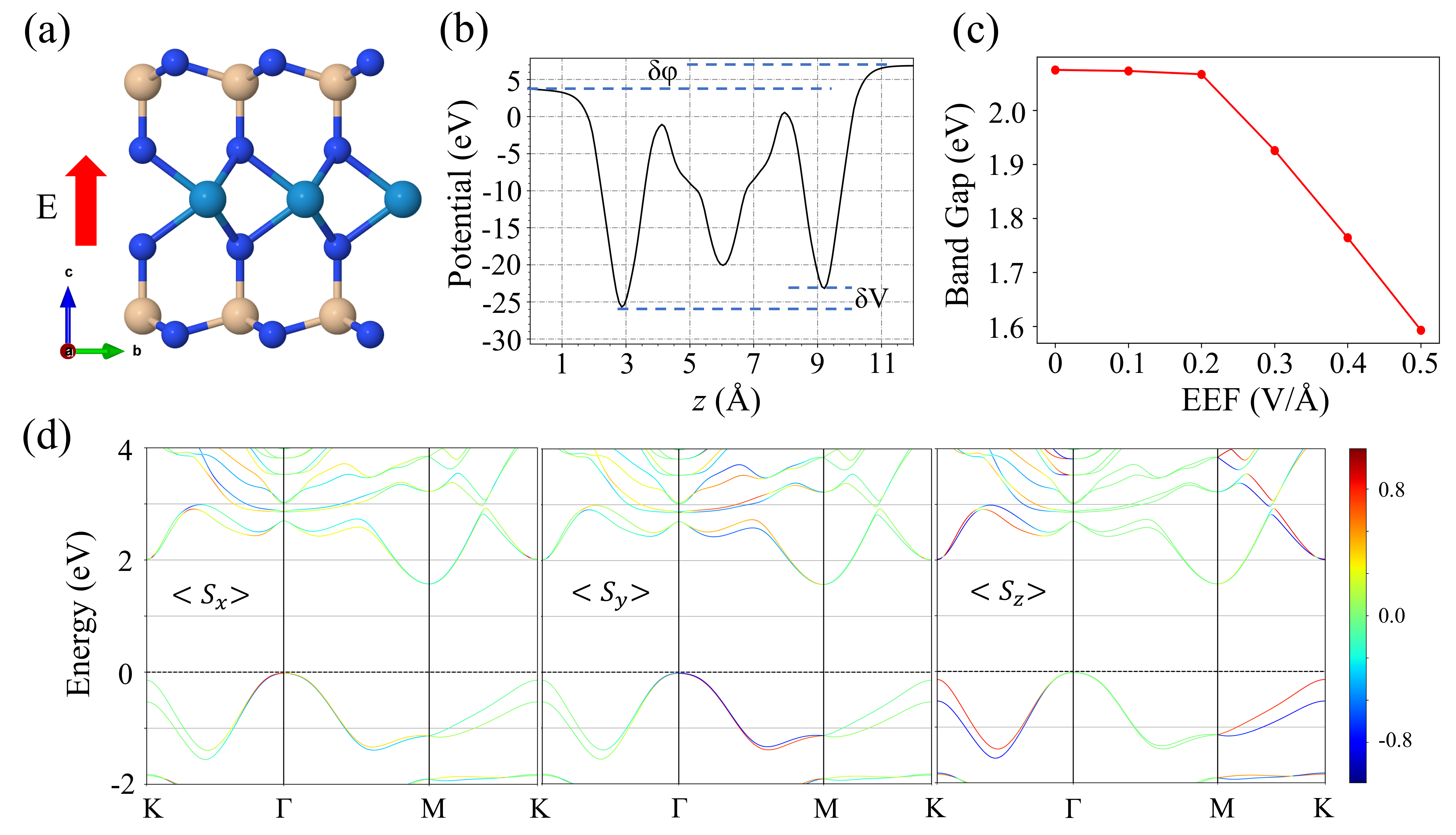
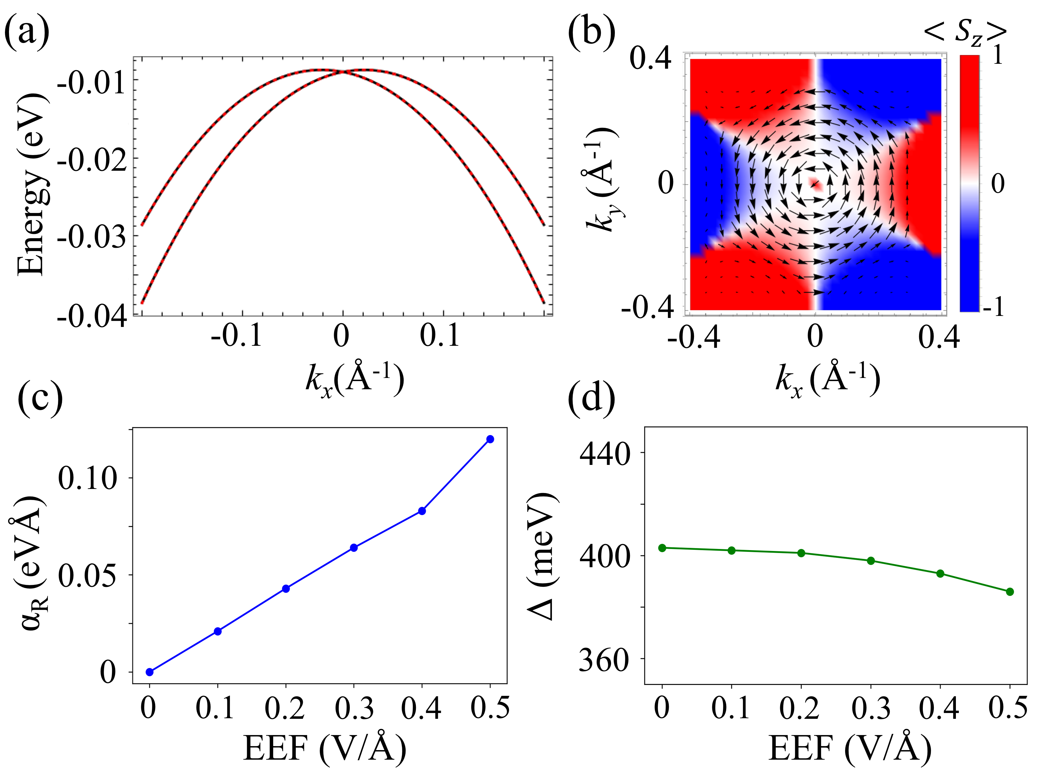
An external electric field (EEF) is always considered as an effective approach to manipulate and introduce new splittings by breaking the inversion symmetry, without changing the time-reversal invariant symmetry. Previous studies for TMDs have shown that the strength of Rashba-type splitting is tunable with the help of EEF Hu et al. (2018). To understand the effect of EEF, we theoretically apply the EEF in the range of 0 to 0.5 V/Å, in the -direction on WSi2N2, as illustrated in Fig. 5(a). Firstly, we plot the planar average of the electrostatic potential energy as a function of . In contrast to the case of without EEF, the potential energy here is asymmetric with respect to the W atom (see Fig. 5(b)). It can be easily seen that a significant potential difference ( eV) is generated between the two Si-layers. The potential energy on the upper side of Si layer is larger compared to its lower counterpart. This confirms the breaking of the surface inversion symmetry. Then, we observe the effect of EEF on band gaps, which can be explained as stark effect in condensed matter system. Our system is out-of-plane symmetric, therefore, EEF shows the same effect in both positive and negative -directions. Figure 5(c) shows the band gap variation as a function of EEF. Between 0.1 and 0.2 V/Å, the position of CBm changes from K point to the M point (see Fig. S5 in SM). The band gap is nearly constant up to 0.2 V/Å and thereafter, decreases linearly to 1.59 eV under 0.5 V/Å EEF. Figure 5(d) shows the spin projected band structure with an EEF of 0.5 V/Å. Here, we see that near VBM ( point), the out-of-plane spin component vanishes and the in-plane spin components arise. Figure 6(a) and 6(b) show the band structure around point and associated spin texture, respectively. The helical-type in-plane spin polarization confirms the existence of Rashba-type splitting.
To understand Rashba splitting, we include additional EEF dependent term in the aforementioned k.p models, which is given as
| (10) |
where is the splitting coefficient dependent on the strength of EEF. The term breaks the SIS, which reduces the point group symmetry of 2D system from to and considers the in-plane spin component. The contribution of near point is dominant as compared to cubic term, therefore, the in-plane spin component is observed near point. Furthermore, the out-of-plane component starts dominating as we move away from the point. Figure 6(c) and 6(d) show the variation of (around point) and as a function of EEF. The is linearly dependent on the EEF. Such a linear relationship helps in the precise control of spin-precession in spin field-effect transistors. When the EEF is 0.5 V/Å, the Rashba spin splitting occurs at the point with a Rashba coefficient of 0.12 eVÅ, obtained by parameterizing the Eq. 10. The observed values of are small as compared to the TMD (0.20 eVÅ) under the same EEF, since the W atom is covered by the Si-N layers. Thus, the W- orbitals contributing the VBM are less influenced by the EEF. The spin splitting and spin textures around K and M points are hardly influenced by the EEF, because the non-zero constant term around K and linear term with coefficient dominate over the . Therefore, the SOFs and are parallel to -direction and are independent of EEF. The PST preserve fully along M-K path having only the out-of-plane component of spin polarization. Therefore, PST are robust to small EEF, except around point.
III.5 Hidden spin polarization in bulk WSi2N4
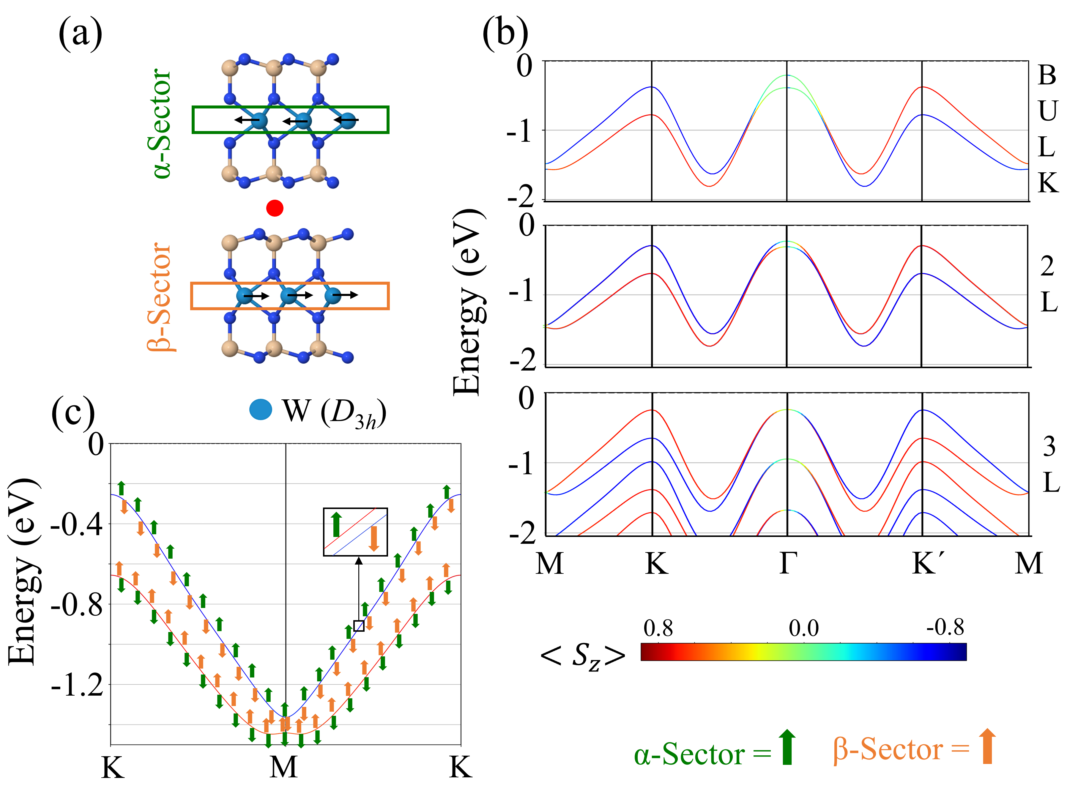
The previous theoretical study reports the possibility of experimental realization of layered bulk WSi2N4 family, using the bottom up synthesis method Islam et al. (2021). We have considered the layer dependence of the spin polarization in layered WSi2N4 family. The bulk WSi2N4 has an indirect band gap of 1.97 eV having CBm and VBM at K and , respectively Islam et al. (2021). Figure 7(a) shows the unit cell of bulk WSi2N4 having space group symmetry. The associated point group symmetry is and have a point of inversion as shown in Fig. 7(a). The presence of inversion and time reversal symmetries lead to the bands to be two-fold degenerate throughout the BZ. As expected, the top valence bands are two-fold degenerate as shown in Fig. 7(b). In current view, the Rashba and Dresselhaus effects are observed only when the inversion symmetry is absent. Thus, it is unwise to look for spin splitting and spin polarization in centrosymmetric bulk WSi2N4. Therefore, the degree of spin polarization is expected to be zero in inversion symmetric even layered and bulk WSi2N4, as reported in Ref. Islam et al. (2021). In contrast, we report the existence of hidden spin polarization for bulk WSi2N4, which can be attributed to the hidden Dresselhaus (D-2) effect Zhang et al. (2014). The key point here is that SOC is anchored on particular nuclear sites in the solid, thus it is the individual atomic site symmetry in solid that forms a good starting point to describe the SOC-induced spin-polarization. The net spin polarization of the bulk crystal is sum of the local polarization over the atomic sites. The D-2 effect arises when the site point group of an atom within a 3D crystal lacks inversion asymmetry and the crystal as a whole is centrosymmetric Zhang et al. (2014).
In present case, the inversion symmetry is present in bulk space group but not in the site point groups (see Fig. 7(a)). One such atomic site is W atom, where site point group is inversion asymmetric , contributing mainly to the low-energy spectrum. The two W layers connected by the inversion symmetry are indicated as sectors and . The two sectors are individually inversion asymmetric and produce equal dipole moment but in opposite directions (see Fig. 7(a)). Therefore, the net dipole moment of bulk WSi2N4 becomes zero, which is the central property of centrosymmetric structures. Figure 7(c) shows the band structure projected on the spin components and real space sectors and . If we consider only one sector, the large band splitting (0.4 eV) between spin-up and spin-down states is observed along K-M-K path. The interactions between the sectors form a pair of bonding and antibonding states, therefore, open a band gap at the band crossing M point Liu et al. (2015). Even though the bands are doubly degenerate as a consequence of bulk inversion asymmetry, the branches of doubly degenerate bands have opposite spin polarizations, which are separated in the real space (see Fig. 7(c)). As already discussed, is a good quantum number, therefore, the spins are fully out-of-plane and up and down spins locate at the energy bands. The weak van der Waals interaction among inversion partners causes slight spin mixture from another layer and slightly larger separation of the degenerate bands. However, most of the spin at the K valley remains on each layer. The real space segregation of spin polarized bands originates from the separate local sites Dresselhaus SOC. The bulk spin polarization in such systems can be observed by controlling the stacking directions probing beams Riley et al. (2014); Yao et al. (2017); Wu et al. (2017). The extra advantage of D-2 effect is that the spins can be controlled by manipulating the interaction between two inversion parts. One such example is that a small electric field ( mV/Å) is required to reverse the spin polarization as compared to linear Rashba effect Yuan et al. (2019).
The results similar to the bulk are expected to be observed for even number of layers of WSi2N4, having centrosymmetric space group symmetry. Therefore, we have examined the results for bilayer-WSi2N4. The real space segregated hidden spin polarization is also observed in doubly degenerate bands of topmost valence bands (see Fig.7(b)). The band splitting similar to monolayer is observed in odd number of layers of WSi2N4 having non-centrosymmetric space group symmetry (i.e. see band structure for trilyer in Fig.7(b)).
Now, let us comment on the possible applications of PST in WA2Z4 materials, which can act as channel for spin-FET. The out-of-plane spin polarization is injected through the ferromagnetic source. The SOC rotate its polarization during its path, and is either transmitted or reflected to the drain electrode depending upon the spin state, therefore, act as on or off states, respectively Schliemann (2017). The on/off functionality can be further controlled by the EEF. The observed small value of nm is promising for highly efficient devices. The coexistence of hidden spin polarization and PST is another important avenue to pursue.
IV Conclusion
We have revealed the interesting spin splitting properties of WA2Z4 family. The formation energies, phonon spectra and AIMD calculations confirm the stability of these materials. The PBE, HSE06 and the excited state methods G0W0 and BSE show that these materials are semiconducting, having a band gap in visible region. In addition to valley dependent properties at the corners of BZ, we have observed cubic and linear split bands around the time-reversal invariant and M points, respectively. The in-plane mirror symmetry () leads to out-of-plane FZPST, therefore, enabling dissipationless long range transport through spatially periodic mode PSH mechanism. The effect of EEF is duly considered on band gap and spin splitting. The EEF leads to linear Rashba-type helical spin texture around the VBM. The impact of layer thickness is studied in aforementioned effects. We have found the hidden spin polarization in the bulk and even layered WSi2N4, which can be attributed to the D-2 effect. The D-2 effect arises because the local site point of W atom lacks inversion symmetry; however, the global space group is centrosymmetric. The PST is robust to electric field and thickness along the M-K direction. We believe that this work will provide highly efficient spintronics and valleytronics devices for room temperature applications.
V Acknowledgement
S.S. acknowledges CSIR, India, for the senior research fellowship [grant no. 09/086(1432)/2019-EMR-I]. D.G. acknowledges UGC, India, for the senior research fellowship [Grant No. 1268/(CSIR-UGC NET JUNE 2018)]. A.P. acknowledges IIT Delhi for the junior research fellowship. S. B. acknowledges financial support from SERB under a core research grant (grant no. CRG/2019/000647) to set up his High Performance Computing (HPC) facility “Veena” at IIT Delhi for computational resources. We acknowledge the High Performance Computing (HPC) facility at IIT Delhi for computational resources.
References
- Geim (2009) A. K. Geim, Science 324, 1530 (2009).
- Novoselov et al. (2012) K. S. Novoselov, L. Colombo, P. Gellert, M. Schwab, and K. Kim, Nature 490, 192 (2012).
- Kane and Mele (2005) C. L. Kane and E. J. Mele, Phys. Rev. Lett. 95, 226801 (2005).
- Ni et al. (2012) Z. Ni, Q. Liu, K. Tang, J. Zheng, J. Zhou, R. Qin, Z. Gao, D. Yu, and J. Lu, Nano Lett. 12, 113 (2012).
- Molle et al. (2018) A. Molle, C. Grazianetti, L. Tao, D. Taneja, M. H. Alam, and D. Akinwande, Chem. Soc. Rev. 47, 6370 (2018).
- Chopra et al. (1995) N. G. Chopra, R. Luyken, K. Cherrey, V. H. Crespi, M. L. Cohen, S. G. Louie, and A. Zettl, Science 269, 966 (1995).
- Golberg et al. (2007) D. Golberg, Y. Bando, C. Tang, and C. Zhi, Adv. Mater. 19, 2413 (2007).
- Manzeli et al. (2017) S. Manzeli, D. Ovchinnikov, D. Pasquier, O. V. Yazyev, and A. Kis, Nat. Rev. Mater. 2, 1 (2017).
- Xu et al. (2014) X. Xu, W. Yao, D. Xiao, and T. F. Heinz, Nat. Phys. 10, 343 (2014).
- Wang et al. (2018) G. Wang, A. Chernikov, M. M. Glazov, T. F. Heinz, X. Marie, T. Amand, and B. Urbaszek, Rev. Mod. Phys. 90, 021001 (2018).
- Shuck et al. (2020) C. E. Shuck, A. Sarycheva, M. Anayee, A. Levitt, Y. Zhu, S. Uzun, V. Balitskiy, V. Zahorodna, O. Gogotsi, and Y. Gogotsi, Adv. Energy Mater. 22, 1901241 (2020).
- Zhan et al. (2020) X. Zhan, C. Si, J. Zhou, and Z. Sun, Nanoscale Horiz. 5, 235 (2020).
- Hong et al. (2020) Y.-L. Hong, Z. Liu, L. Wang, T. Zhou, W. Ma, C. Xu, S. Feng, L. Chen, M.-L. Chen, and D.-M. Sun, Science 369, 670 (2020).
- Wang et al. (2021) L. Wang, Y. Shi, M. Liu, A. Zhang, Y.-L. Hong, R. Li, Q. Gao, M. Chen, W. Ren, and H.-M. Cheng, Nat. Commun. 12, 1 (2021).
- Yang et al. (2021) C. Yang, Z. Song, X. Sun, and J. Lu, Phys. Rev. B 103, 035308 (2021).
- Huang et al. (2022) D. Huang, F. Liang, R. Guo, D. Lu, J. Wang, H. Yu, and H. Zhang, Adv. Opt. Mater. p. 2102612 (2022).
- Mortazavi et al. (2021) B. Mortazavi, B. Javvaji, F. Shojaei, T. Rabczuk, A. V. Shapeev, and X. Zhuang, Nano Energy 82, 105716 (2021).
- Pacchioni (2020) G. Pacchioni, Nat. Rev. Mater. 5, 480 (2020).
- Kang et al. (2013) J. Kang, J. Li, S.-S. Li, J.-B. Xia, and L.-W. Wang, Nano Lett. 13, 5485 (2013).
- Singh et al. (2018) S. Singh, C. Espejo, and A. H. Romero, Phys. Rev. B 98, 155309 (2018).
- He et al. (2014) J. He, K. Hummer, and C. Franchini, Phys. Rev. B 89, 075409 (2014).
- Xiao et al. (2012) D. Xiao, G.-B. Liu, W. Feng, X. Xu, and W. Yao, Phys. Rev. Lett. 108, 196802 (2012).
- Schmidt et al. (2016) H. Schmidt, I. Yudhistira, L. Chu, A. C. Neto, B. Özyilmaz, S. Adam, and G. Eda, Phys. Rev. Lett. 116, 046803 (2016).
- Ochoa et al. (2012) H. Ochoa, A. C. Neto, and F. Guinea, Phys. Rev. Lett. 108, 206808 (2012).
- Schliemann (2017) J. Schliemann, Rev. Mod. Phys. 89, 011001 (2017).
- Tao and Tsymbal (2018) L. Tao and E. Y. Tsymbal, Nat. Commun. 9, 1 (2018).
- Zhao et al. (2020) H. J. Zhao, H. Nakamura, R. Arras, C. Paillard, P. Chen, J. Gosteau, X. Li, Y. Yang, and L. Bellaiche, Phys. Rev. Lett. 125, 216405 (2020).
- Li et al. (2020) S. Li, W. Wu, X. Feng, S. Guan, W. Feng, Y. Yao, and S. A. Yang, Phys. Rev. B 102, 235435 (2020).
- Ai et al. (2021) H. Ai, D. Liu, J. Geng, S. Wang, K. H. Lo, and H. Pan, Phys. Chem. Chem. Phys. 23, 3144 (2021).
- Islam et al. (2021) R. Islam, B. Ghosh, C. Autieri, S. Chowdhury, A. Bansil, A. Agarwal, and B. Singh, Phys. Rev. B 104, L201112 (2021).
- Kresse and Furthmüller (1996) G. Kresse and J. Furthmüller, Phys. Rev. B 54, 11169 (1996).
- Blöchl (1994) P. E. Blöchl, Phys. Rev. B 50, 17953 (1994).
- Kresse and Joubert (1999) G. Kresse and D. Joubert, Phys. Rev. B 59, 1758 (1999).
- Perdew et al. (1996) J. P. Perdew, K. Burke, and M. Ernzerhof, Phys. Rev. Lett. 77, 3865 (1996).
- Perdew et al. (1998) J. Perdew, K. Burke, and M. Ernzerhof, Phys. Rev. Lett. 80, 891 (1998).
- Hedin (1965) L. Hedin, Phys. Rev. 139, A796 (1965).
- Hybertsen and Louie (1985) M. S. Hybertsen and S. G. Louie, Phys. Rev. Lett. 55, 1418 (1985).
- Monkhorst and Pack (1976) H. J. Monkhorst and J. D. Pack, Phys. Rev. B 13, 5188 (1976).
- Tkatchenko et al. (2012) A. Tkatchenko, R. A. DiStasio Jr, R. Car, and M. Scheffler, Phys. Rev. Lett. 108, 236402 (2012).
- Togo and Tanaka (2015) A. Togo and I. Tanaka, Scr. Mater. 108, 1 (2015).
- King-Smith and Vanderbilt (1993) R. D. King-Smith and D. Vanderbilt, Phys. Rev. B 47, 1651 (1993).
- Albrecht et al. (1998) S. Albrecht, L. Reining, R. Del Sole, and G. Onida, Phys. Rev. Lett. 80, 4510 (1998).
- Sheoran et al. (2022a) S. Sheoran, P. Bhumla, and S. Bhattacharya, arXiv preprint arXiv:2203.05978 (2022a).
- Jin et al. (2021) K.-H. Jin, E. Oh, R. Stania, F. Liu, and H. W. Yeom, Nano Lett. 21, 9468 (2021).
- Jia et al. (2020) F. Jia, S. Hu, S. Xu, H. Gao, G. Zhao, P. Barone, A. Stroppa, and W. Ren, J. Phys. Chem. Lett. 11, 5177 (2020).
- Bhumla et al. (2021) P. Bhumla, D. Gill, S. Sheoran, and S. Bhattacharya, J. Phys. Chem. Lett. 12, 9539 (2021).
- Sheoran et al. (2022b) S. Sheoran, M. Kumar, P. Bhumla, and S. Bhattacharya, Mater. Adv. 3, 4170 (2022b).
- Bernevig et al. (2006) B. A. Bernevig, J. Orenstein, and S.-C. Zhang, Phys. Rev. Lett. 97, 236601 (2006).
- Hu et al. (2018) T. Hu, F. Jia, G. Zhao, J. Wu, A. Stroppa, and W. Ren, Phys. Rev. B 97, 235404 (2018).
- Ai et al. (2019) H. Ai, X. Ma, X. Shao, W. Li, and M. Zhao, Phys. Rev. Mater. 3, 054407 (2019).
- Absor et al. (2017) M. A. U. Absor, I. Santoso, K. Abraha, F. Ishii, and M. Saito, Phys. Rev. B 96, 115128 (2017).
- Li et al. (2019) X. Li, S. Zhang, H. Huang, L. Hu, F. Liu, and Q. Wang, Nano Lett. 19, 6005 (2019).
- Zhang et al. (2014) X. Zhang, Q. Liu, J.-W. Luo, A. J. Freeman, and A. Zunger, Nat. Phys. 10, 387 (2014).
- Liu et al. (2015) Q. Liu, X. Zhang, H. Jin, K. Lam, J. Im, A. J. Freeman, and A. Zunger, Phys. Rev. B 91, 235204 (2015).
- Riley et al. (2014) J. M. Riley, F. Mazzola, M. Dendzik, M. Michiardi, T. Takayama, L. Bawden, C. Granerød, M. Leandersson, T. Balasubramanian, and M. Hoesch, Nat. Phys. 10, 835 (2014).
- Yao et al. (2017) W. Yao, E. Wang, H. Huang, K. Deng, M. Yan, K. Zhang, K. Miyamoto, T. Okuda, L. Li, and Y. Wang, Nat. Commun. 8, 1 (2017).
- Wu et al. (2017) S.-L. Wu, K. Sumida, K. Miyamoto, K. Taguchi, T. Yoshikawa, A. Kimura, Y. Ueda, M. Arita, M. Nagao, and S. Watauchi, Nat. Commun. 8, 1 (2017).
- Yuan et al. (2019) L. Yuan, Q. Liu, X. Zhang, J.-W. Luo, S.-S. Li, and A. Zunger, Nat. Commun. 10, 1 (2019).