Time-Reversal Even Charge Hall Effect from Twisted Interface Coupling
Abstract
Under time-reversal symmetry, a linear charge Hall response is usually deemed to be forbidden by the Onsager relation. In this work, we discover a scenario for realizing a time-reversal even linear charge Hall effect in a non-isolated two-dimensional crystal allowed by time reversal symmetry. The restriction by Onsager relation is lifted by interfacial coupling with an adjacent layer, where the overall chiral symmetry requirement is fulfilled by a twisted stacking. We reveal the underlying band geometric quantity as the momentum-space vorticity of layer current. The effect is demonstrated in twisted bilayer graphene and twisted homobilayer transition metal dichalcogenides with a wide range of twist angles, which exhibit giant Hall ratios under experimentally practical conditions, with gate voltage controlled on-off switch. This work reveals intriguing Hall physics in chiral structures, and opens up a research direction of layertronics that exploits the quantum nature of layer degree of freedom to uncover exciting effects.
Introduction
Hall effect, by its rigorous definition, refers to a transverse charge current ,
with a unidirectional or chiral nature characterized by the Hall
conductivity pseudovector Nagaosa et al. (2010). In principle, can have two parts that are odd and even respectively under time
reversal (TR). The TR-odd part, such as the ordinary Hall effect induced by
Lorentz force and the anomalous Hall effect induced by the momentum space
Berry curvature (Fig. 1a), is obviously forbidden in TR
symmetric systems. The TR-even part is also forbidden under TR symmetry, with a more delicate origin in the Onsager relation of electrical conductivity Nagaosa et al. (2010); Onsager (1931). Therefore, the linear-response charge Hall transport has been observed only in
materials with TR breaking by magnetic field or magnetic order Nagaosa et al. (2010); Weng et al. (2015); Liu et al. (2016).
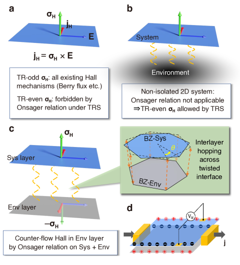
For a non-isolated system, however, the Onsager relation on electrical conductivity is not necessarily applicable Onsager (1931), depending on the form of its interplay with the environment. This in fact leaves room for the TR-even contribution to in the system, and hence the possibility of having charge Hall effect under TR symmetry (Fig. 1b). If the system is geometrically separated from the environment for the Hall voltage to be measurable, the TR-even Hall effect can have real impact, besides being fundamentally intriguing.
A platform to explore the above scenario is naturally provided in twisted van der Waals (vdW) layered structures Andrei and MacDonald (2020); Balents et al. (2020); Kennes et al. (2021); Andrei et al. (2021); Lau et al. (2022); Wilson et al. (2021); Regan et al. (2022), where a two-dimensional (2D) crystal is separated by the vdW gap from adjacent layers constituting its environment (Fig. 1c). With the demonstrated capability to access electrical conduction in individual layers of the vdW structures Gorbachev et al. (2012); Liu et al. (2017a); Sanchez-Yamagishi et al. (2017); Liu et al. (2019, 2022, 2017b), this definition of system and environment becomes physical. The restriction by Onsager relation on the system layer’s conduction is lifted by quantum tunneling of electrons across the vdW gap. Without magnetic field or magnetic order, nevertheless, chiral structural symmetry is required instead to comply with the chiral nature of Hall current. This is fulfilled in a twisted stacking that breaks inversion and all mirror symmetries Stauber et al. (2020). The intriguing TR-even Hall effect, nonetheless, remains unexplored.
In this work, we demonstrate the TR-even charge Hall effect in a twisted double layer with TR symmetry. Hall transport and
charge accumulations at edges are made possible in an individual layer.
Meanwhile, the Onsager relation for the whole double-layer geometry demands an opposite Hall
flow in the environment layer (Fig. 1c).
We find that the TR-even Hall response here is rooted in a band geometric quantity – the momentum space
vorticity of layer current – that emerges from the interlayer hybridization of
electronic states under TR and chiral symmetry.
Our symmetry analyses show that the effect is
characteristic of general chiral bilayers with Fermi surface,
which we quantitatively demonstrate for the exemplary systems of twisted bilayer graphene (tBG) and twisted homobilayer transition metal dichalcogenides (tTMDs) with a wide range of twist angles. Within experimentally feasible range of carrier doping Sui et al. (2015); Nam et al. (2017), we find pronounced Hall responses accompanied by giant Hall ratios (e.g., in tBG), with sign and magnitude controlled by the twist
angle. The effects in tTMDs also feature good on-off switchability by
gate voltage that promises device applications.
Results
Symmetry characters.
The charge Hall counterflow in system and environment layers leads to accumulation of interlayer charge dipoles (i.e., opposite charges in the two layers) near the transverse edges (Fig. 1d). Accordingly, it can be holistically viewed as the Hall transport of the charge dipole moment. The dipole Hall current measures the difference of the Hall flows in the two layers, i.e., . Onsager relation forbids a net charge Hall current counting both layers, , therefore,
| (1) |
where quantifies the charge Hall effect in the system/environment layer (Fig. 1c). Such a perspective is particularly useful for identifying the symmetry requirements for the appearance of the TR-even Hall effect as elaborated in the following.
The dipole current generated at the linear order of a driving electric field E is given by , where the Einstein summation convention is adopted for in-plane Cartesian Coordinates and , and is the current along the direction of the out-of-plane interlayer dipole moment. Since the dipole current is odd under TR while the electric field is even, in nonmagnetic metallic states, the effect can only stem from nonequilibrium kinetics of electrons around the Fermi surface, and the resulting is a TR-even tensor. The dipole Hall conductivity, which is antisymmetric with respect to the directions of the in-plane driving field and response current, is dual to that transforms as a pseudoscalar (the component of a TR-even pseudotensor). Namely, it remains unchanged under rotation, but changes sign under space inversion, mirror reflection, and roto-reflection. Such a dipole Hall effect under TR symmetry is therefore allowed provided that the bilayer crystal structure is chiral.
This chiral symmetry requirement is fulfilled in the twisted bilayer vdW structures, such as tBG and tTMDs. These most studied structures, which are also our foci, are based on honeycomb lattices and preserve the threefold rotation symmetry in the direction. This symmetry forbids the off-diagonal components of the symmetric part of with respect to and , i.e., . Therefore, according to Eq. (1), the TR-even charge Hall current in the system layer is quantified by
| (2) |
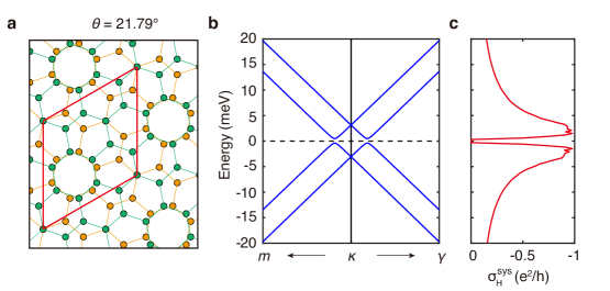
We point out that the direction of Hall current can be reversed with an opposite twist direction (Fig. 2d). This can be easily understood by noticing that structures obtained with twist angle and are mirror images of each other, whereas the mirror operation flips the sign of the Hall current in each layer.
General theory: k-space vorticity of layer current. The current density in the system and environment layer is given by the integral of the layer resolved current carried by each electron weighted by the distribution function :
| (3) |
where and are the band index and crystal momentum. , with and being respectively the projection operator onto the system and environment layer, and operating in the layer index subspace Xu et al. (2014). Because of the TR symmetry, , hence a nonzero layer current requires a distribution function in -space that breaks the occupation symmetry at and . Such an off-equilibrium distribution can be driven by an electric field and described by the Boltzmann transport equation. Within the simplest constant relaxation time approximation, the deviation from the equilibrium Fermi distribution is of a dipole structure in -space: , with being the band energy and the transport relaxation time. This approximation is usually taken so that the specific content of disorder often unknown does not pose a difficulty and that the band origin of the effect can be manifested Xie and MacDonald (2021); Sodemann and Fu (2015); Lai et al. (2021).
We focus on the TR-even charge Hall response in the system layer in the following. The Hall conductivity reads
| (4) |
where
| (5) |
is intrinsic to the band structure, has the dimension of frequency, and is indeed a TR-even pseudoscalar conforming to the symmetry analysis. Here , and implies that the TR-even Hall effect is a Fermi surface property. If interlayer coupling is absent, one has , hence no TR-even Hall effect. Similarly, the Hall conductivity of the environment layer can be obtained by replacing in with . It is clear that and the total charge Hall current of a bilayer geometry is indeed vanishing. The formal theory thus confirms the conclusions of the foregoing symmetry arguments.
Now we show that the TR-even Hall effect has a band origin in the k-space vorticity of the layer current. Via integration by parts, Eq. (5) is recast into
| (6) |
which measures the k-space vorticity of the layer current integrated over the occupied states. As the integral of this vorticity over any full band vanishes, only of partially occupied bands contribute to a net TR-even Hall effect. The layer current vorticity can be expressed in an enlightening form
| (7) |
where the numerator involves interband matrix elements of total velocity and layer velocity operators. Under the TR operation, interband quantities are transformed into their complex conjugates and is even, with which one finds that is also TR-even after taking the real part. This expression of shares a striking similarity with the well-known band geometric quantity k-space Berry curvature Xiao et al. (2010): The former becomes the latter if is replaced by the -space interband Berry connection . As such, the TR-even Hall effect, despite being described by the Boltzman transport theory, encodes the information of interband coherence, which has up to now mostly connected to intrinsic transport effects induced by various Berry-phase effects Nagaosa et al. (2010); Sinova et al. (2015); Schaibley et al. (2016); Xiao et al. (2010), and hence should be enhanced when the Fermi level is located around band near-degeneracy regions. Despite the similarity, we stress that the layer current vorticity is fundamentally different from the k-space Berry curvature – The latter is TR-odd and is directly involved in the noncanonical dynamical structure of semiclassical Bloch electrons Xiao et al. (2010), while results from electric field-induced Fermi surface shift.
It is also interesting to note that , where . Being the imaginary part of , the -space vorticity of the layer current is connected to the real-space circulation of this current around the electron wave-packet center Xiao et al. (2010): . While stems from the self-rotational motion of the electron wave packet, results from the center-of-mass motion. Their relation is analogous to the -space Berry curvature and quantum metric, which are the imaginary and real parts of the quantum geometric tensor Ma et al. (2010).
Nonzero layer current vorticity and a net flux require the quantum interlayer hybridization of electronic states, which is a characteristic property not shared by Berry curvature. First, in the absence of layer-hybridized states, would vanish. Two scenarios of full layer polarization leading to vanishing can be immediately identified: (i) If the states and involved in Eq. (7) are fully polarized in the same layer around some , one gets and thus . (ii) If the two states are fully polarized in different layers, then , and hence also . Moreover, by comparing the two forms of in Eqs. (5) and (6), one directly sees that a finite flux of vorticity also requires interlayer hybridization – If is fully layer-polarized, one has , so and in Eq. (5).
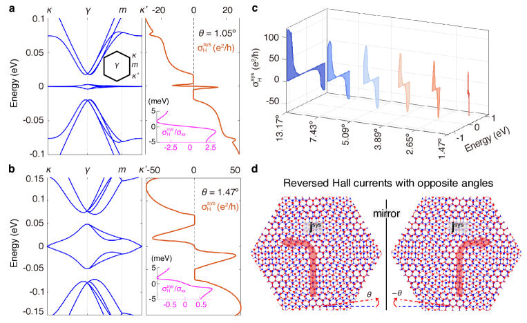
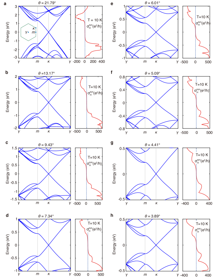
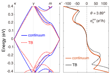
Application to tBG. We now apply our theory to tBG. For small twist angles , we employ the continuum model with parameters taken from Ref. Koshino et al. (2018). The results are corroborated by tight-binding calculations, which are also applicable at large . All model details are presented in the Methods section and Supplementary Note 2 and 3.
The calculation results for and are shown in Figs. 2a and b. The central bands around zero energy are separated from their neighbors with a global gap at such small angles. When the Fermi level intersects the central bands, shows two narrow peaks with opposite signs for electron and hole doping. When the Fermi level is located in the global gap, vanishes as a Fermi surface property. Its magnitude starts to increase again when the Fermi level is shifted outside the gap. Assuming a relaxation time of 1 ps Wang et al. (2013); Schmitz et al. (2017); Sun et al. (2021), the TR-even Hall conductivity can reach dozens of upon Fermi level shifts within 20 meV. Such slight shifts can be readily achieved by dual gates. The experimental measurement shall also be facilitated by a large Hall ratio , which is independent of the relaxation time if the longitudinal charge conductivity is also evaluated using the constant approximation. In the current case, is strongly suppressed by the quite flat dispersion, thus the Hall ratio can be , as shown in the inset of Figs. 2a and b.
The TR-even Hall effect is not restricted to long-wavelength moiré lattices. When gets large, the profiles of remain similar, but the width and magnitude of its peaks increase. This is illustrated in Fig. 2c, where the central peaks of are presented for a series of . While the two peaks become more separated as increases, sizable within dozens of meV around zero-energy is still achievable for a wide range of .
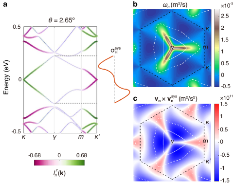
Next we look at the k-space distributions of layer composition and layer current vorticity to have a better understanding of the features of the TR-even Hall effect. We illustrate these in Fig. 3 using a tBG and focus on the first conduction band. The band projection of the layer composition is denoted by color in Fig. 3a. At low energies, the layer hybridization is weak, thus the states are dominantly system/environment (or top/bottom) layer polarized around /. At higher energies, Dirac cones from the two layers intersect and hybridize strongly around the point, rendering . Such layer polarizations or hybridizations in different band regions are also manifested in Fig. 3b for the distribution of the layer current vorticity. It is concentrated along the path from to , which is characterized by regions with strongly layer-hybridized and nearly-degenerate bands, and is suppressed in the layer polarized regions around and . White curves in Fig. 3b show two different Fermi surfaces. At low electron doping, is contributed by the dark blue area in Fig. 3b with , thus it is negative and increases in magnitude as the Fermi level is lifted towards the middle of the band [see Eq. (6) and brown curve in Fig. 3a]. As the Fermi level is further increased, regions with highly concentrated start to contribute, hence the magnitude of drops. Evolution of with the Fermi level can also be understood from the distribution of shown in Fig. 3c. Since it is dominantly negative in the blue regions, according to Eq. (5), shall be negative and maximal when the Fermi level locates around the middle of the band.
In a long-wavelength moiré, the two valleys contribute to the layer Hall conductivity with identical sign and magnitude [see Eq. (7)], therefore intervalley scattering in tBG Phinney et al. (2021) is not expected to diminish the effect. When the twist angle gets large enough, Umklapp process becomes important Mele (2010); Park et al. (2019), and can hybridize the two valleys and lead to new features in the layer Hall conductivity that are not expected from the continuum model. Our tight-binding calculations for shows that Umklapp process leads to emergence of new conductivity peaks at low energies (see Supplementary Fig. 3).
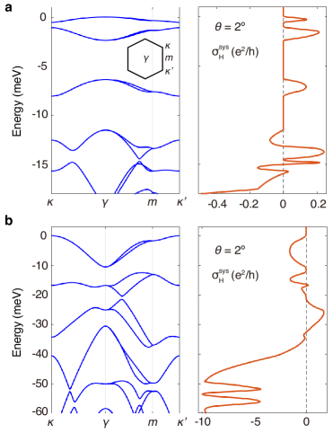
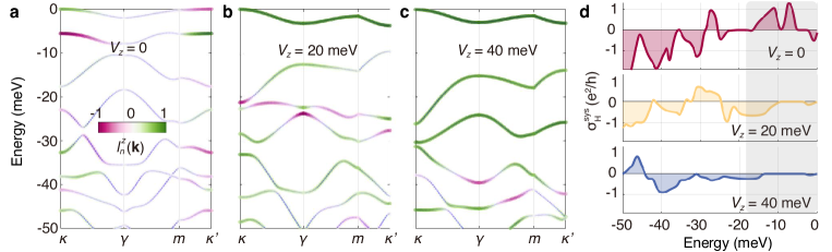
Application to tTMDs. Now we briefly address the TR-even Hall effect in tTMDs and focus on its tuning. We consider the continuum model of tMoTe2 Wu et al. (2019); Yu et al. (2020) as an example (see Supplementary Note 1). The calculation results for and are shown in Fig. 4. The obtained TR-even Hall conductivity can reach and the Hall ratio . It exhibits rich profiles, which can be attributed to the complexity of tTMDs band structures that feature multiple isolated narrow bands, and the efficient layer hybridization in this material. As is shown in Fig. 5a for the case of , most band regions are strongly layer hybridized.
Properties of tTMDs can be sensitively tuned via the interlayer bias . The band structures of tMoTe2 with different are shown in Figs. 5a–c, and the corresponding TR-even Hall conductivities are presented in Fig. 5d. The profiles of vary dramatically for different , including the magnitude and sign. A prominent impact of interlayer bias is the suppression of at low energies (grey area in Fig. 5d), which indicates that the TR-even Hall effect can be turned on/off with gate control. This is because the interlayer bias polarizes low-energy electrons into one of the layers (see the dominance of green color in Figs. 5b and c), thus reduces interlayer coupling.
This gate suppressed TR-even Hall effect totally differs from the gate induced
layer-polarized Hall effect appearing in the even-layer antiferromagnet
MnBi2Te4 Gao et al. (2021); Chen et al. . This distinction arises from the
fact that the former and latter effects favor strong layer hybridization and
layer polarization, respectively. It is also noted that the linear Hall effect
in a nonmagnetic bilayer can only appear in the layer-counterflow manner in
line with the Onsager relation (Fig. 1c), irrespective of the gate voltage;
while the layer-resolved Hall effects in top and bottom ferromagnetic layers of
antiferromagnetic bilayer MnBi2Te4 can be quite different when the
combined symmetry of TR and space inversion is broken by the gate.
Discussion
In summary, we have discovered the TR-even linear charge Hall effect in a non-isolated 2D crystal endowed by the twisted interfacial coupling to an environmental layer, and elucidated the band origin of this effect. Measurable effects with great tunability are predicted in paradigmatic twisted bilayer materials in the presence of TR symmetry.
The layer Hall counterflow here contrasts with spin/valley Hall effect Sinova et al. (2015); Schaibley et al. (2016); Xiao et al. (2010), in the latter counterflowing Hall currents for opposite spin/valley are spatially not separated so that it is impossible to access a charge Hall current. Here, the charge Hall current in each layer is experimentally accessible with the layer-contrasted geometry in vdW devices (see Supplementary Note 5).
It is also noted that the physics revealed is fundamentally distinct from the layer-polarized Hall effect in
layered antiferromagnetic insulators Gao et al. (2021); Chen et al. ; Peng et al. ; Dai et al. and
the layer-dependent quantum Hall effect Gorbachev et al. (2012); Liu et al. (2017a); Sanchez-Yamagishi et al. (2017); Liu et al. (2019, 2022, 2017b), both of which rely on the TR symmetry breaking, and from the nonlinear Hall effects Sodemann and Fu (2015); Lai et al. (2021); Du et al. (2021) where the Onsager relation is obviously
irrelevant.
We note that in second-order nonlinear Hall effect, there also exists a TR-even band quantity – Berry curvature dipole Du et al. (2021). It, however, has different symmetry constraints from the -space vorticity of layer current. In particular, it is forbidden by the threefold rotational symmetry in 2D systems, and thus is absent in tBG and tTMDs studied here.
In the absence of magnetization and magnetic field, the sign of the linear Hall voltage now can be determined by the chirality of the interface, represented by the sign of the twisting angle. The effect therefore also serves as an efficient electrical probe on the structural chirality.
Methods
Continuum model of tBG and tTMDs.
The top and bottom layers are rotated counterclockwise by , respectively, with the corresponding rotation matrix . In tBG, the Hamiltonian for +K valley around reads Koshino et al. (2018)
| (8) |
where Å, m/s, and with and the Pauli matrices in sublattice space. and are Dirac points after rotation in the top and bottom layer, respectively. The moiré modulated interlayer tunneling is modeled by , where
| (9) |
and are the moiré reciprocal lattice vectors, with the moiré period. The interlayer tunneling constants are meV and meV Koshino et al. (2018). The Hamiltonian from the -K valley can be obtained from TR operation.
The continuum model of tTMDs is very similar to that of tBG, with additional electrostatic modulations in each layer Wu et al. (2019); Yu et al. (2020). We leave its details to the Supplementary Note 1.
Tight-binding model of tBG. To characterize the electronic structures and TR-even Hall effect of tBG, we also use a tight-binding model following Ref. Moon and Koshino (2013). The Hamiltonian is given by
| (10) |
where and are the creation and annihilation operators for the orbital on site and , represents the position vector from site to , and is the hopping amplitude between sites and . We adopt the following approximations
| (11) |
In the above, Å is the nearest-neighbor distance on monolayer graphene, Å is the interlayer spacing, is the intralayer hopping energy between nearest-neighbor sites, and is that between vertically stacked atoms on the two layers. Here we take eV, eV, is the decay length of the hopping amplitude and is set to 0.45255 Å. The hopping for Å is exponentially small thus is neglected in our study.
Acknowledgements
We thank Xu-Tao Zeng for helpful discussions and Chengxin Xiao for the assistance of preparing figure 1.
This work is supported by the Research Grant Council of Hong Kong (AoE/P-701/20, W.Y.; HKU SRFS2122-7S05, W.Y.),
and the Croucher Foundation (Croucher Senior Research Fellowship, W.Y.). W.Y. also acknowledges support by Tencent Foundation.
References
- Nagaosa et al. (2010) N. Nagaosa, J. Sinova, S. Onoda, A. H. MacDonald, and N. P. Ong, Rev. Mod. Phys. 82, 1539 (2010).
- Onsager (1931) L. Onsager, Phys. Rev. 37, 405 (1931).
- Weng et al. (2015) H. Weng, R. Yu, X. Hu, X. Dai, and Z. Fang, Advances in Physics 64, 227 (2015).
- Liu et al. (2016) C.-X. Liu, S.-C. Zhang, and X.-L. Qi, Annual Review of Condensed Matter Physics 7, 301 (2016).
- Andrei and MacDonald (2020) E. Y. Andrei and A. H. MacDonald, Nat. Mater. 19, 1265 (2020).
- Balents et al. (2020) L. Balents, C. R. Dean, D. K. Efetov, and A. F. Young, Nat. Phys. 16, 725 (2020).
- Kennes et al. (2021) D. M. Kennes, M. Claassen, L. Xian, A. Georges, A. J. Millis, J. Hone, C. R. Dean, D. N. Basov, A. N. Pasupathy, and A. Rubio, Nat. Phys. 17, 155 (2021).
- Andrei et al. (2021) E. Y. Andrei, D. K. Efetov, P. Jarillo-Herrero, A. H. MacDonald, K. F. Mak, T. Senthil, E. Tutuc, A. Yazdani, and A. F. Young, Nat. Rev. Mater. 6, 201 (2021).
- Lau et al. (2022) C. N. Lau, M. W. Bockrath, K. F. Mak, and F. Zhang, Nature 602, 41 (2022).
- Wilson et al. (2021) N. P. Wilson, W. Yao, J. Shan, and X. Xu, Nature 599, 383 (2021).
- Regan et al. (2022) E. C. Regan, D. Wang, E. Y. Paik, Y. Zeng, L. Zhang, J. Zhu, A. H. MacDonald, H. Deng, and F. Wang, Nat. Rev. Mater. (2022), 10.1038/s41578-022-00440-1.
- Gorbachev et al. (2012) R. V. Gorbachev, A. K. Geim, M. I. Katsnelson, K. S. Novoselov, T. Tudorovskiy, I. V. Grigorieva, A. H. MacDonald, S. V. Morozov, K. Watanabe, T. Taniguchi, and L. A. Ponomarenko, Nat. Phys. 8, 896 (2012).
- Liu et al. (2017a) X. Liu, K. Watanabe, T. Taniguchi, B. I. Halperin, and P. Kim, Nat. Phys. 13, 746 (2017a).
- Sanchez-Yamagishi et al. (2017) J. D. Sanchez-Yamagishi, J. Y. Luo, A. F. Young, B. M. Hunt, K. Watanabe, T. Taniguchi, R. C. Ashoori, and P. Jarillo-Herrero, Nat. Nanotechnol. 12, 118 (2017).
- Liu et al. (2019) X. Liu, Z. Hao, K. Watanabe, T. Taniguchi, B. I. Halperin, and P. Kim, Nat. Phys. 15, 893 (2019).
- Liu et al. (2022) X. Liu, J. I. A. Li, K. Watanabe, T. Taniguchi, J. Hone, B. I. Halperin, P. Kim, and C. R. Dean, Science 375, 205 (2022).
- Liu et al. (2017b) X. Liu, L. Wang, K. C. Fong, Y. Gao, P. Maher, K. Watanabe, T. Taniguchi, J. Hone, C. Dean, and P. Kim, Phys. Rev. Lett. 119, 056802 (2017b).
- Stauber et al. (2020) T. Stauber, J. González, and G. Gómez-Santos, Phys. Rev. B 102, 081404 (2020).
- Sui et al. (2015) M. Sui, G. Chen, L. Ma, W.-Y. Shan, D. Tian, K. Watanabe, T. Taniguchi, X. Jin, W. Yao, D. Xiao, and Y. Zhang, Nature Physics 11, 1027 (2015).
- Nam et al. (2017) Y. Nam, D.-K. Ki, D. Soler-Delgado, and A. F. Morpurgo, Nature Physics 13, 1207 (2017).
- Xu et al. (2014) X. Xu, W. Yao, D. Xiao, and T. F. Heinz, Nature Physics 10, 343 (2014).
- Xie and MacDonald (2021) M. Xie and A. H. MacDonald, Phys. Rev. Lett. 127, 196401 (2021).
- Sodemann and Fu (2015) I. Sodemann and L. Fu, Phys. Rev. Lett. 115, 216806 (2015).
- Lai et al. (2021) S. Lai, H. Liu, Z. Zhang, J. Zhao, X. Feng, N. Wang, C. Tang, Y. Liu, K. S. Novoselov, S. A. Yang, and W.-b. Gao, Nature Nanotechnology 16, 869 (2021).
- Xiao et al. (2010) D. Xiao, M.-C. Chang, and Q. Niu, Rev. Mod. Phys. 82, 1959 (2010).
- Sinova et al. (2015) J. Sinova, S. O. Valenzuela, J. Wunderlich, C. H. Back, and T. Jungwirth, Rev. Mod. Phys. 87, 1213 (2015).
- Schaibley et al. (2016) J. R. Schaibley, H. Yu, G. Clark, P. Rivera, J. S. Ross, K. L. Seyler, W. Yao, and X. Xu, Nature Reviews Materials 1, 1 (2016).
- Ma et al. (2010) Y.-Q. Ma, S. Chen, H. Fan, and W.-M. Liu, Phys. Rev. B 81, 245129 (2010).
- Koshino et al. (2018) M. Koshino, N. F. Q. Yuan, T. Koretsune, M. Ochi, K. Kuroki, and L. Fu, Phys. Rev. X 8, 031087 (2018).
- Wang et al. (2013) L. Wang, I. Meric, P. Y. Huang, Q. Gao, Y. Gao, H. Tran, T. Taniguchi, K. Watanabe, L. M. Campos, D. Muller, J. Guo, P. Kim, J. Hone, K. L. Shepard, and C. R. Dean, Science 342, 614 (2013).
- Schmitz et al. (2017) M. Schmitz, S. Engels, L. Banszerus, K. Watanabe, T. Taniguchi, C. Stampfer, and B. Beschoten, Applied Physics Letters 110, 263110 (2017).
- Sun et al. (2021) L. Sun, Z. Wang, Y. Wang, L. Zhao, Y. Li, B. Chen, S. Huang, S. Zhang, W. Wang, D. Pei, H. Fang, S. Zhong, H. Liu, J. Zhang, L. Tong, Y. Chen, Z. Li, M. H. Rümmeli, K. S. Novoselov, H. Peng, L. Lin, and Z. Liu, Nature Communications 12, 2391 (2021).
- Phinney et al. (2021) I. Y. Phinney, D. A. Bandurin, C. Collignon, I. A. Dmitriev, T. Taniguchi, K. Watanabe, and P. Jarillo-Herrero, Phys. Rev. Lett. 127, 056802 (2021).
- Mele (2010) E. J. Mele, Phys. Rev. B 81, 161405 (2010).
- Park et al. (2019) M. J. Park, Y. Kim, G. Y. Cho, and S. Lee, Phys. Rev. Lett. 123, 216803 (2019).
- Wu et al. (2019) F. Wu, T. Lovorn, E. Tutuc, I. Martin, and A. H. MacDonald, Phys. Rev. Lett. 122, 086402 (2019).
- Yu et al. (2020) H. Yu, M. Chen, and W. Yao, Natl. Sci. Rev. 7, 12 (2020).
- Gao et al. (2021) A. Gao, Y.-F. Liu, C. Hu, J.-X. Qiu, C. Tzschaschel, B. Ghosh, S.-C. Ho, D. Bérubé, R. Chen, H. Sun, et al., Nature 595, 521 (2021).
- (39) R. Chen, H.-P. Sun, M. Gu, C.-B. Hua, Q. Liu, H.-Z. Lu, and X. C. Xie, arXiv:2206.10905 .
- (40) R. Peng, T. Zhang, Z. He, Q. Wu, Y. Dai, B. Huang, and Y. Ma, arXiv:2206.14440 .
- (41) W.-B. Dai, H. Li, D.-H. Xu, C.-Z. Chen, and X. C. Xie, arXiv:2206.09635 .
- Du et al. (2021) Z. Z. Du, H.-Z. Lu, and X. C. Xie, Nat. Rev. Phys. 3, 744 (2021).
- Moon and Koshino (2013) P. Moon and M. Koshino, Phys. Rev. B 87, 205404 (2013).
Supplementary Information
Supplementary Note 1 Continuum model of near twisted homobilayer TMDs
We assume that the top and bottom layers are rotated counterclockwise by respectively with the corresponding rotation matrix . The Hamiltonian reads
| (1) |
around for spin up carriers. Note that here zero energy is set at valence band edge. In the following, we consider MoTe2, and use the parameters Å, m/s, monolayer band gap eV Wu et al. (2019). The rest of the notations are consistent with those in tBG in the Methods. To incorporate effects of interlayer bias, one adds and to the two diagonal blocks, respectively.
The electrostatic modulation in the diagonal terms of are given by with
| (2) |
where meV, meV, , and in the case of MoTe2 Wu et al. (2019). Same as the case of tBG in the Methods section, , , and .
The interlayer tunneling terms in the off-diagonal terms of are given by
| (3) |
where meV, meV, and meV in the case of MoTe2 Wu et al. (2019).
We assign the Hamiltonian in the above as the +K valley in the main text. The Hamiltonian from the -K valley can be obtained from TR operation.
Supplementary Note 2 Tight-binding model results for tBG
Supplementary Figure 1 shows the band structures and corresponding TR-even Hall conductivity in tBG from tight-binding calculations.
Supplementary Note 3 Comparison of results from continuum and tight-binding models in tBG
Supplementary Figure 2 shows the comparison of energy bands and TR-even Hall conductivity of tBG obtained from continuum model and tight-binding calculations. It is clear that the two methods yield consistent results. It should be noted that we have taken into account the effect of lattice relaxation in the continuum model by setting different values for interlayer tunneling between same-atom sites and different-atom sites Koshino et al. (2018). While such effect is not included in tight-binding calculations. Better agreement could be achieved if such effect is considered or neglected Moon and Koshino (2013) in both methods.
Supplementary Note 4 Effects of Umklapp intervalley process in tBG
Umklapp process becomes prominent near the Dirac points at large commensurate twist angles (e.g., ) Mele (2010); Park et al. (2019). To examine the effect of Umklapp process, we have performed the tight-binding calculation for tBG at (Supplementary Figure 3). The obtained energy spectrum shows gap opening at the Dirac points (Supplementary Figure 3b), which is consistent with previous results Moon and Koshino (2013); Park et al. (2019). Remarkably, the Hall conductivity shows new features (Supplementary Figure 3c) that are not expected from the continuum model. Note that the trend found in the small regime is that the conductivity peaks move to higher energy with the increase of and have opposite signs in the conduction and valence bands (Figure 2c of main text). At , however, new conductivity peaks emerge at low energies with the same sign in the conduction and valence bands (Supplementary Figure 3c). This can be attributed to the Umklapp process.
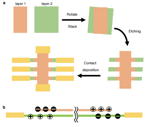
Supplementary Note 5 Proposal of experimental setup
Fabrication of electrical contacts to one individual layer for layer-resolved measurement is experimentally feasible in coupled bilayer systems. Supplementary Figure 4a shows the schematics of the experimental setup. When two monolayer flakes with different sizes/shapes are stacked, and etched into a Hall bar geometry, the overlapped part (twisted bilayer region) serves as the main channel connected to the source-drain contacts. Meanwhile, individual contacts can be deposited onto the monolayer parts of the Hall bar, which can be used as layer-resolved Hall voltage probes.
We notice that certain quantitative experimental uncertainties may exist, but they are not expected to qualitatively affect the observation. As a result of the predicted layer contrasted Hall effect, charges accumulate on the edges with layer and edge dependent signs (Supplementary Figure 4b). The interface between the bilayer and monolayer regions on the Hall bar arms can have quantitative effect on the charge distribution in the measured layer (green layer in Supplementary Figure 4), hence the transverse voltage drop measured by the electrical probes may deviate from the value predicted by our bulk theory without considering these details. However, order-of-magnitude reduction of the predicted effect is not expected when the contacts are close to the bilayer area.