Current Paths in an Atomic Precision Advanced Manufactured Device Imaged by Nitrogen-Vacancy Diamond Magnetic Microscopy
Abstract
The recently-developed ability to control phosphorous-doping of silicon at an atomic level using scanning tunneling microscopy (STM), a technique known as atomic-precision-advanced-manufacturing (APAM), has allowed us to tailor electronic devices with atomic precision, and thus has emerged as a way to explore new possibilities in Si electronics. In these applications, critical questions include where current flow is actually occurring in or near APAM structures as well as whether leakage currents are present. In general, detection and mapping of current flow in APAM structures are valuable diagnostic tools to obtain reliable devices in digital-enhanced applications. In this paper, we performed nitrogen-vacancy (NV) wide-field magnetic imaging of stray magnetic fields from surface current densities flowing in an APAM test device over a mm-field of view with m-resolution. To do this, we integrated a diamond having a surface NV ensemble with the device (patterned in two parallel mm-sized ribbons), then mapped the magnetic field from the DC current injected in the APAM device in a home-built NV wide-field microscope. The 2D magnetic field maps were used to reconstruct the surface current density, allowing us to obtain information on current paths, device failures such as choke points where current flow is impeded, and current leakages outside the APAM-defined P-doped regions. Analysis on the current density reconstructed map showed a projected sensitivity of 0.03 A/m, corresponding to a smallest detectable current in the 200 m-wide APAM ribbon of 6 A. These results demonstrate the failure analysis capability of NV wide-field magnetometry for APAM materials, opening the possibility to investigate other cutting-edge microelectronic devices.
I Introduction
Atomic-precision control over crystalline Si synthesis and processing are putting pure quantum mechanics phenomena (e.g. spin and tunnel effects) on the Si device engineer’s palette of reliable options for creating new microelectronics. One recent addition [1, 2] to the palette is a technique known as atomic-precision advanced manufacturing (APAM). A typical APAM process first creates a lithographic pattern of Si dangling bonds on a hydrogen-passivated crystalline Si surface, using scanning tunneling microscopy (STM). Next, the Si surface is exposed to phosphine gas that selectively adsorbs on sites where Si dangling bonds have been exposed, leading to atomically-precise planar structures made of P-donors [3, 4]. APAM allows us to dope Si in full 2D atomic-precision [5, 6, 7, 8, 9], to form structures such as wires [10, 5], quantum dots [11], and few- and single-dopant features [12, 13] with lattice-site (3.8 Å) control [9]. Doped features can be positioned, arrayed, coupled, and gated with atomic precision to form tunnel junctions [14], single-atom transistors [12], and a host of other possibilities, all compatible with near-standard CMOS manufacturing [6, 7, 15]. This gives us an exciting tool to explore far-reaching ideas, such as quantum computing [8], quantum simulation [16], and digital electronics that incorporate controlled quantum effects into Si foundry-compatible platforms [6, 8, 7, 17, 18].
Currently, APAM devices work only in cryogenic conditions, hence their use is limited to applications where low temperatures are required (e.g. in quantum computing) to achieve long coherence times. Realizing broader possible applications for APAM techniques in room-temperature conventional electronics is a big challenge, as it requires understanding of carrier transport in ultrathin high-density P-doped Si structures. Electronic transport in APAM-doped materials and structures has been investigated and understood at cryogenic conditions ( 4.2 K) [19]. APAM-doped regions would dominate carrier transport just by virtue of the high APAM doping levels ( cm-3), while doping in surrounding Si was kept sufficiently low ( cm-3, i.e. the metal-insulator transition) that leakage paths through the substrate and cap layers are frozen out at 4 K, contributing little to a device’s transport properties. In higher-T applications, where substrate freeze-out does not occur, unintended leakage currents can be much more than a nuisance background power-drain, and can potentially swamp the intended current channels and mask the intended device functionality [17]. Thus, understanding and engineering charge carrier confinement to intended doped transport pathways is an integral challenge particularly relevant for room-temperature quantum-enhanced digital electronics. As a result, methods to detect and map the carrier flow in APAM-doped structures are valuable tools to build the understanding necessary to achieve reliable devices. More generally, a broader suite of failure analysis tools validated not only for APAM, but for a wide range of novel materials, is timely and relevant [20, 21, 22, 23, 24, 25].
In this work, we used an ensemble of nitrogen-vacancy (NV) centers in diamond to map the magnetic fields generated by currents injected in an APAM device. For a proof-of-concept demonstration of NV magnetometry as an APAM materials diagnostic tool, we investigated a device made of straightforward micron-scale ribbon-shaped structures defined by mesas etched from blanket P-delta-doped Si. These structures are recognized, and utilized heavily, throughout the APAM community as a valid witness material for APAM doping processes [26, 27]. NV magnetometry [28, 29, 30, 31] non-invasively measures stray magnetic fields by exploiting the magnetically-sensitive NV electronic spin ground-state, the ability to manipulate the sublevel populations using a resonant microwave field, and the optical spin readout by spin-dependent photoluminescence (PL). By collecting the NV fluorescence on a CMOS camera in a home-built optical microscope, we obtained a 2D magnetic field map over a few-millimeter field of view with micrometer-scale spatial resolution [32, 33]. We then reconstructed the current paths within the device from the measured magnetic images, revealing current flow features of a functioning APAM device, as well as that of a faulty one due to micrometer- and nanometer-scale material damage. This approach extends the suite of existing magnetic imaging tools used in the electronics failure analysis community (e.g. scanning gate microscopy [34], scanning SQUID microscopy [35], and magnetic force microscopy [36]), with the added benefits of high spatial resolution, high instrument reliability, wide-field data collection, and non-invasive ambient-conditions operation.
II Materials and Methods
II.1 Experimental Setup
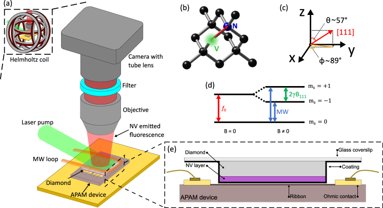
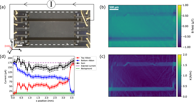
To perform wide-field magnetic imaging, we used a home-built fluorescence microscope (schematic shown in figure 1(a)) [33]. The diamond sensor, placed on top of the APAM device, was illuminated from the side with a 532 nm laser beam, with a laser power of 1.1 W. The laser beam was expanded with a 400 mm focal length lens in order to obtain a uniform illumination in the camera field of view (2.43.8 mm2). The NV fluorescence was collected by a 5x objective (0.13 numerical aperture) and filtered by a long-pass filter (650 nm cutoff wavelength) before being imaged trough a tube lens (f = 100 mm) onto a CMOS camera. The camera exposure time was set to 25 ms and a 44 pixel binning was applied to obtain an image of 250400 pixels with a pixel size of 9.5 m. The microscope was placed inside a 3-axis Helmholtz coil set, used to apply a static 1 mT bias magnetic field along the NV axis, defined as the [111] diamond crystallographic direction as shown in figure 1(b) and (c). The bias magnetic field lifts the degeneracy between the NV ground-state spin sublevels required to perform optically-detected magnetic resonance (ODMR) spectroscopy. The resonance frequencies of the [111] oriented NVs, as shown in figure 1(d), are shifted from the zero-field splitting GHz by , with kHz T-1 being the NV gyromagnetic ratio and the magnetic field along the NV axis. As the laser pumps NVs into the bright sublevel, we performed ODMR spectroscopy by applying a microwave (MW) field to drive transitions from the to the dark sublevels while monitoring the NV PL emission: when the MW is on resonance with the , the PL intensity is reduced. In our apparatus, a copper loop placed above the diamond provided the MW excitation. The MW signal was generated by a TPI-1002-A MW source, pulsed by a Mini-Circuits ZASWA-2-50DRA+, then amplified into the copper loop with a Mini-Circuits ZHL-16W-43-S+.
II.2 NV Diamond Sample
Our NV diamond sensor was a 440.5 mm3 electronic grade diamond (native nitrogen density 5 ppb), that was CVD overgrown with a 4 m-thick 12C-enriched diamond layer doped with 25 ppm of 14N on one surface (process performed by Applied Diamond, Inc). After overgrowth, it was irradiated with a 1 MeV energy, 1.2e18 cm-2 fluence electron beam and vacuum-annealed as in Ref. [37] to form a NV ensemble. Finally, the diamond was cleaned with triacid solution (1:1:1 sulfuric, nitric and perchloric acids) at 250 ∘C for 1 hour. To avoid photocarriers excitation in the imaged device, we glued the non-NV-containing diamond side to a glass coverslip with a UV-curing transparent glue. Both the diamond and the coverslip were then coated with a three-layer stack made of 5 nm of Ti (to improve adhesion), 150 nm of Ag (to reflect photons and prevent photocurrent excitation), and 150 nm of Al2O3 (to avoid contact shorting in the device) [38]. As shown in figure 1(e), our measurements were performed with the diamond placed on top of the device, with the NV surface facing down. As a demonstration of the importance of protecting the device under studying, results of magnetic imaging without the three-layer stack and the consequences on APAM device functioning are reported in the supplementary materials [39].
II.3 Characterization Techniques
SEM analysis was performed with a FEI Nanolab 650 microscope, operated in secondary electron mode with an acceleration voltage of keV and at a working distance of mm. Laser profilometry was done by using a Keyence VK-X150 microscope equipped with a 658 nm laser.
II.4 APAM Device
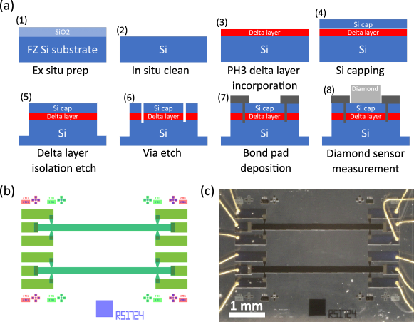
The schematic of the APAM device fabrication process is shown in figure 2(a). APAM phosphorus delta-doped layer devices were prepared on flash-cleaned float zone Si(100) substrates through UHV dosing with phosphine and subsequent encapsulation with 30 nm of low temperature epitaxial silicon. The samples were then processed using standard cleanroom procedures using an all-optical lithography approach. Two Hall bar structures were etched into the silicon substrate through a Bosch etch, taking care to etch deep enough (10 m) to isolate the delta layer from the surrounding silicon substrate. An ICP silicon etch was then used to etch several shallow vias through the APAM silicon cap to the APAM delta layer. Finally, electrical contact to the APAM delta layer was achieved by the addition of 300nm-thick Ti/Al bond pads using a standard metals liftoff process. More details on the APAM device fabrication process are reported in Ref. [6]. Figure 2(b) shows the schematic top view of the chip, whereas the final APAM device optical picture is shown in figure 2(c).
III Results and Discussion
III.1 Magnetic Field Measurements
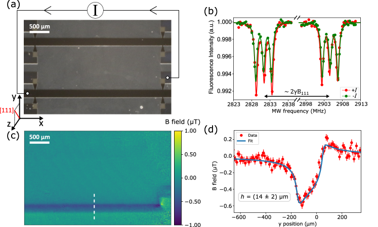
We injected a current of A (applied voltage of 1.9 V) through one of the APAM device ribbons, as shown in figure 3(a). We performed wide-field ODMR spectroscopy, collecting emitted NV PL while sweeping the MW frequency, obtaining an ODMR spectrum for each camera pixel. We then fit the ODMR spectra for each pixel, shown in figure 3(b), to determine the resonance frequencies. The frequency difference between the two resonance frequencies is used to calculate the value of the magnetic field along the NV axis for each pixel, allowing us to obtain a 2D magnetic field map. To isolate the contributions of the injected current to the magnetic field (and remove any background magnetic fields), we collected two wide-field magnetic image measurements, one with positive current , the other with a current of opposite sign . To improve the signal-to-noise ratio, each measurement was repeated and averaged 10 times for a total acquisition time of 3 h. The normalized difference of the two images was then calculated to remove the background magnetic field. The magnetic field map resulting from wide-field ODMR spectroscopy is displayed in figure 3(c).
III.2 Stand-off Distance Estimation
To estimate the stand-off distance between the NV-layer and the APAM device, we used the following equations for the magnetic field generated along a line-cut of an infinitely long 2D ribbon having width m and carrying a current [40]:
| (1) |
Here and are respectively the directions along the width of the ribbons and perpendicular to the device plane and mT/A. The magnetic field projection along the NV axis is given by:
| (2) |
with 89∘ and 57∘ being the two angles defining the NV-axis direction. and are respectively the angle from and the angle in the plane, defining the direction of the bias magnetic field aligned with the [111] diamond axis, as shown in figure 1(c).
Finally, the finite NV layer thickness m is taken into account by replacing with , and averaging over the interval [41]:
| (3) |
resulting in m, as shown in figure 3(d). The error bars on the experimental data in figure 3(d) come from the standard deviation (noise floor) of the magnetic fields measured over a line-cut away from the ribbon, i.e. where , resulting in T.
III.3 Current Reconstruction
After finding the stand-off distance, we reconstructed the surface current density from the single vector component magnetic field map . We assumed that the currents flowing in the APAM device are quasistatic and confined in a 2D sheet, and we used the inverted Biot-Savart law in Fourier space to obtain [42, 43, 44]:
| (4) |
Here and are respectively the current density components and the magnetic field map in Fourier space, and are the Fourier-space wave vector components, and is the NV axis orientation. The function is the Green’s function
| (5) |
which requires a window function to suppress the measurement white noise at high spatial frequencies when tends to zero. To achieve this, we use a Hann window function
| (6) |
with cutoff wave vector . Noise rejection of high values reduces the spatial resolution of the calculated current distribution (which is already limited by the stand-off distance), so is found empirically to adjust the trade-off between these two effects. Finally, the inverse Fourier transform of Eq. 4 leads to the current density components and as well as the current density magnitude .
III.4 Functioning APAM Device
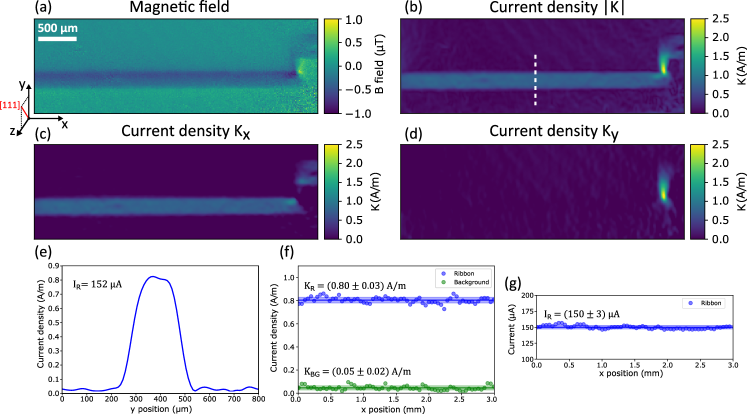
The reconstructed current density for the magnetic field map of figure 4(a) is shown in figure 4(b,c,d). To check the quality of the current reconstruction algorithm, we integrated the current density over the width of the ribbon to obtain a total current of A (figure 4(e)). The value of the surface current density in the ribbon as function of is shown in figure 4(f), resulting in a constant value of A/m. The resulting current obtained by integrating over the width of the ribbon is shown in figure 4(g). The constant value of A proves the current stability across the P-doped region and matches the nominal injected current of 150 A. The background surface current density measured in a region away from the ribbon is also shown in figure 4(f), showing a mean offset baseline of A/m and a standard deviation of A/m. The DC offset in the map is an artifact of the current reconstruction algorithm arising when is calculated from a single axis magnetic field measurement [44] while the standard deviation A/m represents the noise floor. gives a measurement of the surface current density sensitivity, leading to a smallest detectable current (i.e. current measured with a SNR = 1) in the 200 m wide ribbon of 6 A.
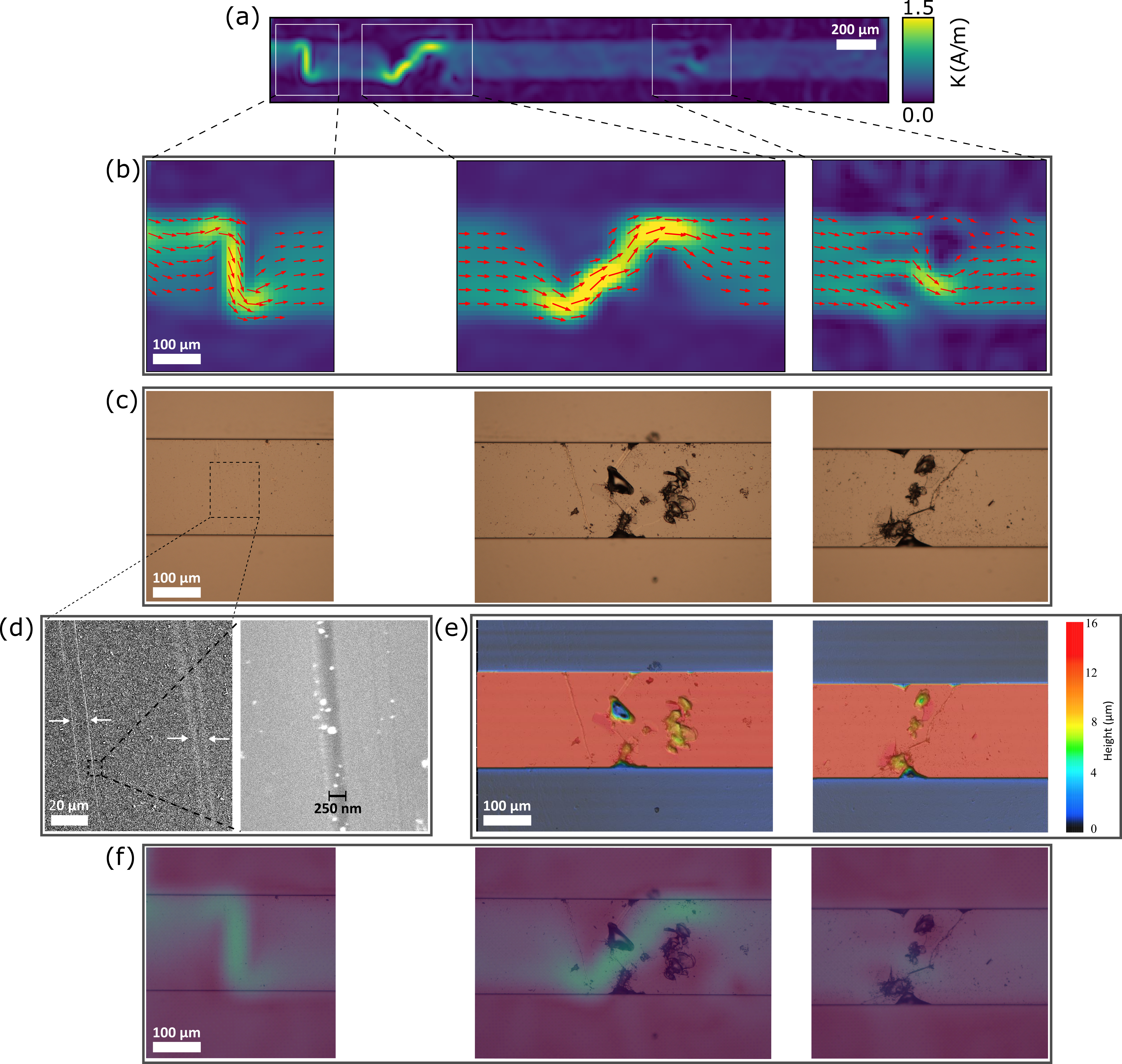
III.5 Faulty APAM Device
We can also detect failures in our APAM devices. An example is shown in figure 5(a) for an injected current of 150 A (applied voltage of 18 V), where there are sections of the ribbon for which we can observe impeded current flow. Figure 5(b) shows a zoom of the current path irregularities: the current direction around holes and choke points are indicated by the arrows, which have lengths proportional to the local current density magnitude. To asses the origins of these irregularities in the current flow, we compared the measured current density maps with optical images of the same areas (figure 5(c)), as well as SEM (figure 5(d)) and laser profilometry (figure 5(e)) analysis. From the set of optical images in figure 5(c) we could observe a correlation between current flow irregularities and material damage on the APAM device surface. SEM analysis on the left image of figure 5(d) shows the presence of two pairs of scratches each with lateral size of 250 nm, as shown in right panel of figure 5(d). We then used laser profilometry to obtain a 3D altitude image of the same areas. As seen in figure 5(e) some of the cracks on the device surface are several microns deep, enough to have removed the conductive P-doped region below Si surface. This allows us to attribute the current flow irregularities to the presence of material damage, such as cracks and scrapes. The overlay between current density maps and optical images, shown in figure 5(f), helps to see where the current is flowing around the device defects.
III.6 Current Leakage Between APAM structures
Finally, with the aim of detecting current leakage paths, we intentionally created leakages between the P-doped ribbons by connecting both of them to the current source, as shown in figure 6(a). By doing this, we expect the current to leave the bottom ribbon and flow through the Si substrate to reach the top one. Unsurprisingly, to inject a current of A we need to apply a voltage of 70 V, 10x higher than the previous cases, consistent with the current flowing through an undoped path. The resulting magnetic field map and reconstructed current density, reported in figure 6(b) and (c) respectively, show that the current is flowing in both ribbons. For a quantitative analysis we integrated the current density over the ribbons to calculate the current flowing along , with the result shown in figure 6(d). The error bars on the integrated current are calculated starting from the uncertainty on the measured magnetic field T, that is propagated through the current reconstruction algorithm to obtain A. We observed that the current profiles are consistent with the current being injected in the bottom ribbon and collected from the top one. Interestingly, the sum of the currents flowing in the two ribbons matches the total injected current only close to the injection and collection points, implying that there are leakage currents in between the ribbons that we do not detect. More quantitatively, the unobservable current, i.e. leakage current defined as the difference between the nominal injected current and total measured current (black curve in figure 6(d)), is at most 39 13 A. As the measured surface current density sensitivity is A/m (see figure 4(f)), the leak current to be detected with a SNR = 1 must flow in a sheet less than 1 mm wide. We postulate that we could not directly observe the current leakage path for several reasons. The first explanation is that the leakage path is three dimensional, making the current density reconstruction unreliable due to the 2D current density assumption of our model. The second explanation is that the leakage currents, no longer confined in the 2D P-doped regions, are spread over a wide area, resulting in a surface current density smaller than . Finally, if the leakage current behaves as a uniform sheet between the two ribbons, then its field would be largely along the direction (except at the edges), which is orthogonal to the NV sensing direction and would be largely invisible. Although the field from such a leakage current would be too weak to detect with the present apparatus, a follow-up experiment with an improved that measures the vector magnetic fields for each pixel may be able to detect it.
IV Conclusion
In summary, we have shown the capability to map the magnetic fields in an APAM device with micron-scale resolution over a millimeter-scale field of view area using NV wide-field magnetic imaging under ambient conditions without interfering with the operation of the device under study (see supplementary materials [39]). From the measured magnetic field maps, we reconstructed the surface current densities, leading to wide-field imaging of the current flowing in the device. That allowed us to obtain information on the APAM device properties and detect unexpected behavior, such as current path irregularities and leakages. Current density sensitivity is of order A/m, leading to a minimum detectable current of 6 A in the 200 m wide APAM ribbon. Further work will upgrade this experiment to detect and reconstruct 3D currents [45] as well as AC signals in the MHz or GHz range with appropriate NV manipulation techniques [46, 47]. The development of a NV-based diagnostic tool able to image where current is flowing and detect failures or leakages down to A/m could benefit the whole microelectronics community, with application not limited to APAM devices but extended to CMOS based technologies [48].
Acknowledgements
We thank George Burns, Michael Titze, and Edward Bielejec (Ion Beam Laboratory, Sandia National Laboratories) for help with diamond preparation. Sandia National Laboratories is a multi-mission laboratory managed and operated by National Technology and Engineering Solutions of Sandia, LLC, a wholly owned subsidiary of Honeywell International, Inc., for the DOE’s National Nuclear Security Administration under contract DE-NA0003525. This work was funded, in part, by the Laboratory Directed Research and Development Program and performed, in part, at the Center for Integrated Nanotechnologies, an Office of Science User Facility operated for the U.S. Department of Energy (DOE) Office of Science. This paper describes objective technical results and analysis. Any subjective views or opinions that might be expressed in the paper do not necessarily represent the views of the U.S. Department of Energy or the United States Government.
References
References
- Ruess et al. [2004] F. J. Ruess, L. Oberbeck, M. Y. Simmons, K. E. J. Goh, A. R. Hamilton, T. Hallam, S. R. Schofield, N. J. Curson, and R. G. Clark, “Toward atomic-scale device fabrication in silicon using scanning probe microscopy,” Nano Lett. 4, 1969–1973 (2004).
- Shen et al. [2004] T.-C. Shen, J. Kline, T. Schenkel, S. Robinson, J.-Y. Ji, C. Yang, R.-R. Du, and J. Tucker, “Nanoscale electronics based on two-dimensional dopant patterns in silicon,” J. Vac. Sci. Technol. B 22, 3182–3185 (2004).
- Simmons et al. [2005] M. Simmons, F. Ruess, K. Goh, T. Hallam, S. Schofield, L. Oberbeck, N. Curson, A. Hamilton, M. Butcher, R. Clark, et al., “Scanning probe microscopy for silicon device fabrication,” Mol. Simul. 31, 505–515 (2005).
- Rueß et al. [2007] F. J. Rueß, W. Pok, T. C. Reusch, M. J. Butcher, K. E. J. Goh, L. Oberbeck, G. Scappucci, A. R. Hamilton, and M. Y. Simmons, “Realization of atomically controlled dopant devices in silicon,” Small 3, 563–567 (2007).
- McKibbin et al. [2013] S. McKibbin, G. Scappucci, W. Pok, and M. Simmons, “Epitaxial top-gated atomic-scale silicon wire in a three-dimensional architecture,” Nanotechnology 24, 045303 (2013).
- Ward et al. [2017] D. R. Ward, M. T. Marshall, D. Campbell, T.-M. Lu, J. C. Koepke, D. A. Scrymgeour, E. Bussmann, and S. Misra, “All-optical lithography process for contacting nanometer precision donor devices,” Appl. Phys. Lett. 111, 193101 (2017).
- Škereň et al. [2018] T. Škereň, N. Pascher, A. Garnier, P. Reynaud, E. Rolland, A. Thuaire, D. Widmer, X. Jehl, and A. Fuhrer, “Cmos platform for atomic-scale device fabrication,” Nanotechnology 29, 435302 (2018).
- Ward et al. [2020] D. R. Ward, S. W. Schmucker, E. M. Anderson, E. Bussmann, L. Tracy, T.-M. Lu, L. N. Maurer, A. Baczewski, D. M. Campbell, M. T. Marshall, and S. Misra, “Atomic precision advanced manufacturing for digital electronics,” Electronic Device Failure Analysis 22, 4–11 (2020).
- Bussmann et al. [2021] E. Bussmann, R. E. Butera, J. H. Owen, J. N. Randall, S. M. Rinaldi, A. D. Baczewski, and S. Misra, “Atomic-precision advanced manufacturing for si quantum computing,” MRS Bulletin 46, 607–615 (2021).
- Weber et al. [2012] B. Weber, S. Mahapatra, H. Ryu, S. Lee, A. Fuhrer, T. Reusch, D. Thompson, W. Lee, G. Klimeck, L. C. Hollenberg, et al., “Ohm’s law survives to the atomic scale,” Science 335, 64–67 (2012).
- Fuhrer et al. [2009] A. Fuhrer, M. Fuchsle, T. Reusch, B. Weber, and M. Simmons, “Atomic-scale, all epitaxial in-plane gated donor quantum dot in silicon,” Nano Lett. 9, 707–710 (2009).
- Fuechsle et al. [2012] M. Fuechsle, J. A. Miwa, S. Mahapatra, H. Ryu, S. Lee, O. Warschkow, L. C. Hollenberg, G. Klimeck, and M. Y. Simmons, “A single-atom transistor,” Nat. Nanotechnol. 7, 242–246 (2012).
- He et al. [2019] Y. He, S. Gorman, D. Keith, L. Kranz, J. Keizer, and M. Simmons, “A two-qubit gate between phosphorus donor electrons in silicon,” Nature 571, 371–375 (2019).
- Wang et al. [2020] X. Wang, J. Wyrick, R. V. Kashid, P. Namboodiri, S. W. Schmucker, A. Murphy, M. D. Stewart, and R. M. Silver, “Atomic-scale control of tunneling in donor-based devices,” Commun. Phys. 3, 1–9 (2020).
- Škereň et al. [2020] T. Škereň, S. A. Köster, B. Douhard, C. Fleischmann, and A. Fuhrer, “Bipolar device fabrication using a scanning tunnelling microscope,” Nature Electronics , 1–7 (2020).
- Wang et al. [2021] X. Wang, E. Khatami, F. Fei, J. Wyrick, P. Namboodiri, R. Kashid, A. F. Rigosi, G. Bryant, and R. Silver, “Quantum simulation of an extended fermi-hubbard model using a 2d lattice of dopant-based quantum dots,” arXiv preprint arXiv:2110.08982 (2021).
- Gao et al. [2020] X. Gao, L. A. Tracy, E. M. Anderson, D. M. Campbell, J. A. Ivie, T.-M. Lu, D. Mamaluy, S. W. Schmucker, and S. Misra, “Modeling assisted room temperature operation of atomic precision advanced manufacturing devices,” 2020 International Conference on Simulation of Semiconductor Processes and Devices (SISPAD) , 277–280 (2020).
- Lu et al. [2021] T.-M. Lu, X. Gao, E. M. Anderson, J. P. Mendez, D. M. Campbell, J. A. Ivie, S. W. Schmucker, A. Grine, P. Lu, L. A. Tracy, R. Arghavani, and S. Misra, “Path towards a vertical tfet enabled by atomic precision advanced manufacturing,” 2021 Silicon Nanoelectronics Workshop (SNW) , 1–2 (2021).
- Mamaluy et al. [2021] D. Mamaluy, J. P. Mendez, X. Gao, and S. Misra, “Revealing quantum effects in highly conductive -layer systems,” Commun. Phys. 4 (2021).
- Bussmann et al. [2015] E. Bussmann, M. Rudolph, G. Subramania, S. Misra, S. Carr, E. Langlois, J. Dominguez, T. Pluym, M. Lilly, and M. Carroll, “Scanning capacitance microscopy registration of buried atomic-precision donor devices,” Nanotechnology 26, 085701 (2015).
- Scrymgeour et al. [2017] D. Scrymgeour, A. Baca, K. Fishgrab, R. Simonson, M. Marshall, E. Bussmann, C. Nakakura, M. Anderson, and S. Misra, “Determining the resolution of scanning microwave impedance microscopy using atomic-precision buried donor structures,” Appl. Surf. Sci.s 423, 1097–1102 (2017).
- Gramse et al. [2017] G. Gramse, A. Kölker, T. Lim, T. J. Stock, H. Solanki, S. R. Schofield, E. Brinciotti, G. Aeppli, F. Kienberger, and N. J. Curson, “Nondestructive imaging of atomically thin nanostructures buried in silicon,” Science Advances 3, e1602586 (2017).
- Katzenmeyer et al. [2020] A. M. Katzenmeyer, T. S. Luk, E. Bussmann, S. Young, E. M. Anderson, M. T. Marshall, J. A. Ohlhausen, P. Kotula, P. Lu, D. M. Campbell, et al., “Assessing atomically thin delta-doping of silicon using mid-infrared ellipsometry,” J. Mater. Res. 35, 2098–2105 (2020).
- Gramse et al. [2020] G. Gramse, A. Koelker, T. Škereň, T. J. Stock, G. Aeppli, F. Kienberger, A. Fuhrer, and N. J. Curson, “Nanoscale imaging of mobile carriers and trapped charges in delta doped silicon p–n junctions,” Nat. Electron. 3, 531–538 (2020).
- Kölker et al. [2022] A. Kölker, G. Gramse, T. J. Stock, G. Aeppli, and N. J. Curson, “In operando charge transport imaging of atomically thin dopant nanostructures in silicon,” Nanoscale 14, 6437–6448 (2022).
- Oberbeck et al. [2002] L. Oberbeck, N. Curson, M. Simmons, R. Brenner, A. Hamilton, S. Schofield, and R. Clark, “Encapsulation of phosphorus dopants in silicon for the fabrication of a quantum computer,” Appl. Phys. Lett. 81, 3197–3199 (2002).
- Hagmann et al. [2018] J. A. Hagmann, X. Wang, P. Namboodiri, J. Wyrick, R. Murray, M. Stewart Jr, R. M. Silver, and C. A. Richter, “High resolution thickness measurements of ultrathin si: P monolayers using weak localization,” Appl. Phys. Lett. 112, 043102 (2018).
- Doherty et al. [2013] M. W. Doherty, N. B. Manson, P. Delaney, F. Jelezko, J. Wrachtrup, and L. Hollenberg, “The nitrogen-vacancy colour centre in diamond,” Physics Reports 528, 1–45 (2013).
- Rondin et al. [2014] L. Rondin, J.-P. Tetienne, T. Hingan, J.-F. Roch, P. Maletinsky, and V. Jacques, “Magnetometry with nitrogen-vacancy defects in diamond,” Rep. Prog. Phys. 77, 056503 (2014).
- Chipaux et al. [2015] M. Chipaux, A. Tallaire, J. Achard, S. Pezzagna, J. Meijer, V. Jacques, J.-F. Roch, and T. Debuisschert, “Magnetic imaging with an ensemble of nitrogen-vacancy centers in diamond,” Eur. Phys. J. D 69, 166 (2015).
- Kehayias et al. [2020] P. Kehayias, E. Bussmann, T. M. Lu, and A. M. Mounce, “A physically unclonable function using nv diamond magnetometry and micromagnet arrays,” J. Appl. Phys. 127, 203904 (2020).
- Glenn et al. [2017] D. R. Glenn, R. R. Fu, P. Kehayias, D. Le Sage, E. A. Lima, B. P. Weiss, and R. L. Walsworth, “Micrometer-scale magnetic imaging of geological samples using a quantum diamond microscope,” Geochem. Geophys., Geosyst. 18, 3254–3267 (2017).
- Levine et al. [2019] E. V. Levine, M. J. Turner, P. Kehayias, C. A. Hart, N. Langellier, R. Trubko, D. R. Glenn, R. R. Fu, and R. L. Walsworth, “Principles and techniques of the quantum diamond microscope,” Nanophotonics 8, 1945–1973 (2019).
- Jalilian et al. [2011] R. Jalilian, L. A. Jauregui, G. Lopez, J. Tian, C. Roecker, M. M. Yazdanpanah, R. W. Cohn, I. Jovanovic, and Y. Chen, “Scanning gate microscopy on graphene: charge inhomogeneity and extrinsic doping,” Nanotechnology 22, 295705 (2011).
- Felt [2005] F. S. Felt, “Analysis of a microcircuit failure using SQUID and MR current imaging,” International Symposium for Testing and Failure Analysis (ISTFA) , 169–177 (2005).
- Pu, Thomson, and Bridges [2009] A. Pu, D. Thomson, and G. Bridges, “Location of current carrying failure sites in integrated circuits by magnetic force microscopy at large probe-to-sample separation,” Microelectronic Engineering 86, 16–23 (2009).
- Henshaw et al. [2022] J. Henshaw, P. Kehayias, M. S. Ziabari, M. Titze, E. Morissette, K. Watanabe, T. Taniguchi, J. I. A. Li, V. M. Acosta, E. Bielejec, M. P. Lilly, and A. M. Mounce, “Nanoscale solid-state nuclear quadrupole resonance spectroscopy using depth-optimized nitrogen-vacancy ensembles in diamond,” Appl. Phys. Lett. 120, 174002 (2022).
- Kehayias et al. [2022] P. Kehayias, E. V. Levine, L. Basso, J. Henshaw, M. Saleh Ziabari, M. Titze, R. Haltli, J. Okoro, D. R. Tibbetts, D. M. Udoni, E. Bielejec, M. P. Lilly, T.-M. Lu, P. D. D. Schwindt, and A. M. Mounce, “Measurement and simulation of the magnetic fields from a 555 timer integrated circuit using a quantum diamond microscope and finite-element analysis,” Phys. Rev. Applied 17, 014021 (2022).
- [39] “See supplemental material.” .
- Hingant et al. [2015] T. Hingant, J.-P. Tetienne, L. J. Martínez, K. Garcia, D. Ravelosona, J.-F. Roch, and V. Jacques, “Measuring the magnetic moment density in patterned ultrathin ferromagnets with submicrometer resolution,” Phys. Rev. Applied 4, 014003 (2015).
- Abrahams et al. [2021] G. J. Abrahams, S. C. Scholten, A. J. Healey, I. O. Robertson, N. Dontschuk, S. Q. Lim, B. C. Johnson, D. A. Simpson, L. C. L. Hollenberg, and J.-P. Tetienne, “An integrated widefield probe for practical diamond nitrogen-vacancy microscopy,” Appl. Phys. Lett. 119, 254002 (2021).
- Roth, Sepulveda, and Wikswo [1989] B. J. Roth, N. G. Sepulveda, and J. P. Wikswo, “Using a magnetometer to image a two‐dimensional current distribution,” J. Appl. Phys. 65, 361–372 (1989).
- Chang et al. [2017] K. Chang, A. Eichler, J. Rhensius, L. Lorenzelli, and C. L. Degen, “Nanoscale imaging of current density with a single-spin magnetometer,” Nano Letters 17, 2367–2373 (2017).
- Broadway et al. [2020] D. Broadway, S. Lillie, S. Scholten, D. Rohner, N. Dontschuk, P. Maletinsky, J.-P. Tetienne, and L. Hollenberg, “Improved current density and magnetization reconstruction through vector magnetic field measurements,” Phys. Rev. Applied 14, 024076 (2020).
- Oliver et al. [2022] S. M. Oliver, D. J. Martynowych, M. J. Turner, D. A. Hopper, R. L. Walsworth, and E. V. Levine, “Vector magnetic current imaging of an 8 nm process node chip and 3d current distributions using the quantum diamond microscope,” arXiv:2202.08135 (2022).
- Horsley et al. [2018] A. Horsley, P. Appel, J. Wolters, J. Achard, A. Tallaire, P. Maletinsky, and P. Treutlein, “Microwave device characterization using a widefield diamond microscope,” Phys. Rev. Applied 10, 044039 (2018).
- Taylor et al. [2008] J. M. Taylor, P. Cappellaro, L. Childress, L. Jiang, D. Budker, P. R. Hemmer, A. Yacoby, R. Walsworth, and M. D. Lukin, “High-sensitivity diamond magnetometer with nanoscale resolution,” Nat. Phys. 4, 810–816 (2008).
- Turner et al. [2020] M. J. Turner, N. Langellier, R. Bainbridge, D. Walters, S. Meesala, T. M. Babinec, P. Kehayias, A. Yacoby, E. Hu, M. Lončar, R. L. Walsworth, and E. V. Levine, “Magnetic field fingerprinting of integrated-circuit activity with a quantum diamond microscope,” Phys. Rev. Applied 14, 014097 (2020).