Exciton localization on p-i-n junctions in two-dimensional crystals
Abstract
We consider a neutral exciton localized on a model p-i-n junction defined in a two-dimensional crystal: MoSe2 and phosphorene, using a variational approach to the effective mass Hamiltonian. The variational solution to the problem with non-separable center of mass provides the exciton density in the real space and accounts for the kinetic energy due to the exciton localization. For low values of the potential step across the junction, the exciton occupies an area which is much larger than the nominal width of the junction. Localization of the exciton within the junction area is accompanied by the appearance of the dipole moment induced by the local electric field. The induced dipole moment becomes a linear function of the potential step only when the step is sufficiently large. In consequence, the energy dependence on the step value is non-parabolic. We demonstrate that the exciton gets localized not exactly at the center of the junction but on the side which is more energetically favourable for the heavier carrier: electron or hole.
I Introduction
Reduction of dimensionality and large carrier effective masses in monolayer transition-metal dichalcogenide tmdc1 ; tmdc3 and phosphorene xia ; castelano result in large exciton binding energies tran ; seixas ; kep3 ; varga ; starkchav ; starkchav2 ; peeters ; rodin exceeding by two orders of magnitude the corresponding values in bulk semiconductors. Large binding energy allows for tuning the exciton line in the luminescent spectrum by the Stark effect induced by an in-plane electric field starkchav which leads to a red-shift of the electron-hole recombination energy due to the interaction of the intrinsic or induced exciton dipole moment with the field. The Stark effect was studied for states in quantum wells qw0 ; qw1 or quantum dots qd0 ; qd1 ; qd2 ; qd3 where the quantum confinement stabilized the weakly bound exciton against dissociation by the electric field. Conversely, the Stark effect for strongly bound excitons in a transition metal dichalcogenide has recently been used to trap the excitons on the electric field at the p-i-n junction na .
The purpose of the present work is to describe the exciton confinement in a model of the p-i-n junction by a numerical albeit exact solution of the two-particle problem. The trapping mechanism was explained na as due to an effective potential for the exciton that contains a term due to the electric field , where is the electric field at the junction and is the polarizability of the exciton, which for the homogeneous electric field can be determined by the solution of the electron-hole problem in the relative electron-hole coordinates na ; starkchav ; starkchav2 . The electric field in the junction na is not homogeneous and the motion of the center of mass of the exciton does not separate from the eigenproblem in the relative coordinates. Therefore, the center of mass requires treatment on equal rights with the relative electron-hole coordinates which we provide in this work. The solution accounts for the kinetic energy due to the exciton confinement at the junction and provides information on the exciton localization: its mean position and extent of its wave function in the real space. We find that the range of exciton confinement depends strongly on the value of the potential step at the junction, and for a low value of the step the confinement range can largely exceed the nominal width of the junction. Then, the wave function is present in a region with a widely changing electric field that makes the homogeneous field solution not directly adequate to a local field case. In particular, the electric field at the center of the junction is a linear function of the potential step at the junction, but the induced dipole moment is not and the reaction of the exciton energy on the step is not parabolic as for Stark effect in the homogenous electric field.
II Theory
We work with the effective band Hamiltonian for the electron-hole pair at the junction
| (1) | |||||
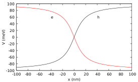
with standing for the electron or hole mass along the or directions. We use the model potential of the p-i-n junction in the form where defines the scale of the potential step along the junction and the variation rate is given by . The model potential is plotted in Fig. 1 for the electron (, red line) and the hole (, black line). The potential pushes the non-interacting carriers away from the junction center. In Eq. (1) is the effective 2D interaction given by the Keldysh potential kep1 ; na ; kep2 ; kep3 ; varga ; ansatz ; starkchav ; starkchav2 ; peeters ; rodin ,
| (2) |
where and are the Struve and Bessel functions of the second kind, is the screening length that is a measure of the polarizability of the 2D semiconductor and is the dielectric constant. At large electron-hole distances the interaction potential tends to the 3D Coulomb form . At small electron-hole distances , acquires a logarithmic singularity of the 2D Coulomb potential. For evaluation of the interaction potential we use the method of Ref. ansatz . The intrinsic area where the exciton confinement occurs in the experiment na has a length of several dozens of nanometers. Here we discuss the results with the parameter ranging from 15 to 60nm. The variation of the potential by and occurs at lengths of and , respectively. In the experimental situation na the carriers are additionally confined by the space-charge density outside the intrinsic region. Here we assume that the depletion region is arbitrarily wide for a description of the exciton binding purely on the local electric field.
Using the center-of-mass coordinates , , with , and the relative electron-hole coordinates and , the Hamiltonian is written as
| (3) | |||||
with the reduces masses and . The motion of the center of mass along the junction separates from the rest of the coordinates, and we assume that the wave function over has the form of a plane wave with a zero wave vector. For a constant electric field oriented along the direction, studied for the discussion of the Stark effect starkchav ; starkchav2 ; na , the center of mass coordinate also separates, but this is not the case for the present problem with the non-linear potential of the junction .
The exciton states are determined using a variational approach varga with Gaussian basis
| (4) | |||
where are the linear variational coordinates determined by solving the generalized eigenvalue problem , with the matrix elements and . The centers of the Gaussian are distributed on a 3D mesh with , and , with , and being integers ranging from do . The values of select the region in space to be described by the variational wave function. The spacings ’s and the localization parameters of the Gaussian and are determined as nonlinear variational parameters by minimization of the energy estimate. Separate parameters for and are needed for phosphorene with its strongly anisotropic effective masses jakies ; 34 but also for the case of isotropic effective masses applied for MoSe2 due to the external potential acting only in the direction. The following results are obtained for , i.e. 17 Gaussians describing the wave function in each coordinate, i.e. for the total number of Gaussian functions used in the basis. The basis (4) is flexible enough to account for both the bound excitons and dissociated electron-hole pairs.
|
|
|
|
|
|

|
|
|
|
|
|
|
|

|
|
|
|
III Results and discussion
III.1 MoSe2
We first consider the material where the exciton trapping at the junction was accomplished na , MoSe2, the transition-metal dichalcogenide for which an isotropic effective mass model can be adopted with na ; cos and na ; cos2 . We take the dielectric constant and the screening length nm after Ref. na .
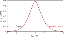
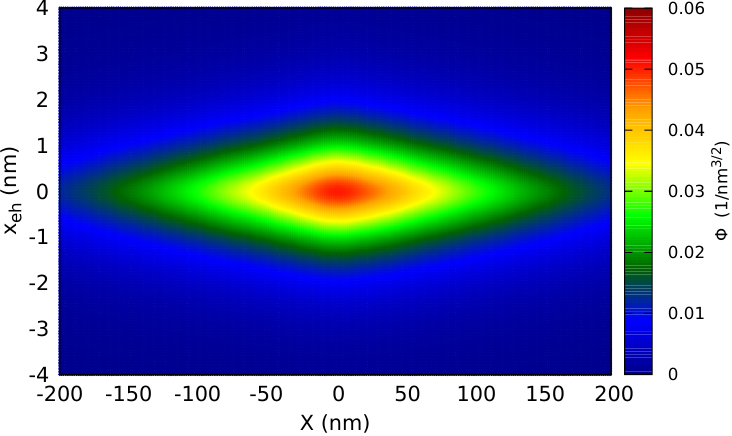
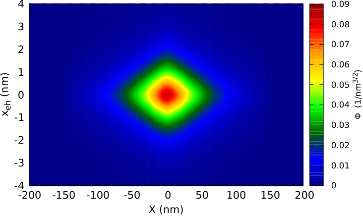
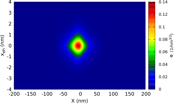
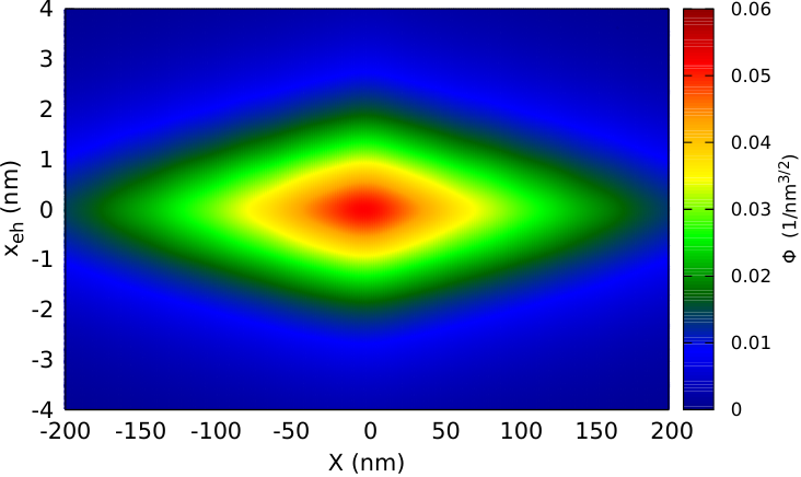
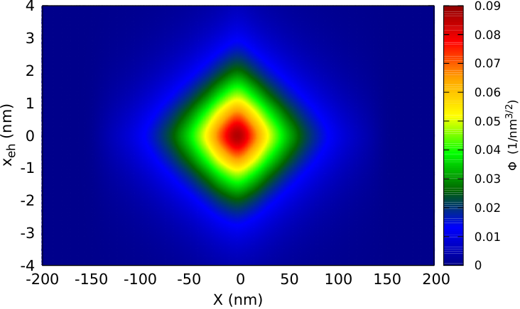
Figure 1(b) shows the lowest bound exciton state density calculated as for nm. The exciton is localized near the area where the potential gradient is maximal, and the exciton localization increases with . The center of the exciton is localized off the center of the junction on the side of the junction where the heavier carrier – here the electron – has a lower potential energy (see below). Figure 1(c) shows the density over the horizontal electron-hole distance . The potential of the considered range produces only a small shift of the density to a more positive , with the electron shifted to a more positive and the hole to a more negative position. The electron and hole densities calculated from the total wave function (not shown) are nearly identical to the exciton density due to the large extent of and the relative strong localization of the pair.
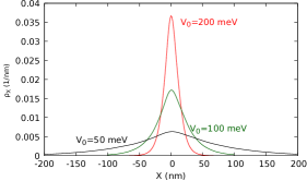
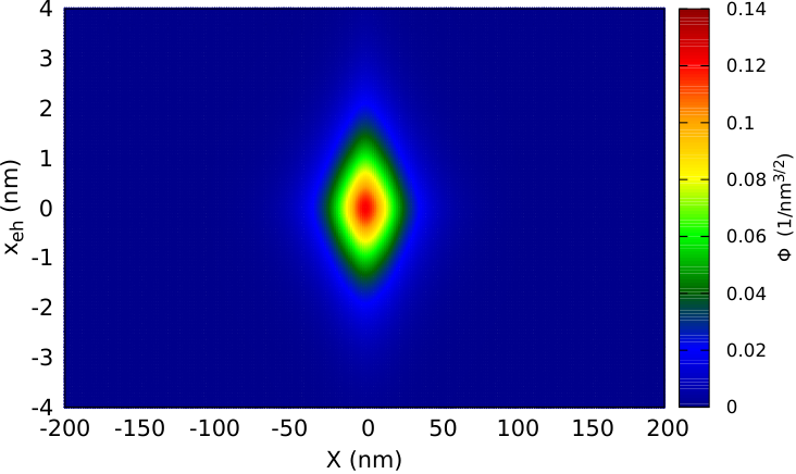
Figure 2 displays the cross section of the lowest energy bound electron-hole wave function taken at for meV, 100 meV and 200 meV. The range of the localization changes radically with only in the coordinate and not in .
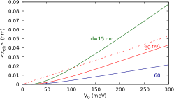
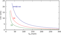
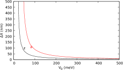
The process of exciton localization at the junction is illustrated in Fig. 3 where we considered several junction width parameters . The energy decrease with in Fig. 3(a) is a signature of the carrier separation by the electric field which, as we find, does not start at zero (Fig. 3(a)). The exciton localization in the region of a large electric field is associated with the cost of additional kinetic energy. For larger values of the electric field at the junction is lower, but the extent of exciton localization at the junction is decreased. The energy shift in the homogenous electric field falls with the square of the field starkchav ; starkchav2 which for the present potential implies a dependence while the exciton confinement energy depends on the localization as . The two effects seem to cancel each other out in the constant energy range of small . We observe that a nonzero value of the potential step is necessary to induce a significant dipole moment (Fig. 3(b)). As non-zero is introduced the range of exciton localization (Fig. 3(c)) becomes finite. However, for low most of the exciton stays outside of the action range of the local electric field (potential gradient) at the junction. For all studied values, the exciton size in terms of becomes equal to double the width parameter for meV. Only once the exciton is localized at the junction does the electron-hole system energy start to decrease visibly.
For comparison in Fig. 3(a) and (b) we plotted with the dashed red line the results for the homogenous electric field, i.e. for the potential of the junction replaced by its linear approximation: , for nm. For potential the dipole moment grows linearly with [Fig. 3(b)] starting from . The linear dependence of the dipole moment via its interaction with the field produces the parabolic dependence (the dashed line in Fig. 3(a)). For the junction potential , the growth of the dipole moment with follows after a delay. For all considered the dipole moment starts to grow for meV and becomes a linear function of only above 100 meV.
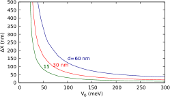
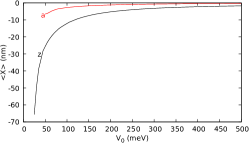
Figure 3(d) shows that the center of mass of the exciton approaches the center of the junction only in the limit, and for finite it stays on the positive side of the center of the junction. We return to this point for phosphorene, where the effect is more pronounced.
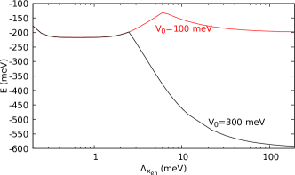
The ground-state energy meV obtained at (Ref. na indicates -217 meV) implies that the dissociated electron-hole pair appears in the ground state for . For above the bound hole-pair is not the ground state of the system, similarly to the studies of the Stark effect for a nonzero homogeneous electric field na ; starkchav ; starkchav2 . The applied basis resolves two separate minima for the bound and dissociated exciton. The results of the Hamiltonian diagonalization as a function of are given in Fig. 4, with the lower energy state corresponding to the bound exciton or the dissociated pair for meV and 300 meV, respectively. Here, we discuss only the properties of the bound electron-hole state for both below or above the dissociation threshold. The gradient minimalization method applied for optimization of the non-linear variational parameters tends to the closest energy minimum, so one can choose between the dissociated or bound exciton states.
III.2 phosphorene
The effective masses in phosphorene exhibit strong anisotropy with larger (smaller) values in the zigzag (armchair) crystal direction jakies ; 34 . For monolayer black phosphorous, we adopted the values of effective masses derived by fitting the results of the single-band approximation to the results of the atomistic tight-binding tb modelling for the harmonic oscillator confinement potential of Ref. szafran . That is, we take , for the electron masses in the armchair and zigzag directions szafran , respectively. For hole we take for the armchair direction szafran . The hole mass in the zigzag direction was not adopted from Ref. szafran but set to . The literature values for the zigzag mass of the hole vary from 34 ; 43 to 48 or 47 . The selected choice of the effective masses provides the electron-hole pair reduced masses that agree with the ones given in Table 2 of Ref. castelano for monolayer phosphorene. For the interaction potential we take the screening length of nm and the effective dielectric constant of after Supporting Information to Ref. castelano .
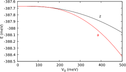
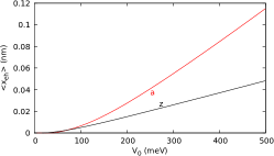
In calculations for phosphorene we fix the junction width parameter to nm. We keep the junction potential variation along the axis that we align with either armchair or zigzag crystal direction. The reaction of the exciton energy to the external potential is prompter for the junction defined along the armchair direction (Fig. 5(a)), and the induced dipole moment [Fig. 5(b)] is also larger in this direction where the masses are lighter. This finding is consistent with the conclusions of Ref. starkchav for the case of a homogeneous electric field in phosphorene.
The cross sections of the wave function for is plotted in Fig. 6 for the zigzag (a,b) and armchair (c,d) orientation of the wave function. The orientation of the junction has a pronounced effect on the exciton localization along the axis with the total mass for the armchair orientation for the junction defined along the zigzag crystal direction. The reduced mass in the direction is for the armchair and for the zigzag orientation, hence the varied localization along the vertical axis of Fig. 6. Fig. 5(c) indicates that the width of the exciton wave function becomes equal to for meV ( meV) for the junction defined along the zigzag (armchair) direction.
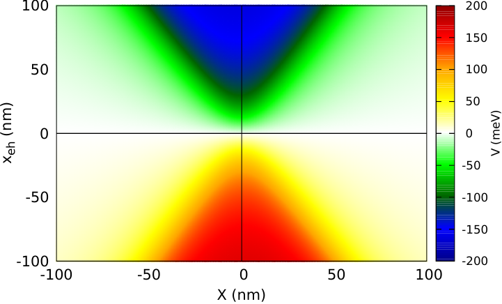
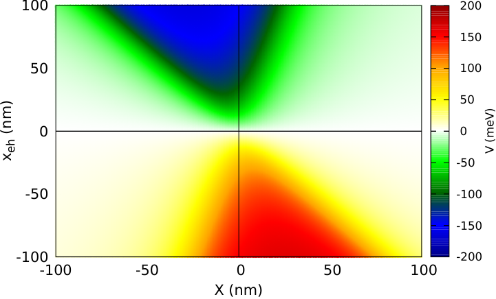
For phosphorene, the center of the exciton density is shifted to the left of the junction center [Fig. 6 and Fig. 5(d)]. The shift is smaller for the armchair orientation of the junction [Fig. 6(c,d)] and large for the zigzag-oriented junction [Fig. 6(a,b) and Fig. 5(d)]. As a general rule, the shift is large when one of the carriers is much heavier than the other and the shift appears in the direction of lower potential energy in the potential for the heavier carrier. In the results for MoSe2 (precedent subsection), the shift was observed to the positive side of the junction and the electron was slightly heavier. For phosphorene, the hole is heavier and the center of mass is shifted to the negative side of the junction. For the zigzag orientation, the mass difference is very pronounced; hence, the strong shift, much larger than the average electron-hole distance. The shift is directly related to the potential landscape at the junction. In Fig. 7 we plotted the external potential for both carriers, i.e. on the (, plane. The anisotropy of the masses translates to a shift of the potential minimum to the negative side of , which produces the pronounced asymmetry for the zigzag orientation of the junction. The interaction potential of Hamiltonian (3) is independent of and creates a valley along of depth that depends on . The displacement of the wave function to positive is not very pronounced (see Fig. 6 and Fig. 5(b)) since the strong interaction potential keeps the carriers close to one another. Instead, the wave function is shifted to the negative side of the junction where the minimum of the potential landscape is closer to the axis. The effect is particularly well seen in Fig. 6(a,b) (see also Fig. 5(d)). Note that for a homogeneous electric field, only the reduced masses and not the separate masses of the electron and hole matter for the properties of the bound exciton states starkchav .
|
|
IV Summary and Conclusions
We have studied bound electron-hole pairs at a p-i-n junction defined within a two-dimensional crystal using a model with a finite spatial range and potential step across the junction with the electric field in the center of the junction proportional to . The problem was solved with a variational calculation using the basis of Gaussians centered on a grid spanned by the relative coordinates of the carriers and the center of mass, which is not separable in the inhomogeneous electric field. The appearance of the dipole moment induced by the local electric field at the junction is accompanied by a build-up of the exciton kinetic energy as a result of the localization at the junction. The compensation of the two contributions leads to a range of values of the potential step of the junction that has a negligible influence on the exciton energy. For MoSe2 and phosphorene, localization of the exciton wave function in a range comparable with the junction length requires a potential difference across the junction of the order of meV. For lower values, the carriers occupy the region in space where the electric field is much smaller than at the center of the junction. The induced dipole moment dependence on the potential step deviates from linear, which is expected for the Stark effect in a homogenous electric field. In consequence, the exciton energy is not a parabolic function of . We have demonstrated that the localized exciton is shifted off the center of the junction in the direction in which the junction potential energy for the heavier carrier is lower.
Acknowledgments
Calculations for this work were performed on the PL-GRID infrastructure.
References
- (1) Q. H. Wang, K. Kalantar-Zadeh, A. Kis, J. N. Coleman, and M. S. Strano, Nat. Nanotechnol. 7, 699 (2012).
- (2) A. K. Geim and I. V. Grigorieva, Nature (London) 499, 419 (2013).
- (3) F. Xia, H. Wang, and Y. Jia, Nat. Commun. 5, 4458 (2014).
- (4) A.Castellanos-Gomez, L. Vicarelli, E. Prada, J.O. Island, K. L. Narasimha-Acharya, S. I Blanter, D. J. Groenendijk, M. Buscema, G.A. Steele, J. V. Alvarez, H. W. Zandbergen, J.J. Palacios, and H.S.J. van der Zant, 2D Materials 1, 025001 (2014).
- (5) V. Tran, R. Soklaski, Y. Liand, and L. Yang, Phys. Rev. B 89, 235319 (2014).
- (6) L. Seixas, A. S. Rodin, A. Carvalho, and A. H. Castro Neto, Phys. Rev. B 91, 115437 (2015).
- (7) D.V. Tuan, M. Yang, and H. Dery, Phys. Rev. B 98, 125308 (2018).
- (8) D.W. Kidd, D.K. Zhang, and K. Varga, Phys. Rev. B 93, 125423 (2016).
- (9) A. Chaves, T.Low, P. Avouris, D. Cakir, and F.M. Peeters, Phys. Rev. B 91, 155311 (2015).
- (10) L. S. R. Cavalcante, D. R. da Costa, G. A. Farias, D. R. Reichman, and A. Chaves, Phys. Rev. B 98, 245309 (2018).
- (11) A.S. Rodin, A. Carvalho, and A.H. Castro Neto, Phys. Rev. B 90, 075429 (2014).
- (12) M. Van der Donck and F.M. Peeters, Phys. Rev. B 98, 235401 (2018).
- (13) D. A. B. Miller, D. S. Chemla, T. C. Damen, A. C. Gossard, W. Wiegmann, T. H. Wood, and C. A. Burrus Phys. Rev. Lett. 53, 2173 (1984).
- (14) Y.-H. Kuo, Y.K. Lee, Y. Ge, S. Ren, J. E. Roth, T.I. Kamins, D.A.B Miller, J.S. Harris, Nature. 437 1334 (2005).
- (15) P. W. Fry, I. E. Itskevich, D. J. Mowbray, M. S. Skolnick, J. J. Finley, J. A. Barker, E. P. O’Reilly, L. R. Wilson, I. A. Larkin, P. A. Maksym, M. Hopkinson, M. Al-Khafaji, J. P. R. David, A. G. Cullis, G. Hill, and J. C. Clark Phys. Rev. Lett. 84, 733 (2000).
- (16) W. Sheng and J.-P. Leburton, Phys. Rev. Lett. 88, 167401 (2002).
- (17) K. L. Janssens, B. Partoens, and F. M. Peeters, Phys. Rev. B 65, 233301 (2002)
- (18) H. J. Krenner, M. Sabathil, E. C. Clark, A. F. Kress, D. Schuh, M. Bichler, G. Abstreiter, and J. J. Finley, Phys. Rev. Lett. 94, 057402 (2005).
- (19) D. Thureja, A. Imamoglu, T. Smolenski, I. Amelio, A. Popert, T. Chervy, L. Xiaobo, L. Song, K. Barmak, K. Watanabe, T. Taniguchi, D.J. Norris, M. Kroner, and P. A. Murthy, Nature 606, 298 (2022).
- (20) L. V. Keldysh, JETP Lett. 29, 658 (1979).
- (21) O.L. Berman and R.Y Kezarshvili, Phys. Rev. B 96, 094502 (2017).
- (22) P. Cudazzo, I.V. Tokatly, and A. Rubio, Phys. Rev. B 84, 085406 (2011).
- (23) M. Akhar, G. Anderson, R. Zhao, A. Alruqi, J. E. Mroczkowska, G. Sumanasekera, and J. B. Jasinski, npj 2D Mater. Appl. 1, 5 (2017).
- (24) J. Qiao, X. Kong, Z. X. Hu, F. Yang, and W. Ji, Nat. Commun. 5, 4475 (2014).
- (25) S. Larentis, H.C.P. Movva, B. Fallahazad, K. Kim, A. Behroozi, T. Taniguchi, K. Watanabe, S.K. Banerjee, and E. Tutu, Phys. Rev. B 97, 201407 (2018).
- (26) Y.Zhang, T.-R. Chang, B. Zhou, Y.-T. Cui, H. Yan, Z. Liu, F. Schmitt, J. Lee, R. Moore, Y. Chen, H. Lin, H.-T. Jeng, S.-K. Mo, Z. Hussain, A. Bansil, and Z.-X. Shen, Nature Nanotech 9, 111 (2014).
- (27) A. N. Rudenko and M. I. Katsnelson, Phys. Rev. B 89, 201408(R) (2014).
- (28) B. Szafran, Phys. Rev. B 101, 235313 (2020).
- (29) J. M. Pereira, Jr. and M. I. Katsnelson, Landau levels of single-layer and bilayer phosphorene, Phys. Rev. B 92, 075437 (2015).
- (30) X. Peng, Q. Wei, and A. Copple, Phys. Rev. B 90, 085402 (2014).
- (31) B. Sa, Y.-L. Li, Z. Sun, J. Qi, C. Wen, and B. Wu, Nanotechnology 26, 215205 (2015).