Self-Managing DRAM: A Low-Cost Framework for
Enabling Autonomous and Efficient in-DRAM Operations
Abstract
The memory controller is in charge of managing DRAM maintenance operations (e.g., refresh, RowHammer protection, memory scrubbing) in current DRAM chips. Implementing new maintenance operations often necessitates modifications in the DRAM interface, memory controller, and potentially other system components. Such modifications are only possible with a new DRAM standard, which takes a long time to develop, leading to slow progress in DRAM systems.
In this paper, our goal is to 1) ease the process of enabling new DRAM maintenance operations and 2) enable more efficient in-DRAM maintenance operations. Our idea is to set the memory controller free from managing DRAM maintenance. To this end, we propose Self-Managing DRAM (SMD), a new low-cost DRAM architecture that enables implementing new in-DRAM maintenance mechanisms (or modifying old ones) with no further changes in the DRAM interface, memory controller, or other system components. We use SMD to implement new in-DRAM maintenance mechanisms for three use cases: 1) periodic refresh, 2) RowHammer protection, and 3) memory scrubbing. Our evaluations show that, SMD-based maintenance operations significantly improve the system performance and energy efficiency while providing higher reliability compared to conventional DDR4 DRAM. On average across all workloads, a combination of SMD-based maintenance mechanisms that perform refresh, RowHammer protection, and memory scrubbing achieve 9.2% speedup and consume 6.2% less DRAM energy. We make SMD source code openly and freely available at [133].
1 Introduction
DRAM is the prevalent main memory technology used in almost all computer systems. Advances in manufacturing technology and DRAM design enable increasingly smaller DRAM cell sizes, continuously reducing cost per bit of a DRAM chip [78, 101, 105, 108]. However, as a DRAM cell becomes smaller and the distance between adjacent cells shrink, ensuring reliable and efficient DRAM operation becomes an even more critical challenge[4, 13, 44, 56, 62, 70, 83, 91, 101, 103, 108, 115, 124]. A modern DRAM chip typically requires three types of maintenance operations for reliable and secure operation: 1) DRAM refresh, 2) RowHammer protection, and 3) memory scrubbing.111Memory scrubbing is not always required in consumer systems but often used by cloud service providers [47, 98, 132, 94, 131, 141, 126, 35].
DRAM Refresh. Due to the short retention time of DRAM cells, all DRAM cells need to be periodically refreshed to ensure reliable operation. In existing DRAM chips, a cell is typically refreshed every 64 or below [96, 50, 51] and every 32 or above [52, 53]. A DRAM chip consists of billions of cells, and therefore refreshing such a large number of cells incurs large performance and energy overheads [86, 85, 124]. These overheads are expected to increase as DRAM chips become denser [16, 56, 86]. Many ideas have been proposed to mitigate the DRAM refresh overhead [16, 86, 124, 107, 6, 8, 23, 26, 34, 46, 55, 63, 90, 64, 87, 99, 106, 117, 145, 57, 58, 59, 150, 121, 125, 39, 68, 110, 74].
RowHammer Protection. Small and densely-packed DRAM cells suffer from the RowHammer vulnerability [70], which leads to disturbance failures that stem from electro-magnetic interference created by repeatedly activating (i.e., hammering) a DRAM row (i.e., aggressor row) many times [158, 33, 54, 113, 114, 127, 151, 157, 112, 102, 154]. Such rapid row activations lead to bit flips in DRAM rows that are physically nearby an aggressor row. Many works propose mechanisms to protect DRAM chips against RowHammer [3, 70, 5, 66, 81, 116, 139, 143, 146, 156, 159, 155, 36, 39, 129, 73, 12, 149, 92, 67, 28].
Memory Scrubbing. System designers typically use Error Correcting Codes (ECC) [38, 25] to improve system reliability. Moreover, DRAM vendors recently started to equip DRAM chips with on-die ECC to improve factory yield [53, 120, 119, 118, 109]. Detection and correction capability of an ECC scheme is limited. For example, Single-Error-Correction Double-Error-Detection (SECDED) ECC detects up to two bit errors and corrects one bit error in a codeword. To prevent independent single-bit errors from accumulating into multi-bit errors, memory scrubbing [47, 98, 132, 94, 131, 141, 126, 35] is commonly employed: the entire memory is scanned to correct single-bit errors.
We consider periodic refresh, RowHammer protection, and memory scrubbing as DRAM maintenance operations needed for reliable and secure operation of modern and future DRAM chips. An ideal maintenance operation should efficiently improve DRAM reliability and security with minimal system performance and energy consumption overheads.
As DRAM technology node scales to smaller sizes, the reliability and security of DRAM chips worsen. As a result, new DRAM chip generations necessitate making existing maintenance operations more aggressive (e.g., lowering the refresh period [53, 52, 3]) and introducing new types of maintenance operations (e.g., targeted refresh [41, 31, 48] and DDR5 RFM [53] as RowHammer defenses). As the intensity and number of different maintenance operations increase, it becomes increasingly more challenging to keep the overhead of the maintenance operations low.
Unfortunately, modifying the DRAM maintenance operations is difficult due to the current rigid DRAM interface that places the Memory Controller (MC) completely in charge of DRAM control. Implementing new maintenance operations (or changing existing ones) often necessitate modifications in the DRAM interface, MC, and potentially other system components. Such modifications are only possible with a new DRAM standard, which takes a long time to develop, leading to slow progress in DRAM systems. For example, there was a five-year gap between the DDR3 [49] and DDR4 [50] standards, and eight-year gap between the DDR4 [50] and DDR5 [53] standards. In addition to waiting for a new standard to come out, DRAM vendors also need to push their proposal regarding the maintenance operations through the JEDEC committee so the new standard includes the desired changes to enable new maintenance operations. Thus, we believe a flexible DRAM interface that allows DRAM vendors to quickly implement custom in-DRAM maintenance mechanisms would help to develop more reliable and secure DRAM chips.
Our goal is to 1) ease the process of implementing new DRAM maintenance operations and 2) enable more efficient in-DRAM maintenance operations. We believe that enabling autonomous in-DRAM maintenance operations would encourage innovation, reduce time-to-market, and ease adoption of novel mechanisms that improve DRAM efficiency, reliability, and security. DRAM architects will quickly deploy their new in-DRAM solutions to tackle reliability and security problems of DRAM without demanding further changes in the DRAM interface, MC, or other system components. Autonomous in-DRAM maintenance operations are appealing to DRAM vendors because they would allow vendor-, and chip-generation-specific DRAM resilience characteristics (e.g., the degree and distribution of RowHammer vulnerability and retention failures) to remain undisclosed (i.e., not exposed to processing unit vendors or other DRAM vendors).
We propose Self-Managing DRAM (SMD), a new DRAM architecture that enables DRAM vendors to implement new maintenance operations and modify the existing ones without the need to make further changes in the DRAM interface, MC, or other system components. The key idea of SMD is to allow a DRAM chip to autonomously perform maintenance operations by preventing memory accesses to DRAM regions that are under maintenance. To perform a read or write access, the MC must first activate (i.e., open) a DRAM row. Thus, SMD successfully prevents accesses to a DRAM region (e.g., a specific DRAM bank) that is under maintenance by rejecting a row activation command (i.e., ACT) issued by the MC. After the DRAM chip completes the maintenance operation, the MC re-issues an ACT to the same row.
An SMD chip autonomously performs maintenance operations. For example, the MC never issues REF commands to an SMD chip. In fact, the MC does not even know which maintenance operations an SMD chip performs. In general, a maintenance mechanism in an SMD chip operates in three steps. First, the maintenance mechanism locks a DRAM region where it will perform maintenance. SMD prevents the MC from accessing the locked region by rejecting row activation commands (i.e., ACT) that target the locked region. Second, the maintenance mechanism performs a maintenance operation, i.e., refreshes rows within the region, performs RowHammer mitigation, or corrects bit flips via scrubbing. Third, after completing the maintenance, the maintenance mechanism releases the locked DRAM region to allow the MC to access it.
To enable practical adoption of SMD, we implement it with low-cost modifications in existing DRAM chips and MCs. Although SMD requires simple changes in the MC to enable re-issuing a previously-rejected ACT command, SMD simplifies MC design as it is no longer responsible for managing DRAM maintenance operations. First, to inform the MC that a row activation is rejected, SMD adds a single uni-directional pin to a DRAM chip. Second, in a DRAM chip, SMD implements a Lock Controller for managing regions under maintenance and preventing access to them. In section 7.6, we show that the core components of SMD have low DRAM chip area overhead (1.63% of a DRAM chip) and latency cost (only 0.4% additional row activation latency).
We demonstrate the versatility and example benefits of SMD by implementing maintenance mechanisms for three use cases: 1) periodic refresh, 2) RowHammer protection, and 3) memory scrubbing.
First, we implement two maintenance mechanisms for DRAM refresh. Fixed-Rate Refresh (SMD-FR) uniformly refreshes the entire DRAM chip at a fixed refresh period. Compared to conventional DRAM refresh, our approach has the benefit of allowing accesses to DRAM regions that are not being refreshed. Variable Refresh (SMD-VR) refreshes DRAM rows with different periods based on the data retention capability of each row, further lowering the refresh overheads.
Second, we implement three maintenance mechanisms for RowHammer protection. Probabilistic RowHammer Protection (SMD-PRP) protects a DRAM chip against RowHammer by refreshing the neighbors of an activated row with a low probability. SMD-PRP+ uses area-efficient Bloom Filters to identify potential aggressor rows and refresh the neighbors of only such rows, eliminating unnecessary neighbor row refreshes when the activation count of an aggressor row is low. SMD-DRP is a deterministic RowHammer protection mechanism that keeps track of the most-frequently activated DRAM rows and refreshes their neighbors when activated more than a certain threshold. Existing DRAM chips use on-die Target Row Refresh (TRR) that piggybacks TRR-induced refreshes to regular refresh commands, which does not incur performance overhead but provides limited time for RowHammer protection [41, 48, 31]. Compared to TRR, SMD-PRP, SMD-PRP+, and SMD-DRP can be configured to efficiently refresh neighbor rows at the desired rate to strengthen the RowHammer protection.
Third, we implement Memory Scrubbing (SMD-MS), which scans the DRAM at a fixed time interval to correct single-bit errors. Compared to conventional memory scrubbing that is performed by the MC, SMD-MS has significantly lower scrubbing overhead, especially at low scrub periods (e.g., ).
We demonstrate the implementation of five example SMD maintenance mechanisms that resemble mechanisms implemented in existing DRAM chips. However, SMD chip designers have the freedom to implement different maintenance mechanisms without exposing any information to the MC or other system components.
Our evaluations show that a system equipped with SMD DRAM chips, which use combination of SMD-based maintenance mechanisms for refresh, RowHammer protection, and memory scrubbing, achieves 9.2% speedup and 6.2% lower DRAM energy on average compared to a typical DDR4 system, which performs only DRAM refresh, across all workloads. When using () refresh period, SMD-FR/SMD-VR provides 8.7%/9.2% (19.5%/20.7%) average speedup compared to conventional DDR4 refresh across 20 memory-intensive four-core workloads, achieving 86.8%/91.2% (86.6%/92.3%) of performance provided by a hypothetical DRAM that does not require any refresh.
We expect and hope that SMD will inspire researchers to develop new DRAM maintenance mechanisms and enable practical adoption of innovative ideas by providing freedom to both DRAM and MC designers. We make SMD source code openly and freely available at [133].
We make the following key contributions:
-
We propose SMD, a new DRAM chip design and interface to enable autonomous and efficient in-DRAM maintenance operations. We implement SMD with small changes to modern DRAM chips and MCs.
-
We use SMD to implement efficient DRAM maintenance mechanisms for three use cases: periodic refresh, RowHammer protection, and memory scrubbing.
-
We rigorously evaluate the performance and energy of the new maintenance mechanisms. SMD provides large performance and energy benefits while also improving reliability across a variety of systems and workloads.
2 Background
We provide a brief background on DRAM. For more detailed descriptions of DRAM organization and operation, we refer the reader to many prior works [15, 16, 17, 18, 39, 40, 70, 71, 76, 79, 77, 78, 80, 86, 85, 134, 135, 136, 137, 160, 62, 31, 89, 155, 152, 19, 120, 9, 162, 61, 60, 111, 72, 154, 11].
2.1 DRAM Organization
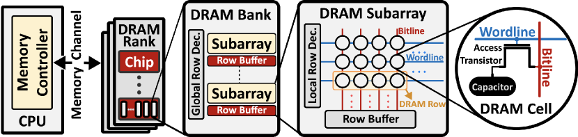
A typical computing system has one or more DRAM channels, where each channel has an independently operating I/O bus. As Fig. 1 illustrates, a Memory Controller (MC) interfaces with one or multiple DRAM ranks via the channel’s I/O bus. A DRAM rank consists of a group of DRAM chips that operate in lockstep. Because the I/O bus is shared across ranks, accesses to different ranks happen in serial manner. A DRAM chip is divided into multiple DRAM banks, each of which is further divided into multiple two dimensional DRAM cell arrays, called subarrays. Within each subarray, DRAM cells are organized as rows and columns. A DRAM cell connects to a sense amplifier via a bitline, and all sense amplifiers in the subarray form a row buffer. Within each DRAM cell, the data is stored as electrical charge on the capacitor and accessed through an access transistor. To perform a DRAM access, a row first must be activated (i.e., opened), which loads row’s data into the row buffer. A row activation is performed by enabling the wordline that corresponds to the row address that the MC provides along with the ACT command. To enable the corresponding wordline, the global row decoder first partially decodes the row address, and the local row decoder selects a wordline based on the partially decoded address provided by the global row decoder.
2.2 Accessing DRAM
To access a DRAM cell, the MC first needs to activate (i.e., open) the row that contains the cell by issuing an ACT command to a DRAM bank. A DRAM chip performs row activation in two steps. First, the wordline that corresponds to the row address is enabled to connect each cell capacitor in the row to its corresponding bitline. This causes charge sharing between a cell capacitor and a bitline. Due to the charge sharing, the bitline voltage slightly deviates from its pre-activation voltage level. Second, a sense amplifier detects the bitline voltage deviation and gradually restores the cell capacitor back to its original charge level. The data in the row buffer becomes accessible by a RD/WR command when the bitline and cell voltage is restored to a certain level. Therefore, the MC should follow an ACT with one or multiple RD/WR commands at least after the activation latency, which is typically denoted as tRCD.
To open a row in a bank that already has another row open, the MC first precharges the bank (i.e., closes the open row) by issuing a PRE command. The MC follows an ACT with a PRE at least after the restoration latency, which is typically denoted as tRAS. A DRAM chip performs a precharge operation in two steps. First, the DRAM chip disables the wordline of the activated row to disconnect its cells from the bitlines, and thus the row buffer. Second, the precharge circuitry, which is part of a sense amplifier, precharges the bitline to prepare it for the next row activation. The MC follows a PRE with an ACT to activate a new row at least after the precharge latency, which is typically denoted as tRP.
2.3 Periodic DRAM Refresh
A DRAM cell capacitor loses its charge over time [85, 86, 130], and losing too much charge results in a bit flip. The retention time of a cell refers to the duration for which its capacitor stores the correct value. Cells in a DRAM chip have different retention times, ranging from milliseconds to several hours [42, 56, 57, 65, 76, 84, 85, 86, 121, 124, 150]. However, to ensure data integrity, all DRAM cells are uniformly refreshed at fixed time intervals (typically 64, 32, or even ), called refresh window (tREFW). To perform periodic DRAM refresh, the MC issues a REF command at a fixed interval, denoted as refresh interval (tREFI) (typically 7.8 or ). A DRAM chip refreshes several (e.g., ) rows upon receiving a single REF command, and typically REF commands refresh the entire DRAM chip in a refresh window.
3 Motivation
In current DRAM chips, the Memory Controller (MC) is in charge of managing DRAM maintenance operations such as periodic refresh, RowHammer protection, and memory scrubbing. When DRAM vendors make modifications in a DRAM maintenance mechanism, the changes often need to be reflected to the MC design as well as the DRAM interface, which makes such modifications very difficult. As a result, implementing new or modifying existing maintenance operations requires multi-year effort by multiple parties that are part of the JEDEC committee. A prime example to support our argument is the most recent DDR5 standard [53], which took almost a decade to develop after the initial release of DDR4. DDR5 introduces changes to key issues we study in this paper: DRAM refresh, RowHammer protection, and memory scrubbing. We discuss these changes as motivating examples to show the shortcomings of the status quo in DRAM.
3.1 DRAM Refresh
DDR5 introduces Same Bank Refresh (SBR), which refreshes one bank in each bank group at a time instead of simultaneously refreshing all banks as in DDR4 [50, 96]. SBR improves bank availability as the MC can access the non-refreshing banks while certain banks are being refreshed. DDR5 implements SBR by introducing a new REFsb command [53]. This new command necessitates changes in the DRAM interface and in the MC design.
3.2 RowHammer Protection
In DDR4, DRAM vendors implement in-DRAM RowHammer protection mechanisms by performing Targeted Row Refresh (TRR) operations within the slack time available when performing regular refresh. However, prior works have shown that in-DRAM TRR is vulnerable to certain memory access patterns [41, 31, 48]. DDR5 specifies a Refresh Management (RFM) mechanism that an MC implements to aid the RowHammer protection implemented in DRAM chips. As part of RFM, the MC uses a set of counters to keep track of row activations to each DRAM bank. When a counter reaches a specified threshold value, the MC issues the new RFM command to DRAM chips. A DRAM chip then internally performs an undocumented operation with the time allowed for RFM to mitigate the RowHammer effect. Since the first RowHammer work [70] in 2014, it took about 7 years to introduce DDR5 RFM, which requires significant changes in the DRAM interface and the MC design. Still, RFM is likely not a definitive solution for RowHammer as it does not outline a specific RowHammer defense with security proof. Rather, RFM provides additional time to a DRAM chip for internally mitigating the RowHammer effect.
3.3 Memory Scrubbing
DDR5 adds support for on-die ECC and in-DRAM scrubbing. A DDR5 chip internally performs ECC encoding and decoding when the chip is accessed. To perform DRAM scrubbing, the MC must periodically issue the new scrub command (for manual scrubbing) or all-bank refresh command (for automatic scrubbing). Similar to Same Bank Refresh and RFM, enabling in-DRAM scrubbing necessitated changes in the DRAM interface and in the MC design.
4 Self-Managing DRAM
We introduce the Self-Managing DRAM (SMD) architecture.
4.1 Overview of SMD
SMD has a flexible interface that enables efficient implementation of multiple DRAM maintenance operations within the DRAM chip. Our key insight is to prevent the MC from accessing a DRAM row that is under maintenance by prohibiting the MC from activating the row until the maintenance is complete. The key idea of SMD is to provide a DRAM chip with the ability to reject an ACT command via a single-bit negative-acknowledgment (ACT_NACK) signal. An ACT_NACK informs the MC that the DRAM row it tried to activate is under maintenance, and thus temporarily unavailable. Leveraging the ability to reject an ACT, a maintenance operation can be implemented completely within a DRAM chip.
As Fig. 2 shows, SMD preserves the general DRAM interface222We consider the widely-available DDR4 as a baseline DRAM and explain the changes required to implement SMD on top of DDR4. However, other DRAM interfaces (e.g., DDR5, LPDDR5, GDDR6, HBM2) can also be modified in a similar way to support SMD. and only adds a single uni-directional pin to the physical interface of a DRAM chip. The extra pin is used for transmitting the ACT_NACK signal from the DRAM chip to the MC. Upon receiving an ACT_NACK, the MC notices that the previous row activation is rejected, and thus it need to be re-issued at later time. While introducing changes in the MC to handle ACT_NACK, SMD also simplifies MC design and operation as the MC no longer implements control logic to periodically issue DRAM maintenance commands. For example, the MC does not 1) prepare a bank for refresh by precharging it, 2) implement timing parameters relevant to refresh, nor 3) issue REF commands. The MC still maintains the bank state information (e.g., whether and which row is open in a bank) and respects the DRAM timing parameters associated with commands for performing access (e.g., ACT, PRE, RD, WR).
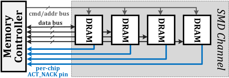
Fig. 3 shows the organization of a bank in an SMD chip. SMD divides the rows in a DRAM bank into multiple lock regions. SMD provides the number and the size of the lock regions to the MC via DRAM mode registers [50]. For each lock region, SMD stores an entry in a Lock Region Table (LRT) to indicate whether or not a lock region is reserved for performing a maintenance operation.
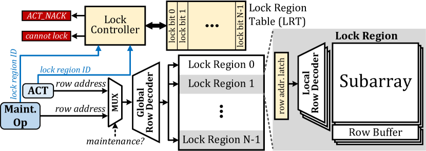
A maintenance operation and an ACT can be performed concurrently in the same bank on different lock regions. To enable this, SMD implements a row address latch in order to drive two local row decoders with two independent row addresses.333Having a row address latch per lock region enables two or more maintenance operations to concurrently happen on different lock regions within a bank. However, to keep our design simple, we restrict a maintenance operation to happen on one lock region while the MC can access another lock region. Our design can be easily extended to increase concurrency of maintenance operations across multiple lock regions. When a maintenance operation and an ACT arrive at the same lock region at the same time, the multiplexer shown in Fig. 3 prioritizes the maintenance operation and the SMD chip rejects the ACT.
For a maintenance operation to take place, the Lock Controller first sets the lock bit in the LRT entry that corresponds to the lock region on which the maintenance operation is to be performed. When the MC attempts to open a row in a locked region, the Lock Controller generates an ACT_NACK.
4.2 Handling an ACT_NACK Signal
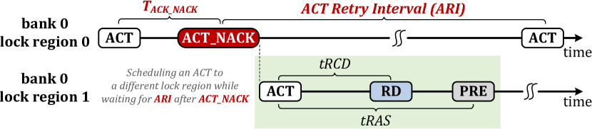
Fig. 4 depicts a timeline that shows how the MC handles an ACT_NACK signal. Upon receiving an ACT_NACK, the MC waits for ACT Retry Interval (ARI) time to re-issue the same ACT. It keeps re-issuing the ACT command once every ARI until the DRAM chip accepts the ACT. While waiting for ARI, the MC can attempt activating a row from a different lock region or bank, to overlap the ARI latency with a useful operation.
4.2.1 Setting the ACT Retry Interval (ARI)
Setting ARI to a very low or high value relative to the expected duration of the maintenance operations can have a negative impact on system performance and energy efficiency. When too low, the MC frequently re-issues an ACT, and the DRAM chip rejects many of these ACT commands. The rejected ACT commands waste energy and potentially delay other row activations that the MC could have issued to serve other memory requests. When ARI is too high, the MC may delay re-issuing a rejected ACT for too long, and the ACT gets delayed significantly even after the completion of the maintenance. We empirically find that is a favorable configuration for the five maintenance mechanisms that we evaluate in this work (section 5).
4.2.2 Latency
An SMD chip sends an ACT_NACK (in case an ACT command is to be rejected) DRAM command bus cycles after receiving the ACT. Thus, the MC knows that an ACT is successful when it does not receive an ACT_NACK in cycles after issuing the ACT. It is desirable for to be as low as possible so that the MC can be quickly notified when an ACT fails, and it can attempt to activate a different row in the same bank while waiting for ARI to retry the rejected ACT. Further, if is larger than tRCD, the latency of RD and WR commands increases (by ) as the MC should not issue a RD or WR without ensuring that the row is successfully opened.
The latency has three components: 1) the propagation delay (from the MC to the DRAM chip) of the ACT, 2) the latency of determining whether or not the row to be activated belongs to a locked region, and 3) the propagation delay (from the DRAM chip to the MC) of the signal.
We estimate the overall latency based on the latency of an RD in a conventional DRAM. An RD has a latency breakdown that resembles the latency breakdown of a . An RD command 1) propagates from the MC to the DRAM chip, 2) accesses data in a portion of the row buffer in the corresponding bank, and 3) sends the data back to the MC. In the DDR4 standard [50], the latency between issuing an RD and the first data beat appearing on the data bus is defined as tCL (typically 22 cycles for DDR4-3200). The latency components 1) and 3) of RD are similar to those of . Thus, the main difference between and tCL arises from the second component. According to our evaluation, the latency of accessing the Lock Region Table (LRT) is (section 7.6). Given the relatively low complexity of the LRT compared to the datapath that is involved during an RD, we believe the second component of the latency breakdown and thus the overall latency can be designed to be much smaller than tCL. We assume cycles unless stated otherwise. In our evaluations, we find that small latencies (e.g., ) have negligible effect on system performance mainly because the number of rejected ACTs constitute a small portion of all ACTs.
4.2.3 ACT_NACK Divergence Across DRAM Chips
SMD maintenance operations take place independently in each DRAM chip. Therefore, when a DRAM rank, which can be composed of multiple DRAM chips operating in lock step444DDRx systems typically consist of DRAM ranks built with multiple chips (e.g., eight chips with 8-bit data bus in each chip), whereas LPDDRx systems typically consist of DRAM ranks built with a single DRAM chip., receives an ACT command, some of the chips may send an ACT_NACK while others do not. As a result of this divergence, the row becomes partially open in chips that do not send ACT_NACK.
As a solution, the MC can take one of the following two approaches. First, it can issue a PRE command to close the partially open row. Upon receiving the PRE, chips that sent an ACT_NACK and do not have an open row can simply ignore the PRE. The advantage of this approach is that, after the PRE, the MC can attempt to open another row from the same bank. However, as a downside, precharging the partially activated row would waste energy. As a second approach, the MC can wait for ARI and re-issue the same ACT command to attempt activating the row in the chips that previously sent an ACT_NACK signal. This approach does not waste row activation energy but it prevents the MC from attempting to activate another row in the same bank while waiting for ARI. We empirically find that the second approach performs slightly better (by 0.04% on average) mainly because the benefits of the first approach are limited as a partially activated row cannot be immediately precharged due to tRAS, which constitutes a large part of ARI555By default, we set while tRAS is about [96].).
Ensuring forward progress for memory requests. SMD does not cause deadlocks, livelocks or other starvation issues because of the following three characteristics. We use a memory controller design that periodically reissues the ACT command to an ACT_NACK’d region until the command does not get ACT_NACK’d to serve the highest priority memory request. If a high-priority request is ACT_NACK’d, it is in the memory request scheduling algorithm’s best interest to keep issuing ACT commands to the locked region until the lock is released (as opposed to scheduling another request with a lower priority to a potentially not-locked region). Based on this memory controller design, we explain how SMD prevents resource starvation issues. First, a DRAM chip remains idle for ARI between the end of a maintenance operation and the start of the next maintenance operation (Section 4.2). Second, the MC periodically re-issues an ACT every ARI to serve the memory request with the highest priority. Third, a DRAM chip cannot start performing a maintenance operation when one of its rows is active. If a DRAM chip issues an ACT_NACK command, the periodically issued (every ARI) ACT commands will activate the row in this chip after the maintenance operation ends. Meanwhile, other DRAM chips that did not issue an ACT_NACK command cannot start issuing ACT_NACK commands because these chips already have the DRAM row activated. Thus, the maximum memory request stall time is the time it takes a DRAM chip to perform the most time taking maintenance operation. To limit the maximum potential memory request stall time, 1) long time taking maintenance operations can be divided into many smaller short time taking maintenance operations, 2) the maximum time a maintenance operation takes can be specified in the DRAM standard. In our design, the most time taking maintenance operation is SMD-FR (Section 5.1.1), which takes to refresh 16 DRAM rows in a lock region.
4.3 Region Locking Mechanism
SMD locks rows at a lock region granularity.
4.3.1 Locking a Region
A maintenance operation can be performed on a lock region only after locking it. Therefore, a maintenance mechanism must lock the region that includes the rows that should undergo a maintenance. A maintenance mechanism can only lock a region that is not already locked. This is to prevent different maintenance mechanisms from interfering with each other. Two maintenance operations can concurrently proceed if they target different lock regions.666An ECC scrubbing operation (Section 5.3) uses the data bus, which is a shared resource across all regions. Therefore, a scrubbing operation locks all regions at once to prevent any other maintenance operation or memory access from happening at the same time. Once having locked a region, the region remains locked until the completion of the maintenance. Afterward, the maintenance mechanism releases the lock to allow 1) the MC to access the region and 2) other maintenance mechanisms to lock the same region.
4.3.2 Lock Region Size
A lock region consists of a fixed number of consecutively-addressed DRAM rows. To simplify the design, we set the lock region size such that a lock region spans one or multiple subarrays. This is because a maintenance operation uses the local row buffers in a subarray, and thus having a subarray shared by multiple lock regions will cause a conflict when accessing a row in a different lock region that maps to the subarray under maintenance. We design and evaluate SMD assuming a default lock region size of 512-row subarrays. However, a lock region can be designed to span fewer than subarrays or it can span the entire bank.
Modern DRAM chips typically use the density-optimized open-bitline architecture [1, 47], which places sense amplifiers both on top and bottom sides of a subarray and adjacent subarrays share sense amplifiers. With the open-bitline architecture, the MC should not be allowed to access a row in a subarray that is adjacent to one under maintenance. To achieve this, the Lock Controller simply sends an ACT_NACK when the MC attempts to activate a row in a subarray adjacent to a subarray in a locked region. Consequently, when SMD locks a region that spans 512-row subarrays, it prevents the MC from accessing subarrays in a bank with rows ( subarrays). In the folded-bitline architecture [1, 47], adjacent subarrays do not share sense amplifiers with each other. Therefore, SMD prevents access only to the subarrays in a locked region. We evaluate SMD using the density-optimized open-bitline architecture.
4.3.3 Ensuring Timely Maintenance Operations
A maintenance mechanism cannot lock a region that has an active DRAM row. To lock the region, the maintenance mechanism must wait for the MC to precharge the row. The MC may keep a DRAM row active for too long, which may delay a maintenance operation to a point that affects DRAM reliability (e.g., delaying a refresh operation too long as such a retention failure occurs). To prevent this, we rely on the existing time limit for a row to remain open, i.e., tRAS has an upper limit of 9x tREFI [50, 96, 45]).
Predictability and Performance Guarantees. The key drawback of our SMD implementation is that it makes the synchronous DDRx interface less predictable. However, the practical performance overheads of this drawback are very low, as we demonstrate in Section 7. In a system without SMD, an already determined optimal DRAM command schedule executes as intended (without random delays) as the DDRx interface is synchronous. However, in an SMD system, an optimal schedule could have to be periodically recreated to remain optimal because the DRAM chips can reject activations and induce non-deterministic latency for memory requests. In this paper, we comprehensively describe only one out of many different possible implementations of SMD due to page limits. This implementation prioritizes simplicity. However, the DRAM standard can more strictly specify exactly when and for how long SMD chips are allowed to perform maintenance operations. This stricter implementation would make SMD chips as predictable as DDRx chips today. We hope that future work building on SMD will comprehensively address these issues. To make it more evident that SMD can be implemented in a way that preserves the predictability of the DDRx interface from the perspective of the memory controller (i.e., in a way that keeps the DRAM interface synchronous), we describe a (more) predictable SMD standardization.
Designing a Predictable SMD Interface. A simple way of preserving the DDRx interface’s synchronicity with SMD is to allow the DRAM chip to perform a maintenance operation periodically only at well-defined time intervals. In other words, the DRAM chip can respond with ACT_NACKs only for the fraction of time during which the chip is allowed to execute maintenance operations. We call this fraction of time the maintenance operation time (MOT). Outside of MOT, the DDRx operates as defined today (i.e., synchronously and predictably). During an MOT, the memory controller is allowed to access DRAM cells at the cost of potentially getting ACT_NACK’d by the DRAM chip. The new SMD standard would specify i) how long an MOT is, ii) the period at which the interface enters an MOT, iii) how entry to an MOT is triggered (e.g., by a new MOT command), and iv) how many MOTs the memory controller can postpone.
5 SMD Maintenance Mechanisms
We propose SMD-based maintenance mechanisms for three use cases. However, SMD is not limited to these three use cases and it can be used to support more operations in DRAM.
5.1 Use Case 1: DRAM Refresh
In conventional DRAM, the MC periodically issues REF commands to initiate a DRAM refresh operation. This approach is inefficient due to three main reasons. First, transmitting REF commands over the DRAM command bus within the refresh period (e.g., 64, 32, or even depending on the refresh rate) consumes energy and increases the command bus utilization. Due to transmitting a REF over the command bus, the MC may delay a command to another rank in the same channel, which increases DRAM access latency [16]. Second, an entire bank becomes inaccessible while being refreshed although a REF command refreshes only a few rows in the bank. This incurs up to 50% loss in memory throughput [86]. Third, new mechanisms that reduce refresh overhead (e.g., by skipping refreshes on retention-strong rows) are difficult to implement. Even a simple optimization of enabling per-bank refresh in DDR4 requires changes to the DRAM interface and the MC.
Leveraging SMD, we design two maintenance mechanisms for DRAM refresh: Fixed-Rate Refresh and Variable Refresh.
5.1.1 Fixed-Rate Refresh (SMD-FR)
SMD-FR refreshes DRAM rows in a fixed time interval (i.e., tREFI), similar to conventional DRAM refresh. It enables refresh-access parallelization without any burden on the MC beyond the changes required for implementing the SMD interface. As with any maintenance operation in SMD, the MC can activate a row (in any bank) in regions that are not locked while SMD-FR refreshes rows in a locked region. SMD-FR refreshes (Refresh Granularity) number of rows from a lock region and switches to refreshing another region to 1) limit the time for which a single lock region remains under maintenance and 2) prevent memory requests from waiting too long for the region to become available for access.
SMD-FR operates independently in each DRAM bank and SMD-FR uses three counters for managing the refresh operations in a bank: pending refresh counter, lock region counter, and row address counter. Fig. 5 illustrates SMD-FR operation. The pending refresh counter is used to slightly delay refresh operations within the slack777DDR4 [50, 96, 45] allows the MC to postpone issuing up to REF commands in order to serve pending memory requests first. given in the DRAM standard until the region to be refreshed can be locked. The pending refresh counter is initially zero and SMD-FR increments it by one at the end of a tREFI interval . SMD-FR allows up to refresh operations to be accumulated in the pending refresh counter. As we explain in section 4.3.3, because the MC can keep a row open for a limited time, the pending refresh counter never exceeds the value , and this is how SMD ensures that the refresh operations do not lag behind more than the window of refresh operations.
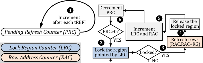
The lock region and row address counters indicate the next row to refresh. When pending refresh counter is greater than zero, SMD-FR attempts to lock the region indicated by the lock region counter every clock cycle until it successfully locks the region . In some cycles, SMD-FR may fail to lock the region either because the lock region contains an active row or the region is locked by another maintenance mechanism. When SMD-FR successfully locks the region, it initiates a refresh operation that refreshes number of sequentially-addressed rows in the lock region starting from the row indicated by the row address counter . The refresh operation is carried out similarly as in conventional DRAM, essentially by activating and precharging a row to restore the charge in its DRAM cells. Making larger increases the latency of a single refresh operation, which prolongs the time that a lock region remains unavailable for access. In contrast, small causes switching from one lock region to another very often, increasing interference with accesses. We empirically find to be a favorable design point.
After the refresh operation completes, SMD-FR releases the locked region and increments only the lock region counter. When the lock region counter rolls back to zero, SMD-FR also increments by one the row address counter . Finally, SMD-FR decrements the target refresh counter .
5.1.2 Variable Refresh (SMD-VR)
In conventional DRAM, all DRAM rows are uniformly refreshed with the same refresh period. However, the actual data retention times of different rows in the same DRAM chip greatly vary mainly due to manufacturing process variation and design-induced variation [86, 124, 85, 121, 78, 107]. In fact, only hundreds of “weak” rows across an entire DRAM chip require to be refreshed at the default refresh rate, and a vast majority of the rows can correctly operate when the refresh period is doubled or quadrupled [86]. Eliminating unnecessary refreshes to DRAM rows that do not contain weak cells can significantly mitigate the performance and energy consumption overhead of DRAM refresh [86].
We develop Variable Refresh (SMD-VR), a mechanism that refreshes different rows at different refresh rates depending on the retention time characteristics of the weakest cell in each row. SMD enables implementing SMD-VR with no further changes in the DRAM interface and the MC. Our SMD-VR design demonstrates the versatility of SMD in supporting different DRAM refresh mechanisms.
The high-level idea of SMD-VR is to group DRAM rows into multiple retention time bins and refresh a DRAM row based on the retention time bin that it belongs to. To achieve low design complexity, SMD-VR uses only two bins: 1) retention-weak rows that have retention time less than and 2) rows that have retention time more than . Inspired by RAIDR [86], SMD-VR stores the addresses of retention-weak rows using a per-bank Bloom Filter [10], which is a space-efficient probabilistic data structure for representing set membership. We assume retention-weak rows are already inserted into the Bloom Filters by the DRAM vendors during post-manufacturing tests.888Alternatively, SMD can be used to develop a maintenance mechanism that performs retention profiling. We believe SMD enables such profiling in a seamless way. Due to limited space, we leave the development and analysis of it to future work.
The operation of SMD-VR resembles the operation of SMD-FR with the key difference that SMD-VR sometimes skips refreshes to a row that is not in the Bloom Filter, i.e., a row with high retention time. Fig. 6 illustrates how SMD-VR operates. SMD-VR uses the same three counters as SMD-FR. SMD-VR also uses a refresh cycle counter, which is used to indicate the refresh period when all rows (including retention-strong rows) must be refreshed. The refresh cycle counter is initially zero and gets incremented at the end of every refresh period, i.e., when the entire DRAM is refreshed.
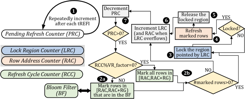
SMD-VR increments the pending refresh counter by one at the end of a tREFI interval . When the pending refresh counter is greater than zero, SMD-VR determines whether or not the number of rows, starting from the address indicated by the lock region and row address counters, are retention-weak rows by testing their row addresses using the bank’s Bloom Filter . SMD-VR refreshes the rows that are present in the Bloom Filter every time when it is their turn to be refreshed, as indicated by the lock region and row address counters. In contrast, SMD-VR refreshes the rows that are not present in the Bloom Filter only when the refresh cycle counter has a value that is multiple of , which is specified by Equation 1.
| (1) |
Unless stated otherwise, we assume and . Therefore, SMD-VR refreshes the DRAM rows that are not in the Bloom Filter once every four consecutive refresh periods as these rows can retain their data correctly for at least four refresh periods.
After determining which DRAM rows need refresh, SMD-VR operates in a way similar to SMD-FR.
5.2 Use Case 2: RowHammer Protection
RowHammer is a DRAM reliability issue mainly caused due to the small DRAM cell size and the short cell-to-cell distance in modern DRAM chips. Repeatedly activating and precharging (i.e., hammering) a (aggressor) DRAM row creates a disturbance effect, which accelerates charge leakage and causes bit errors in the cells of a nearby (victim) DRAM row [158, 33, 54, 113, 114, 127, 151, 157].
The three major DRAM manufacturers equip their existing DRAM chips with in-DRAM RowHammer protection mechanisms, generally referred to as Target Row Refresh (TRR) [41, 31, 48]. At a high level, TRR protects against RowHammer by detecting an aggressor row and refreshing its victim rows. Because a conventional DRAM chip cannot initiate a refresh operation by itself, TRR refreshes victim rows by taking advantage of the slack time available in the refresh latency (i.e., tRFC), originally used to perform only periodic DRAM refresh [41, 31, 48]. This approach has two major shortcomings that limit the protection capability of TRR [41]. First, the limited slack time in tRFC puts a hard constraint on the number of TRR-induced refreshes. This restriction results in insufficient protection to victim rows, especially when DRAM becomes more RowHammer vulnerable with DRAM technology scaling. Second, TRR-induced refresh takes place only at a certain rate (i.e., at most on every REF ). Recent works [41, 31, 48, 24] demonstrate a variety of new RowHammer access patterns that circumvent the TRR protection in chips of all three major DRAM vendors, proving that the existing DRAM interface is not well suited to enable strong RowHammer protection especially as RowHammer becomes a bigger problem with DRAM technology scaling.
We use SMD to develop two maintenance mechanisms that overcome the limitations of the existing TRR mechanisms by initiating victim row refresh within the DRAM chip.
5.2.1 Probabilistic RowHammer Protection
Inspired by PARA [70], we implement an in-DRAM maintenance mechanism called Probabilistic RowHammer Protection (SMD-PRP). The high level idea is to refresh the nearby rows of an activated row with a small probability. PARA is proposed as a mechanisms in the MC, which makes it difficult to adopt since victim rows are not always known to the MC. SMD enables us to overcome this issue by implementing the PARA-inspired SMD-PRP mechanism completely within the DRAM chip. In addition, SMD-PRP avoids explicit ACT and PRE commands to be sent over the DRAM bus. Fig. 7 illustrates the operation of SMD-PRP.
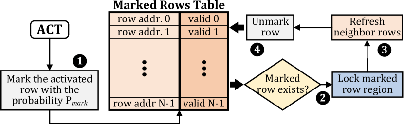
On a DRAM row activation, SMD-PRP marks the activated row as an aggressor with a small probability of . It marks an aggressor row using a per-bank Marked Rows Table (MRT), that contains an entry for each lock region in the bank. An entry consists of the marked row address and a valid bit. The bit length of the address depend on the size of a lock region. For example, an MRT entry has a 13-bit address field when the lock region size is rows. When MRT contains a marked row, SMD-PRP locks the corresponding region and refreshes the neighbor rows of the marked row . This step can easily accommodate blast radius [155] and any address scrambling. Once the neighbor rows are refreshed, SMD-PRP unlocks the region and unmarks the row in MRT .
5.2.2 SMD-PRP with Aggressor Row Detection
SMD-PRP refreshes victim rows with a small probability on every row activation, even does so for a row that has been activated only a few times. This results in unnecessary victim refreshes, especially for high values that strengthen the RowHammer protection as DRAM cells become more vulnerable to RowHammer with technology scaling.
We propose SMD-PRP+, which detects potential aggressor rows and probabilistically refreshes only their victim rows. The key idea of SMD-PRP+ is to track frequently-activated rows in a DRAM bank and refresh the neighbor rows of these rows using the region locking mechanism of SMD.
SMD-PRP+ tracks frequently-activated rows, within a rolling time window of length , using two Counting Bloom Filters (CBF) [29] that operate in time-interleaved manner. CBF is a Bloom Filter variant that represents the upperbound for the number of times an element is inserted into the CBF. We refer the reader to prior work for background on CBFs [155, 122].
Depicted in Fig. 8, SMD-PRP+ operation is based on 1) detecting a row that has been activated more than times within the most recent interval and 2) refreshing the neighbor rows of this row. must be set according to the minimum hammer count needed to cause a RowHammer bit flip in a given DRAM chip. A recent work shows that activations can cause bit flips in LPDDR4 chips [62]. We conservatively set to . must be equal to or larger than the refresh period in order to track all activations that happen until rows get refreshed by regular refresh operations. We set equal to the refresh period.
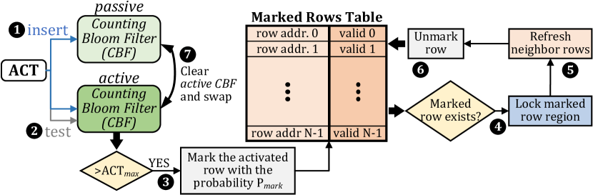
Initially, one of the CBFs is in active mode while the other is in passive mode. When activating a row, SMD-PRP+ inserts the address of the activated row to both CBFs . Then, SMD-PRP+ tests the active CBF to check if the accumulated insertion count exceeds the threshold . If so, SMD-PRP+ marks the row in the Marked Rows Table to refresh its neighbor rows with the probability of . SMD-PRP+ does not always mark the row because it is impossible to reset only the counters that correspond to the marked row address in the CBFs. If always marked, a subsequent activation of the same row would again cause the row to be marked, leading to unnecessary neighbor row refresh until all CBF counters are reset, which happens at the end of the interval. After a row is marked, steps - are same as steps - in SMD-PRP. Finally, at the end of an interval, SMD-PRP+ clears the active CBF and swaps the two CBFs to continuously track row activations within the most recent window .
5.2.3 Deterministic RowHammer Protection
SMD-PRP and SMD-PRP+ are probabilistic mechanisms that provide statistical security against RowHammer attacks with being the security parameter. On an extremely security-critical system, a deterministic RowHammer protection mechanisms can guarantees mitigation of RowHammer bit flips at all times.
We use SMD to implement SMD-DRP, a deterministic RowHammer protection mechanism based on the Graphene [116] mechanism, which uses the Misra-Gries algorithm [97] for detecting frequent elements in a data stream to keep track of frequently activated DRAM rows. Graphene is provably secure RowHammer protection mechanism with zero chance to miss an aggressor row activated more than a predetermined threshold. Different from Graphene, we implement SMD-DRP completely within a DRAM chip by taking advantage of SMD, whereas Graphene requires the memory controller to issue neighbor row refresh operations when necessary.
The key idea of SMD-DRP is to maintain a per-bank Counter Table (CT) to track the most-frequently activated DRAM rows within a certain time interval (e.g., refresh period of tREFW). Fig. 9 illustrates the operation of SMD-DRP.
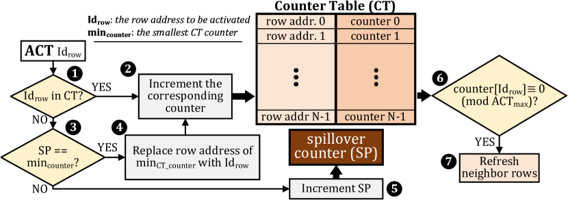
When SMD-DRP receives an ACT, it check if the activated row address () is already in CT . If so, SMD-DRP increments the corresponding counter in CT by one . If is not in CT, SMD-DRP finds the smallest counter value () in CT and compares it to the value of the spillover counter (SP) , which is initially zero. If SP is equal to , SMD-DRP replaces the row address corresponding to in CT with and increments the corresponding CT counter by one . If SP is smaller than , SMD-DRP increments SP by one . When a CT counter is incremented in step , SMD-DRP checks if the counter value is a multiple of , which is the maximum number of times a row can be activated without refreshing its neighbors. If so, SMD-DRP refreshes the neighbors of . To prevent the counters from overflowing, SMD-DRP resets the CT counters and SP on every tREFW interval.
To ensure that no row is activated more than without refreshing its neighbor rows, the number of CT counters () must be configured according to the following formula:
| (2) |
where is the maximum number of activations that the memory controller can perform within a tREFW interval in a single bank.
We refer the reader to [116] for more details on the Graphene mechanism and its security proof. The operation of SMD-DRP is similar to the operation of Graphene with the difference of SMD-DRP being implemented completely within a DRAM chip, which does not affect the underlying operation, and thus the security proof of Graphene applies to SMD-DRP.
5.3 Use Case 3: Memory Scrubbing
To mitigate the increasing bit error rates that are mainly caused by the continued DRAM technology scaling, DRAM vendors equip their DRAM chips with on-die Error Correction Codes (ECC) [120, 119, 109, 56]. On-die ECC is designed to correct a single bit error assuming that a failure mechanism is unlikely to incur more than one bit error in a codeword [119]. However, even when the assumption always holds, a failure mechanism can gradually incur two or more bit errors over time. A widely-used technique for preventing the accumulation of an uncorrectable number of bit errors is memory scrubbing. Memory scrubbing describes the process of periodically scanning the memory for bit errors in order to correct them before more errors occur.
We propose SMD-based Memory Scrubbing (SMD-MS), which is an in-DRAM maintenance mechanism that periodically performs scrubbing on DRAM chips with on-die ECC. Using SMD, we implement SMD-MS without any further changes to the DRAM interface and the MC. Compared to conventional MC-based scrubbing, SMD-MS eliminates moving data to the MC by scrubbing within the DRAM chip, and thus reduces the performance and energy overheads of memory scrubbing.
SMD-MS operation resembles the operation of SMD-FR. Similar to SMD-FR, SMD-MS maintains pending scrub counter, lock region counter, and row address counter. SMD-MS increments the pending scrub counter at fixed intervals of . When the pending scrub counter is greater than zero, SMD-MS attempts to lock the region indicated by the lock region counter. After locking the region, SMD-MS performs scrubbing operation on the row indicated by the row address counter. The scrubbing operation takes more time than a refresh operation as performing scrubbing on a row consists of three time consuming steps for each codeword in the row: 1) reading the codeword, 2) performing ECC decoding and checking for bit errors, and 3) encoding and writing back the new codeword into the row only when the decoded codeword contains a bit error. Refreshing a row takes , whereas scrubbing a row takes when no bit errors are detected.999We assume ECC decoding/encoding hardware is fully pipelined. In case of a bit error, writing a corrected codeword incurs additional latency. Therefore, SMD-MS keeps a region locked for much longer than SMD-FR. When the scrubbing operation is complete, SMD-MS releases the lock region and increments the lock region and row address counters, and decrements the pending scrub counter as in SMD-FR.
6 Experimental Methodology
We extend Ramulator [72, 128] to implement and evaluate the five SMD maintenance mechanisms (SMD-FR, SMD-VR, SMD-PRP, SMD-PRP+, and SMD-MS) that we describe in section 5. We use DRAMPower [2, 14] to evaluate DRAM energy consumption. We use Ramulator in CPU-trace driven mode executing traces of representative sections of our workloads collected with a custom Pintool [88]. We warm-up the caches by fast-forwarding 100 million instructions. We simulate each representative trace for 500 million instructions (for multi-core simulations, we simulate until each core executes at least 500 million instructions). We release the source code of modified version of Ramulator openly and freely available at [133].
We use the system configuration provided in Table 1 in our evaluations. Although our evaluation is based on DDR4 DRAM, the modifications required to enable SMD can be adopted in other DRAM standards, as we explain in section 7.6.
| Processor | & 4-wide issue CPU core, 1-4 cores, 8 MSHRs/core, 128-entry instruction window |
| Last-Level Cache | cache-line, 8-way associative, /core |
| Memory Controller | 64-entry read/write request queue, FR-FCFS-Cap [104] |
| DRAM | DDR4-3200 [50], refresh period, 4 channels, 2 ranks, 4/4 bank groups/banks, 128K-row bank, 512-row subarray, row size |
Workloads. We evaluate 44 single-core applications from four benchmark suites: SPEC CPU2006 [144], TPC [147], STREAM [93], and MediaBench [32]. We classify the workloads in three groups based on their memory intensity, which we measure using misses-per-kilo-instructions (MPKI) in the last-level cache (LLC). The low, medium, and high memory intensity groups consist of workloads with , , and . We randomly combine single-core workloads to create multi-programmed workloads. Each multi-programmed workload group, 4c-low, 4c-medium, and 4c-high, contains four-core workloads with low, medium, and high memory intensity.
7 Evaluation
We evaluate the performance and energy efficiency of SMD-based maintenance mechanisms.
7.1 Single-core Performance
Fig. 10 shows the speedup of single-core workloads when using the following maintenance mechanisms: 1) SMD-FR, 2) SMD-VR, 3) SMD-PRP, 4) SMD-PRP+, 5) SMD-MS, and 6) the combination of SMD-VR, SMD-PRP, and SMD-MS (SMD-Combined).101010We individually evaluate SMD-PRP, SMD-PRP+, and SMD-MS using SMD-FR as a refresh mechanism since SMD-FR is very simple and easy to implement. In SMD-Combined, we prefer SMD-PRP over SMD-PRP+ to keep the DRAM chip area overhead minimal. Based on [86], for SMD-VR, we conservatively assume 0.1% of rows in each bank need to be refreshed every while the rest retain their data correctly for and more. SMD-VR uses a -bit Bloom Filter with hash functions. SMD-PRP and SMD-PRP+ refresh the victims of an activated row with a high probability, i.e., . SMD-MS operates with an aggressive 5-minute scrubbing period. 111111We analyze SMD-PRP, SMD-PRP+, and SMD-MS at various configurations and find that their overheads are relatively low even at more aggressive settings. We omit the details due to space limitations. We calculate the speedup compared to DDR4 DRAM with a nominal refresh period. To demonstrate the maximum speedup achievable by eliminating the entire DRAM refresh overhead, Fig. 10 also includes the performance of hypothetical DRAM that does not require refresh (NoRefresh). The figure shows workloads that have at least 10 Last-Level Cache Misses per Kilo Instruction (MPKI). GMEAN-22 provides the geometric mean of the workloads and GMEAN-ALL of all single-core workloads that we evaluate.
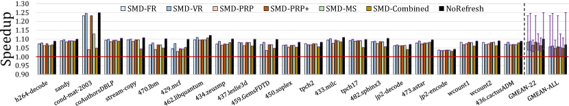
We make five key observations. First, SMD-FR provides 5.7% average speedup (up to 23.2%) over conventional DDR4 refresh (84.1% of the speedup that NoRefresh provides). Although SMD-FR and DDR4 have similar average latency to refresh a single DRAM row, SMD-FR outperforms DDR4 refresh due to two main reasons: 1) enabling concurrent access and refresh of two different lock regions within a DRAM bank and 2) completely eliminating the REF commands on the DRAM commands bus to reduce the command bus utilization. SMD-FR requires very low area overhead and no information with respect to DRAM cell characteristics, yet provides significant speedup.
Second, SMD-VR provides 6.1% average speedup (up to 24.5%), achieving 89.9% of the speedup that NoRefresh provides. SMD-VR provides higher speedup due to eliminating unnecessary refresh operations to retention-strong rows. Compared to SMD-FR, SMD-VR’s performance benefits are limited because SMD-FR significantly mitigates the refresh overhead by overlapping refresh operations with accesses to other lock regions, leaving small opportunity for further improvement by skipping refreshes to retention-strong rows.
Third, both SMD-FR and SMD-VR perform close to the hypothetical “NoRefresh” DRAM. On average, SMD-FR/SMD-VR provide 83.8%/86.8% of the speedup that “NoRefresh” provides compared to the DDR4 baseline.
Fourth, although the overheads of the SMD-PRP, SMD-PRP+, and SMD-MS mechanisms partially negate the performance benefits of SMD-FR, they still achieve average (maximum) speedup of 4.7%/5.7%/5.4% (9.4%/23.2%/12.9) over the DDR4 baseline, when integrated on top of SMD-FR.
Fifth, SMD-Combined improves performance by 4.8% (up to 10.6%), showing that SMD enables robust RowHammer protection and frequent (5-minute) memory scrubbing while still improving system performance.
7.2 Multi-core Performance
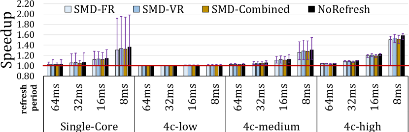
Fig. 11 shows weighted speedup (normalized to the weighted speedup of the DDR4 baseline) for 60 four-core workloads (20 per memory intensity level). The bars (error lines) represent the average (minimum and maximum) weighted speedup across the 20 workloads in the corresponding group. We make three major observations.
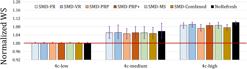
First, we observe the largest average speedup in memory-intensive four-core workloads, i.e., 4c-high. SMD-FR/SMD-VR improve average speedup by 8.7%/9.2% (9.9%/10.2 maximum), which corresponds to 86.8%/91.2% of the speedup that hypothetical “NoRefresh” achieves over DDR4.
Second, combining SMD-VR+SMD-PRP+SMD-MS provides 7.6% average (9.1% maximum) improvement in weighted speedup, which indicates that SMD-PRP and SMD-MS incur only small performance overhead on top of SMD-VR.
Third, the performance benefits become smaller as the memory intensity of the workloads decrease. Specifically, 4c-medium achieves lower speedup than 4c-high, and 4c-low achieves lower speedup than 4c-medium.
Performance Summary. The new DRAM refresh mechanisms SMD-FR and SMD-VR significantly improve system performance, achieving speedup close to that provided by the hypothetical “NoRefresh” DRAM. SMD enables efficient and robust RowHammer protection (SMD-PRP and SMD-PRP+) and memory scrubbing (SMD-MS) that still provide significant speedup when integrated with SMD-FR. Overall, SMD enables DRAM that is both faster and more robust than DDR4.
7.3 Energy Consumption
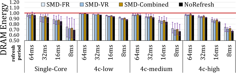
Fig. 12 shows the average DRAM energy consumption normalized to the DDR4 baseline for single- and four-core workloads. We make three major observations.
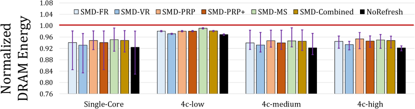
First, SMD-FR reduces DRAM energy for both single- and four-core workloads (by 5.9% and 5.5% on average) over DDR4 mainly due to reduction in execution time.
Second, SMD-VR reduces DRAM energy by 6.8%/6.7% on average for single-core and 4c-high workloads by especially eliminating some unnecessary refresh operations. The maximum DRAM energy reduction that can be achieved by completely eliminating DRAM refresh operation is 7.8% as indicated by “NoRefresh” DRAM.
Third, SMD-Combined reduce DRAM energy by 5.2% for both single-core and 4c-high workloads. This shows that the energy overhead of SMD-PRP and SMD-MS are small.
The new SMD-based refresh mechanisms eliminate most of the energy overhead of DRAM refresh. SMD-based RowHammer protection and memory scrubbing improve DRAM reliability and security with low DRAM energy cost.
7.4 Isolating SMD’s Performance Benefits
We evaluate SMD’s performance without the added benefits of memory accesses and maintenance operation parallelization (i.e., SMD with a single lock region) using all four-core heavily memory-intensive (4c-high) workloads. This configuration of SMD, called SMD-Combined-1LR, implements the same maintenance mechanisms as SMD-Combined does. We compare SMD-Combined-LR to SMD-Combined. We also evaluate a DRAM chip that leverages refresh-access parallelization [16, 161], called DSARP. A system that implements DSARP can parallelize refresh and memory access operations to different subarrays. We compare DSARP to SMD-FR. Figure 13 shows the speedup of 4-core workloads using these three mechanisms (SMD-FR, DSARP, SMD-Combined-1LR) and NoRefresh.
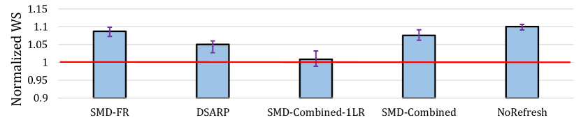
We make two major observations from Figure 13. First, SMD-Combined-1LR improves performance by 0.9% (3.2%) on average (at maximum) across all workloads. SMD-Combined-1LR improves performance less than (and sometimes degrades performance) SMD-Combined because it cannot concurrently perform maintenance operations and memory accesses. Second, DSARP improves performance by 5.0% (6.0%) on average (at maximum) across all workloads. We conclude that being able to concurrently execute maintenance and memory access operations at the same time increases SMD’s performance benefits, and SMD-FR provides comparable performance benefits to a DRAM chip that can leverage refresh-access parallelization (DSARP).
7.5 Sensitivity Studies
We analyze the performance and DRAM energy effects of different SMD configuration parameters.
7.5.1 DRAM Refresh Period
Fig. 14 plots the speedup and energy reduction that SMD-FR, SMD-VR, and SMD-combined achieve over DDR4 for different refresh periods across single- and four-core workloads. We make three key observations. First, the performance and energy benefits of SMD-FR/SMD-VR increase as the refresh period reduces, achieving 50.5%/53.6% speedup and 25.6%/29.0% DRAM energy reduction on average at refresh period across 4c-high workloads. Thus, SMD-based refresh mechanisms will become even more beneficial to employ in future DRAM chips that are expected to require more frequent refresh [86, 56, 85]. Second, SMD-combined provides 51.5% speedup and 27.9% DRAM energy reduction on average across 4c-high at refresh period, showing that the overheads of SMD-based RowHammer protection and memory scrubbing mechanisms remain low even at high refresh rates. Third, all SMD-based maintenance mechanism eliminate most of the performance overhead of refresh across all refresh periods (e.g., SMD-combined reaches 95.6% of the hypothetical NoRefresh DRAM at ).
We conclude that SMD-based maintenance mechanisms improve DRAM reliability and security while greatly reducing the overhead of DDR4 refresh. Their performance benefits are expected to increase for future DRAM chips that are likely to require high refresh rates.
7.5.2 Lock Region Size
The size of a SMD lock region affects the performance and energy of SMD-based maintenance mechanisms. Generally, it is desirable to have many small-sized lock regions to enable locking smaller portions of the DRAM chip for maintenance and allow accesses to non-locked regions. However, the DRAM chip area overhead of SMD increases as the number of lock regions in a bank increase. We analyze the performance and energy impact of different lock region size configurations.
We use the following equation to calculate the number of lock regions per bank () by dividing the number of rows in a bank () to the number of rows in a lock region ().
| (3) |
Figure 15 shows the speedup and DRAM energy savings that SMD-FR, SMD-VR, and SMD-Combined achieve for different number of lock regions per bank across 4c-high workloads. We make two key observations. First, with a single lock region per bank, SMD-FR/SMD-Combined on average perform 3.7%/8.9% worse than the DDR4 baseline, which leads to 3.2%/10.7% higher average DRAM energy consumption. This is because a maintenance operation locks the entire bank, and thus the MC waits for ARI upon receiving an ACT_NACK to issue another ACT to the same bank. Although SMD-VR suffers from the same issue, it still outperforms the baseline by eliminating unnecessary refreshes to rows with high retention times.
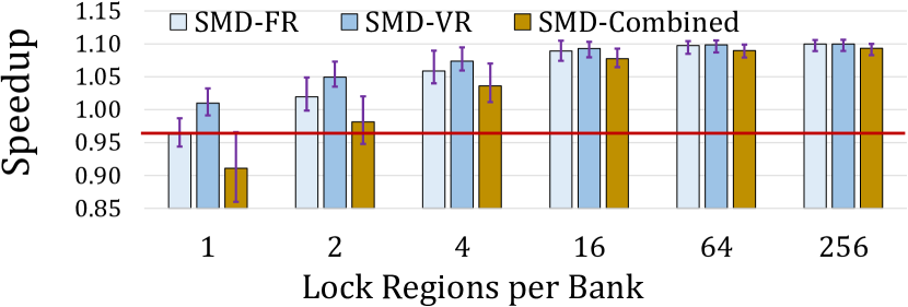
Second, when the lock regions are smaller, and thus a bank has four or more lock regions, all mechanisms outperform the baseline for all 4c-high workloads and save DRAM energy. This shows that even a small number of lock regions are sufficient to overlap the maintenance operation latency with accesses to non-locked regions.
Third, the performance and energy benefits of increasing the number of lock regions gradually diminish. We find that 8192-row lock regions incur low area overhead and achieve a significant portion of the speedup that smaller lock regions provide (e.g., SMD-Combined achieves 7.7%/9.3% speedup with 16/256 lock regions). Therefore, by default, we use lock regions per bank in our evaluations.
We conclude that SMD significantly reduces the overhead of DRAM maintenance operations even with large lock regions.
7.5.3 ACT_NACK Divergence Across Chips
In Section 4.2, we explain divergence in SMD maintenance operations can happen when different DRAM chips in the same rank perform maintenance operation at different times. Such a divergence leads to a partial row activation when the activated row is in a locked region in some DRAM chips but not in others. To handle partial row activations, we develop three policies.
Precharge. With the Precharge policy, the MC issues a PRE command to close the partially activated row when some DRAM chips send ACT_NACK but others do not. After closing the partially activated row, the MC can attempt to activate a row from a different lock region in the same bank.
Wait. With the Wait policy, the MC issues multiple ACT commands until a partially activated row becomes fully activated. When some chips send ACT_NACK for a particular ACT but others do not, the MC waits for ARI and issues a new ACT to attempt activating the same row in DRAM chips that previously sent ACT_NACK.
Hybrid. We also design a Hybrid policy, where the memory controller uses the Precharge policy to close a partially activated row if the request queue contains or more requests that need to access rows in different lock regions in the same bank. If the requests queue has less than requests to different lock regions, the MC uses the Wait policy to retry activating the rest of the partially activated row.
In Fig. 16, we compare the performance and energy savings of SMD-FR and SMD-VR when using the three ACT_NACK divergence handling policies across 4c-high workloads. The plots show results for the common-case (CC) and worst-case (WC) scenarios with regard to when maintenance operations happen across different SMD chips in the same rank. In the common-case scenario, the DRAM chips generally refresh the same row at the same time due to sharing the same DRAM architecture design. However, refresh operations in some of the DRAM chips may still diverge during operation depending on the refresh mechanism that is in use. For example, SMD-VR refreshes retention-weak rows, whose locations may differ across the DRAM chips, at a higher rate compared to other rows, resulting in divergence in refresh operations across the DRAM chips in a rank. In the worst-case scenario, we deliberately configure the DRAM chips to refresh different rows at different times. For this, we 1) delay the first refresh operation in by , where and is the latency of a single refresh operation, and 2) set the Lock Region Counter (LRC) of to .
We make three key observations. First, the performance and DRAM energy consumption only slightly varies across different divergence handling policies in both common-case and worst-case scenarios. This is because, after a partial row activation happens, a different row that is not in a locked region in all off of the DRAM chips often does not exist in the memory request queue. As a result, the Precharge and Hybrid policies perform similarly to the Wait policy.
Second, SMD-FR performs worse than the DDR4 baseline in the worst-case refresh distribution scenario (i.e., average slowdown of 2.6% with the Wait policy). Certain individual workloads experience even higher slowdown (up to 12.8% with the Wait policy). The reason is that, when different DRAM chips lock a region at different times, the total duration during which the lock region is unavailable becomes times the duration when all chips simultaneously refresh the same lock region. This significantly increases the performance overhead of refresh operations.
Third, SMD-VR does not suffer much from the divergence problem and outperforms the DDR4 baseline even in the worst-case scenario. This is because SMD-VR mitigates the DRAM refresh overhead by significantly reducing the number of total refresh operations by exploiting retention-time variation across DRAM rows. Thus, the benefits of eliminating many unnecessary refresh operations surpass the overhead of ACT_NACK divergence.
We conclude that 1) although SMD-FR suffers from noticeable slowdown for the worst-case scenario, which should not occur in a well-designed system, it still provides comparable performance to conventional DDR4 and 2) SMD-VR outperforms the baseline and saves DRAM energy even in the worst-case scenario.
7.5.4 Comparison to Conventional Scrubbing
Fig. 17 compares the performance and energy overheads of conventional DDR4 scrubbing to SMD-MS across 4c-high workloads. In the figure, DDR4 Scrubbing represents the performance and energy overhead of conventional scrubbing compared to DDR4 without memory scrubbing. Similarly, SMD-MS represents the performance and DRAM energy overhead of SMD-based scrubbing compared to SMD-FR.
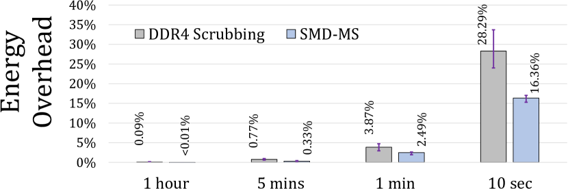
We make two observations. First, both DDR4 scrubbing and SMD-MS have negligible performance overhead for scrubbing periods of 5 minutes and larger because scrubbing operations are infrequent at such periods. Second, DDR4 scrubbing causes up to 1.49%/8.84% average slowdown for 1 minute/10 second scrubbing period (up to 2.37%/14.26%), while SMD-MS causes only up to 0.34%/1.78% slowdown. DDR4 scrubbing has high overhead at low scrubbing periods because moving data from DRAM to the MC to perform scrubbing is inefficient compared to performing scrubbing within DRAM using SMD-MS. Scrubbing at high rates may become necessary for future DRAM chips as their reliability characteristics continuously worsen. Additionally, mechanisms that improve DRAM performance at the cost of reduced reliability [124, 140] can use frequent DRAM scrubbing to achieve the desired DRAM reliability level.
We conclude that SMS performs memory scrubbing more efficiently than conventional MC based scrubbing and it enables scrubbing at high rates with small performance and energy overheads.
7.5.5 Comparison to PARA in Memory Controller
Fig. 18 compares the performance and energy overheads of PARA implemented in the MC (as proposed by Kim et al. [70]) for DDR4 and SMD-PRP for different neighbor row activation probabilities (i.e., ) across 4c-high workloads. PARA represents the performance and energy overheads with respect to conventional DDR4 with no RowHammer protection. Similarly, SMD-PRP represents the performance and energy overheads with respect to a SMD chip, which uses SMD-FR for periodic refresh, with no RowHammer protection.
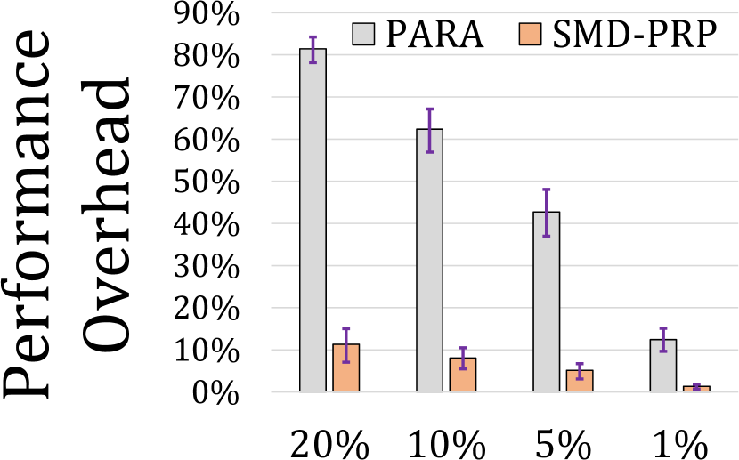
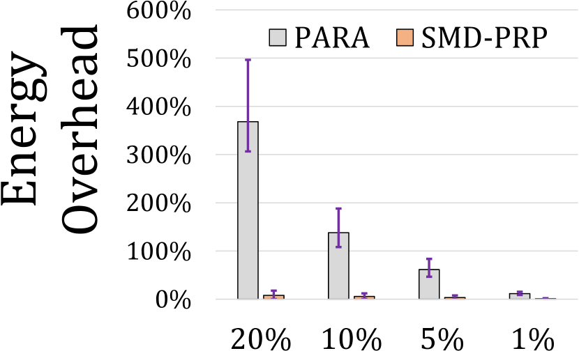
We make two observations. First, the performance and energy consumption of MC-based PARA scales poorly with . At the default of 1%, PARA incurs 12.4%/11.5% average performance/DRAM energy overhead. For higher , the overheads of PARA increase dramatically to 81.4%/368.1% at of 20%. Second, SMD-PRP is significantly more efficient than PARA. At the default of 1%, SMD-PRP incurs only 1.4%/0.9% performance/DRAM energy overheads and at of 20% the overheads become only 11.3%/8.0%. SMD-PRP is more efficient than PARA mainly due to enabling access to non-locked regions in a bank while SMD-PRP performs neighbor row refreshes on the locked region.
We conclude that SMD-PRP is a highly-efficient RowHammer protection that incurs small performance and DRAM energy overheads even with high neighbor row refresh probability, which is critical to protect future DRAM chips that may have extremely high RowHammer vulnerability.
7.5.6 SMD-DRP Maximum Activation Threshold
We analyze the SMD-DRP’s sensitivity to the maximum row activation threshold (). Fig. 19 shows the average speedup that SMD-FR and SMD-DRP achieve for different values across 4c-high workloads compared to the DDR4 baseline. When evaluating SMD-DRP, we use SMD-FR as a DRAM refresh mechanism.
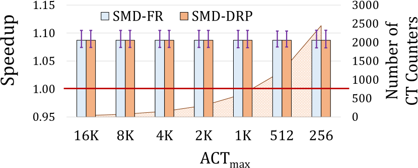
We observe that SMD-DRP incurs negligible performance overhead on top of SMD-FR even for extremely small values. This is because SMD-DRP generates very few neighbor row refreshes as 4c-high is a set of benign workloads that do not repeatedly activate a single row many times.
Although the performance overhead of SMD-DRP is negligible, the number of Counter Table (CT) entries required is significantly large for small values. For , SMD-DRP requires counters per bank, and the number of counters required increase linearly as reduces, reaching counters at the lowest that we evaluate.
7.5.7 Number of Vulnerable Neighbor Rows
We analyze the performance overheads of SMD-PRP and SMD-DRP when refreshing a different number of neighbor rows upon detecting a potentially aggressor row. Kim et al. [62] show that, in some DRAM chips, an aggressor row can cause bit flips also in rows that are at a greater distance than the two victim rows surrounding the aggressor row. Thus, it may be desirable to configure a RowHammer protection mechanism to refresh more neighbor rows than the two rows that are immediately adjacent to the aggressor row.
Fig. 20 shows the average speedup that SMD-Combined (separately with SMD-PRP and SMD-DRP) achieves for different number of neighbor rows refreshed across 4c-high workloads compared to the DDR4 baseline. The Neighbor Row Distance values on the x-axis represent the number of rows refreshes on each of the two sides of an aggressor row (e.g., for neighbor row distance of , SMD-PRP and SMD-DRP refresh four victim rows in total).
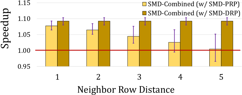
We make two key observations from the figure. First, SMD-PRP incurs large performance overheads as the neighbor row distance increases. This is because, with , SMD-PRP perform neighbor row refresh approximately for every 100th ACT command, and the latency of this refresh operation increases with the increase in the number of victim rows. Second, the performance overhead of SMD-DRP is negligible even when the neighbor row distance is five. This is because, SMD-DRP detects aggressor rows with a higher precision than SMD-PRP using area-expensive counters. As the 4c-high workloads do not repeatedly activate any single row, SMD-DRP counters rarely exceed the maximum activation threshold, and thus trigger neighbor row refresh only a few times.
7.5.8 SMD’s Performance Sensitivity to Number of Cores
The four-core workloads with high memory intensity (4c-high) largely saturate the DRAM bandwidth offered by four channels. Therefore, four cores are sufficient to capture the performance impact of SMD for cases where DRAM bandwidth utilization is high. To demonstrate this, we evaluate the performance of SMD-FR for a refresh period using highly memory-intensive 8-core (i.e., 8c-high) workloads. The speedup is comparable to the speedup of 4c-high workloads. At 32ms refresh period, SMD-FR provides 8.1% average speedup for 8c-high workloads while it provides 8.7% speedup for 4c-high workloads. SMD provides a slightly lower speedup for 8c-high because of the increased memory request queueing delay, as eight-core workloads produce more memory requests than four-core workloads.
7.6 Hardware Overhead
An SMD chip needs to transmit ACT_NACK signals to the memory controller (MC). SMD can 1) repurpose the existing alert_n pin in DDR4 chips [50, 75] or 2) introduce an extra physical pin to transmit ACT_NACK signals.
1) alert_n. alert_n is currently used to inform the MC that the DRAM chip detected a CRC or parity check failure on the issued command, and thus the MC must issue the command again. The alert_n signal can simply be asserted not only on CRC or parity check failure, but also when the MC attempts accessing a row in a locked region. This approach does not require an additional physical pin. However, assigning multiple meanings to an already ambiguous alert_n signal [50] could complicate MC design.
2) Introducing a new pin. To potentially simplify MC design, SMD can introduce a new pin to transmit ACT_NACK signals. Only one new pin between the MC and all memory devices (e.g., all DRAM chips in a memory channel or a rank) is enough for systems that use rank-based DRAM chip organizations (e.g., DDR4 DIMMs). For example, 128 new pins are needed for a high-end system with 32 memory channels equipped with 4-rank memory chips in each channel. However, a system at this scale already has 4’094 processor pins [153], and 128 new pins would amount to a relatively small 3.13% increase in pins. Similar to how alert_n signal works, the module can send the MC a single ACT_NACK when any of the per-chip ACT_NACK signals are asserted.
We individually discuss the other changes required on the existing DRAM chip and the MC circuitry.
7.6.1 DRAM Chip Modifications
We use CACTI [100] to evaluate the hardware overhead of the changes that SMD introduces over a conventional DRAM bank (highlighted in Fig. 3) assuming technology. Lock Region Table (LRT) is a small table that stores a single bit for each lock region to indicate whether or not the lock region is under maintenance. In our evaluation, we assume that a bank is divided into lock regions. Therefore, LRT consists of only bits, which are indexed using a 4-bit lock region address. According to our evaluation, an LRT incurs only area overhead per bank. The area overhead of all LRTs in a DRAM chip is only 0.001% of a DRAM chip. The access time of an LRT is , which is only 0.4% of typical row activation latency (tRCD) of .
SMD adds a per-region RA-latch to enable accessing one lock region while another is under maintenance. An RA-latch stores a pre-decoded row address, which is provided by the global row address decoder, and drives the local row decoders where the row address is fully decoded. According to our evaluation, all RA-latches incur a total area overhead of 1.63% of a DRAM chip. An RA-latch has only latency, which is negligible compared to tRCD.
Besides these changes that are the core of the SMD substrate, a particular maintenance mechanism may incur additional area overhead. We evaluate the DRAM chip area overhead of the maintenance mechanisms presented in section 5. The simple refresh mechanism, SMD-FR, requires only additional area in a DRAM chip. SMD-VR maintains bloom filters that constitute a large portion of the required . The DRAM chip area overhead of each refresh mechanism is less than 0.1% of a typical DRAM chip. SMD-PRP requires area, which is a similarly small portion of a typical DRAM chip. SMD-DRP requires a large Counter Table with 1224 counters per bank for the RowHammer threshold value that we use in our performance evaluation. Across a DRAM chip, SMD-DRP requires area, which is 7.0% of a typical DRAM chip size. The control logic of SMD-MS is similar to the control logic of SMD-FR and it requires only additional area excluding the area of the ECC engine, which is already implemented by DRAM chips that support in-DRAM ECC.
7.6.2 Memory Controller Modifications
We slightly modify the MC’s request scheduling mechanism to retry a rejected ACT command as we explain in section 4.2. Upon receiving an ACT_NACK, the MC marks the corresponding bank as precharged. An existing MC already implements control circuitry to pick an appropriate request from the request queue and issue the necessary DRAM command based on the DRAM bank state (e.g., ACT to a precharged bank or RD if the corresponding row is already open) by respecting the DRAM timing parameters. The ACT Retry Interval (ARI) is simply a new timing parameter that specifies the minimum time interval for issuing an ACT to a lock region after receiving an ACT_NACK from the same region. Therefore, SMD can be implemented in existing MCs with only slight modifications by leveraging the existing request scheduler (e.g., FRFCFS [104]).
No further changes are required in the MC to support different maintenance mechanisms enabled by SMD. Thus, SMD enables the DRAM vendors to update existing maintenance mechanisms and implement new ones without any further changes to MCs that support SMD.
8 Related Work
To our knowledge, this is the first paper to propose simple changes to existing DRAM interfaces for enabling DRAM chips that autonomously perform various maintenance operations. Our new Self-Managing DRAM (SMD) design enables implementing maintenance operations completely within DRAM without requiring further changes in the DRAM interface, Memory Controller (MC) or other system components. We briefly discuss relevant prior works.
Changing the DRAM Interface. Several prior works [148, 37, 30, 22] propose using high-speed serial links and packed-based protocols in DRAM chips. SMD differs from prior works in two key aspects. First, none of these works describe how to implement maintenance mechanisms completely within DRAM. We propose five new SMD-based maintenance mechanisms (section 5). Second, prior works significantly overhaul the existing DRAM interface, which makes their proposals more difficult to adopt compared to SMD, which adds only a single ACT_NACK signal to the existing DRAM interface and requires slight modifications in the MC.
Mitigating DRAM Refresh Overhead. Many previous works [16, 86, 124, 107, 6, 8, 23, 26, 34, 46, 55, 63, 90, 64, 87, 99, 106, 117, 145, 57, 58, 59, 150, 121, 125, 39, 68, 110, 74] propose techniques to reduce DRAM refresh overhead. SMD not only enables maintenance mechanisms for reducing DRAM refresh overhead but also other efficient maintenance mechanisms for improving DRAM reliability and security, described in section 5.
RowHammer Protection. Many prior works [82, 139, 143, 155, 116, 159, 138, 5, 20, 70, 31, 43, 149, 12, 73, 70, 155, 123, 28, 67, 69, 7] propose techniques for RowHammer protection. Although we propose SMD-PRP, SMD-PRP+, and SMD-DRP, SMD can be used to implement other existing or new RowHammer protection mechanisms.
Memory Scrubbing. Although prior works report that the overhead of memory scrubbing is small as low scrubbing rate (e.g., scrubbing period of 24 hours [141, 126, 53], 45 minutes per 1 GB scrubbing rate [132], scrubbing only when idle [94]) is generally sufficient, the cost of scrubbing can dramatically increase for future DRAM chips due to increasing DRAM bit error rate and increasing DRAM chip density. SMD-MS enables efficient scrubbing by eliminating off-chip data transfers.
Leveraging Subarray-level Parallelism. Prior works overlap the latency of accessing multiple subarrays via modifications to the DRAM architecture [71, 161, 16]. SMD’s maintenance-access parallelization builds on the basic design proposed in SALP [71] and refresh-access parallelization introduced in [16, 161]. A DDRx interface based on these prior works [71, 161, 16] still needs to change for each new maintenance operation that the DRAM manufacturer needs to implement. SMD, in contrast, allows the implementation of new maintenance mechanisms without making any further changes to the DDRx interface.
Compute Express Link (CXL) [21]. CXL is a cache-coherent interconnect for computing systems. CXL does not define the interface between a memory controller and a DRAM module/chip. Even with CXL, the memory controller chip has to deal with the management complexity of DRAM. SMD can be used in conjunction with CXL to ease management complexity in computing systems.
9 Conclusion
To set the memory controller free from managing DRAM maintenance operations, Self-Managing DRAM (SMD) introduces minimal changes to the existing DRAM chips and memory controllers. SMD enables in-DRAM maintenance operations with no further changes to the DRAM interface, memory controller, or other system components. Using SMD, we implement efficient maintenance mechanisms for DRAM refresh, RowHammer protection, and memory scrubbing. We show that these mechanisms altogether enable a higher performance, more energy efficient and at the same time more reliable and secure DRAM system. We believe and hope that SMD will enable practical adoption of innovative ideas in DRAM design.
Acknowledgments
We thank the SAFARI Research Group members for valuable feedback and the stimulating intellectual environment they provide. We acknowledge the generous gifts provided by our industrial partners, including Google, Huawei, Intel, Microsoft, and VMware, and support from the Microsoft Swiss Joint Research Center.
References
- [1] DRAM Circuit Design: Fundamental and High-Speed Topics.
- [2] “DRAMPower Source Code,” https://github.com/tukl-msd/DRAMPower.
- [3] Apple Inc., “About the Security Content of Mac EFI Security Update 2015-001,” https://support.apple.com/en-us/HT204934, 2015.
- [4] M. Awasthi, M. Shevgoor, K. Sudan, B. Rajendran, R. Balasubramonian, and V. Srinivasan, “Efficient Scrub Mechanisms for Error-Prone Emerging Memories,” in HPCA, 2012.
- [5] Z. B. Aweke, S. F. Yitbarek, R. Qiao, R. Das, M. Hicks, Y. Oren, and T. Austin, “ANVIL: Software-Based Protection Against Next-Generation Rowhammer Attacks,” in ASPLOS, 2016.
- [6] S. Baek, S. Cho, and R. Melhem, “Refresh Now and Then,” in TC, 2014.
- [7] T. Bennett et al., “Panopticon: A Complete In-DRAM Rowhammer Mitigation,” in Workshop on DRAM Security (DRAMSec), 2021.
- [8] I. Bhati, Z. Chishti, and B. Jacob, “Coordinated Refresh: Energy Efficient Techniques for DRAM Refresh Scheduling,” in ISPLED, 2013.
- [9] I. Bhati, Z. Chishti, S.-L. Lu, and B. Jacob, “Flexible Auto-Refresh: Enabling Scalable and Energy-Efficient DRAM Refresh Reductions,” in ISCA, 2015.
- [10] B. H. Bloom, “Space/Time Trade-offs in Hash Coding with Allowable Errors,” Communications of the ACM, 1970.
- [11] F. N. Bostancı, A. Olgun, L. Orosa, A. G. Yağlıkçı, J. S. Kim, H. Hassan, O. Ergin, and O. Mutlu, “DR-STRaNGe: End-to-End System Design for DRAM-based True Random Number Generators,” in HPCA, 2022.
- [12] F. Brasser, L. Davi, D. Gens, C. Liebchen, and A.-R. Sadeghi, “Can’t Touch This: Practical and Generic Software-only Defenses Against RowHammer Attacks,” USENIX Security, 2017.
- [13] S. Cha, O. Seongil, H. Shin, S. Hwang, K. Park, S. J. Jang, J. S. Choi, G. Y. Jin, Y. H. Son, H. Cho, J. H. Ahn, and N. S. Kim, “Defect Analysis and Cost-Effective Resilience Architecture for Future DRAM Devices,” in HPCA, 2017.
- [14] K. Chandrasekar, B. Akesson, and K. Goossens, “Improved Power Modeling of DDR SDRAMs,” in DSD, 2011.
- [15] K. K. Chang, A. Kashyap, H. Hassan, S. Ghose, K. Hsieh, D. Lee, T. Li, G. Pekhimenko, S. Khan, and O. Mutlu, “Understanding Latency Variation in Modern DRAM Chips: Experimental Characterization, Analysis, and Optimization,” in SIGMETRICS, 2016.
- [16] K. K. Chang, D. Lee, Z. Chishti, A. R. Alameldeen, C. Wilkerson, Y. Kim, and O. Mutlu, “Improving DRAM Performance by Parallelizing Refreshes with Accesses,” in HPCA, 2014.
- [17] K. K. Chang, P. J. Nair, D. Lee, S. Ghose, M. K. Qureshi, and O. Mutlu, “Low-Cost Inter-Linked Subarrays (LISA): Enabling Fast Inter-Subarray Data Movement in DRAM,” in HPCA, 2016.
- [18] K. K. Chang, A. G. Yağlikçi, S. Ghose, A. Agrawal, N. Chatterjee, A. Kashyap, D. Lee, M. O’Connor, H. Hassan, and O. Mutlu, “Understanding Reduced-Voltage Operation in Modern DRAM Devices: Experimental Characterization, Analysis, and Mechanisms,” in SIGMETRICS, 2017.
- [19] L. Cojocar, J. Kim, M. Patel, L. Tsai, S. Saroiu, A. Wolman, and O. Mutlu, “Are We Susceptible to Rowhammer? An End-to-End Methodology for Cloud Providers,” S&P, 2020.
- [20] L. Cojocar, K. Razavi, C. Giuffrida, and H. Bos, “Exploiting Correcting Codes: On the Effectiveness of ECC Memory Against RowHammer Attacks,” in S&P, 2019.
- [21] COMPUTE EXPRESS LINK CONSORTIUM, Compute Express Link (CXL) - Specification, 2022.
- [22] E. Cooper-Balis, P. Rosenfeld, and B. Jacob, “Buffer-on-Board Memory Systems,” in ISCA, 2012.
- [23] Z. Cui, S. A. McKee, Z. Zha, Y. Bao, and M. Chen, “DTail: A Flexible Approach to DRAM Refresh Management,” in SC, 2014.
- [24] F. de Ridder, P. Frigo, E. Vannacci, H. Bos, C. Giuffrida, and K. Razavi, “SMASH: Synchronized Many-sided Rowhammer Attacks from JavaScript,” in USENIX Security, 2021.
- [25] T. J. Dell, “A White Paper on the Benefits of Chipkill-Correct ECC for PC Server Main Memory,” IBM Microelectronics Division, 1997.
- [26] P. G. Emma, W. R. Reohr, and M. Meterelliyoz, “Rethinking Refresh: Increasing Availability and Reducing Power in DRAM for Cache Applications,” in MICRO, 2008.
- [27] S. Eyerman and L. Eeckhout, “System-level Performance Metrics for Multiprogram Workloads,” in IEEE Micro, 2008.
- [28] A. Fakhrzadehgan, Y. N. Patt, P. J. Nair, and M. K. Qureshi, “SafeGuard: Reducing the Security Risk from Row-Hammer via Low-Cost Integrity Protection,” in HPCA, 2022.
- [29] L. Fan, P. Cao, J. Almeida, and A. Z. Broder, “Summary Cache: A Scalable Wide-Area Web Cache Sharing Protocol,” SIGCOMM, 1998.
- [30] K. Fang, L. Chen, Z. Zhang, and Z. Zhu, “Memory Architecture for Integrating Emerging Memory Technologies,” in PACT, 2011.
- [31] P. Frigo, E. Vannacci, H. Hassan, V. van der Veen, O. Mutlu, C. Giuffrida, H. Bos, and K. Razavi, “TRRespass: Exploiting the Many Sides of Target Row Refresh,” in SP, 2020.
- [32] J. E. Fritts, F. W. Steiling, and J. A. Tucek, “Mediabench II Video: Expediting the Next Generation of Video Systems Research,” in Electronic Imaging, 2005.
- [33] S. Gautam, S. Manhas, A. Kumar, M. Pakala, and E. Yieh, “Row Hammering Mitigation Using Metal Nanowire in Saddle Fin DRAM,” TED, 2019.
- [34] M. Ghosh and H.-H. S. Lee, “Smart Refresh: An Enhanced Memory Controller Design for Reducing Energy in Conventional and 3D Die-stacked DRAMs,” in MICRO, 2007.
- [35] S.-L. Gong, J. Kim, S. Lym, M. Sullivan, H. David, and M. Erez, “DUO: Exposing on-chip Redundancy to Rank-level ECC for High Reliability,” in HPCA, 2018.
- [36] Z. Greenfield and L. Tomer, “Throttling Support for Row-Hammer Counters,” 2016, US Patent 9,251,885.
- [37] T. J. Ham, B. K. Chelepalli, N. Xue, and B. C. Lee, “Disintegrated Control for Energy-Efficient and Heterogeneous Memory Systems,” in HPCA, 2013.
- [38] R. W. Hamming, “Error Detecting and Error Correcting Codes,” in Bell Labs Technical Journal, 1950.
- [39] H. Hassan, M. Patel, J. S. Kim, A. G. Yağlıkçı, N. Vijaykumar, N. M. Ghiasi, S. Ghose, and O. Mutlu, “CROW: A Low-Cost Substrate for Improving DRAM Performance, Energy Efficiency, and Reliability,” in ISCA, 2019.
- [40] H. Hassan, G. Pekhimenko, N. Vijaykumar, V. Seshadri, D. Lee, O. Ergin, and O. Mutlu, “ChargeCache: Reducing DRAM Latency by Exploiting Row Access Locality,” in HPCA, 2016.
- [41] H. Hassan, Y. C. Tugrul, J. S. Kim, V. Van der Veen, K. Razavi, and O. Mutlu, “Uncovering In-DRAM RowHammer Protection Mechanisms: A New Methodology, Custom RowHammer Patterns, and Implications,” in MICRO, 2021.
- [42] H. Hassan, N. Vijaykumar, S. Khan, S. Ghose, K. Chang, G. Pekhimenko, D. Lee, O. Ergin, and O. Mutlu, “SoftMC: A Flexible and Practical Open-Source Infrastructure for Enabling Experimental DRAM Studies,” in HPCA, 2017.
- [43] N. Herath and Anders Fogh, “These are Not Your Grand Daddy’s CPU Performance Counters,” in Black Hat Briefings, 2015.
- [44] S. Hong, “Memory Technology Trend and Future Challenges,” in IEDM, 2010.
- [45] S. Hynix, “DDR4 SDRAM Device Operation.”
- [46] C. Isen and L. John, “ESKIMO: Energy Savings Using Semantic Knowledge of Inconsequential Memory Occupancy for DRAM Subsystem,” in MICRO, 2009.
- [47] B. Jacob, D. Wang, and S. Ng, Memory Systems: Cache, DRAM, Disk. Morgan Kaufmann, 2010.
- [48] P. Jattke, V. van der Veen, P. Frigo, S. Gunter, and K. Razavi, “Blacksmith: Scalable Rowhammering in the Frequency Domain,” in S&P, 2022.
- [49] JEDEC, DDR3 SDRAM Specification, 2008.
- [50] JEDEC, “Double Data Rate 4 (DDR4) SDRAM Standard,” 2012.
- [51] JEDEC, “Low Power Double Data Rate 4 (LPDDR4) SDRAM Specification,” 2014.
- [52] JEDEC, “LPDDR5 SDRAM Specification - JESD209-5,” 2019.
- [53] JEDEC, “DDR5 SDRAM Specification - JESD79-5A,” 2021.
- [54] Y. Jiang, H. Zhu, D. Sullivan, X. Guo, X. Zhang, and Y. Jin, “Quantifying Rowhammer Vulnerability for DRAM Security,” in DAC, 2021.
- [55] M. Jung, É. Zulian, D. M. Mathew, M. Herrmann, C. Brugger, C. Weis, and N. Wehn, “Omitting Refresh: A Case Study for Commodity and Wide I/O DRAMs,” in MEMSYS, 2015.
- [56] U. Kang, H. S. Yu, C. Park, H. Zheng, J. Halbert, K. Bains, S. Jang, and J. S. Choi, “Co-Architecting Controllers and DRAM to Enhance DRAM Process Scaling,” in The Memory Forum, 2014.
- [57] S. Khan, D. Lee, Y. Kim, A. R. Alameldeen, C. Wilkerson, and O. Mutlu, “The Efficacy of Error Mitigation Techniques for DRAM Retention Failures: A Comparative Experimental Study,” in SIGMETRICS, 2014.
- [58] S. Khan, D. Lee, and O. Mutlu, “PARBOR: An Efficient System-Level Technique to Detect Data-Dependent Failures in DRAM,” in DSN, 2016.
- [59] S. Khan, C. Wilkerson, Z. Wang, A. R. Alameldeen, D. Lee, and O. Mutlu, “Detecting and Mitigating Data-Dependent DRAM Failures by Exploiting Current Memory Content,” in MICRO, 2017.
- [60] J. S. Kim, M. Patel, H. Hassan, and O. Mutlu, “The DRAM Latency PUF: Quickly Evaluating Physical Unclonable Functions by Exploiting the Latency-Reliability Tradeoff in Modern Commodity DRAM Devices,” in HPCA, 2018.
- [61] J. S. Kim, M. Patel, H. Hassan, L. Orosa, and O. Mutlu, “D-RaNGe: Using Commodity DRAM Devices to Generate True Random Numbers with Low Latency and High Throughput,” in HPCA, 2019.
- [62] J. S. Kim, M. Patel, A. G. Yaglikci, H. Hassan, R. Azizi, L. Orosa, and O. Mutlu, “Revisiting RowHammer: An Experimental Analysis of Modern DRAM Devices and Mitigation Techniques,” in ISCA, 2020.
- [63] J. Kim and M. C. Papaefthymiou, “Dynamic Memory Design for Low Data-Retention Power,” in PATMOS, 2000.
- [64] J. Kim and M. C. Papaefthymiou, “Block-Based Multiperiod Dynamic Memory Design for Low Data-Retention Power,” in TVLSI, 2003.
- [65] K. Kim and J. Lee, “A New Investigation of Data Retention Time in Truly Nanoscaled DRAMs,” in EDL, 2009.
- [66] M. J. Kim, J. Park, Y. Park, W. Doh, N. Kim, T. J. Ham, J. W. Lee, and J. H. Ahn, “Mithril: Cooperative Row Hammer Protection on Commodity DRAM Leveraging Managed Refresh,” arXiv preprint arXiv:2108.06703, 2021.
- [67] M. J. Kim, J. Park, Y. Park, W. Doh, N. Kim, T. J. Ham, J. W. Lee, and J. H. Ahn, “Mithril: Cooperative row hammer protection on commodity dram leveraging managed refresh,” in HPCA, 2022.
- [68] S. Kim, W. Kwak, C. Kim, D. Baek, and J. Huh, “Charge-Aware DRAM Refresh Reduction with Value Transformation,” in HPCA, 2020.
- [69] W. Kim, C. Jung, S. Yoo, D. Hong, J. Hwang, J. Yoon, O. Jung, J. Choi, S. Hyun, M. Kang et al., “A 1.1 V 16Gb DDR5 DRAM with Probabilistic-Aggressor Tracking, Refresh-Management Functionality, Per-Row Hammer Tracking, a Multi-Step Precharge, and Core-Bias Modulation for Security and Reliability Enhancement,” in ISSCC. IEEE, 2023.
- [70] Y. Kim, R. Daly, J. Kim, C. Fallin, J. H. Lee, D. Lee, C. Wilkerson, K. Lai, and O. Mutlu, “Flipping Bits in Memory Without Accessing Them: An Experimental Study of DRAM Disturbance Errors,” in ISCA, 2014.
- [71] Y. Kim, V. Seshadri, D. Lee, J. Liu, and O. Mutlu, “A Case for Exploiting Subarray-level Parallelism (SALP) in DRAM,” in ISCA, 2012.
- [72] Y. Kim, W. Yang, and O. Mutlu, “Ramulator: A Fast and Extensible DRAM Simulator,” in CAL, 2015.
- [73] R. K. Konoth, M. Oliverio, A. Tatar, D. Andriesse, H. Bos, C. Giuffrida, and K. Razavi, “ZebRAM: Comprehensive and Compatible Software Protection Against Rowhammer Attacks,” in OSDI, 2018.
- [74] H. Kwon, K. Kim, D. Jeon, and K.-S. Chung, “Reducing Refresh Overhead with In-DRAM Error Correction Codes,” in ISOCC, 2021.
- [75] S. Kwon, Y. H. Son, and J. H. Ahn, “Understanding DDR4 in Pursuit of in-DRAM ECC,” in ISOCC, 2014.
- [76] D. Lee, Y. Kim, G. Pekhimenko, S. Khan, V. Seshadri, K. Chang, and O. Mutlu, “Adaptive-Latency DRAM: Optimizing DRAM Timing for the Common-Case,” in HPCA, 2015.
- [77] D. Lee, S. Ghose, G. Pekhimenko, S. Khan, and O. Mutlu, “Simultaneous Multi-Layer Access: Improving 3D-Stacked Memory Bandwidth at Low Cost,” in TACO, 2016.
- [78] D. Lee, S. Khan, L. Subramanian, S. Ghose, R. Ausavarungnirun, G. Pekhimenko, V. Seshadri, and O. Mutlu, “Design-Induced Latency Variation in Modern DRAM Chips: Characterization, Analysis, and Latency Reduction Mechanisms,” in SIGMETRICS, 2017.
- [79] D. Lee, Y. Kim, V. Seshadri, J. Liu, L. Subramanian, and O. Mutlu, “Tiered-Latency DRAM: A Low Latency and Low Cost DRAM Architecture,” in HPCA, 2013.
- [80] D. Lee, L. Subramanian, R. Ausavarungnirun, J. Choi, and O. Mutlu, “Decoupled Direct Memory Access: Isolating CPU and IO Traffic by Leveraging a Dual-Data-Port DRAM,” in PACT, 2015.
- [81] E. Lee, I. Kang, S. Lee, G. Edward Suh, and J. Ho Ahn, “TWiCe: Preventing Row-Hammering by Exploiting Time Window Counters,” in ISCA, 2019.
- [82] E. Lee, S. Lee, G. E. Suh, and J. H. Ahn, “TWiCe: Time Window Counter Based Row Refresh to Prevent Row-Hammering,” CAL, 2018.
- [83] S.-H. Lee, “Technology Scaling Challenges and Opportunities of Memory Devices,” in IEDM, 2016.
- [84] Y. Li, H. Schneider, F. Schnabel, R. Thewes, and D. Schmitt-Landsiedel, “DRAM Yield Analysis and Optimization by a Statistical Design Approach,” in CSI, 2011.
- [85] J. Liu, B. Jaiyen, Y. Kim, C. Wilkerson, and O. Mutlu, “An Experimental Study of Data Retention Behavior in Modern DRAM Devices: Implications for Retention Time Profiling Mechanisms,” in ISCA, 2013.
- [86] J. Liu, B. Jaiyen, R. Veras, and O. Mutlu, “RAIDR: Retention-Aware Intelligent DRAM Refresh,” in ISCA, 2012.
- [87] S. Liu, K. Pattabiraman, T. Moscibroda, and B. G. Zorn, “Flikker: Saving DRAM Refresh-Power Through Critical Data Partitioning,” in ASPLOS, 2012.
- [88] C.-K. Luk, R. Cohn, R. Muth, H. Patil, A. Klauser, G. Lowney, S. Wallace, V. J. Reddi, and K. Hazelwood, “Pin: Building Customized Program Analysis Tools with Dynamic Instrumentation,” in PLDI, 2005.
- [89] H. Luo, T. Shahroodi, H. Hassan, M. Patel, A. G. Yağlıkçı, L. Orosa, J. Park, and O. Mutlu, “Clr-dram: A low-cost dram architecture enabling dynamic capacity-latency trade-off,” in Proceedings of the ACM/IEEE 47th Annual International Symposium on Computer Architecture, 2020.
- [90] Y. Luo, S. Govindan, B. Sharma, M. Santaniello, J. Meza, A. Kansal, J. Liu, B. Khessib, K. Vaid, and O. Mutlu, “Characterizing Application Memory Error Vulnerability to Optimize Datacenter Cost via Heterogeneous-reliability Memory,” in DSN, 2014.
- [91] J. A. Mandelman, R. H. Dennard, G. B. Bronner, J. K. DeBrosse, R. Divakaruni, Y. Li, and C. J. Radens, “Challenges and Future Directions for the Scaling of Dynamic Random-access Memory (DRAM),” in IBM JRD, 2002.
- [92] M. Marazzi, P. Jattke, S. Flavien, and K. Razavi, “PROTRR: Principled yet Optimal In-DRAM Target Row Refresh,” in S&P, 2022.
- [93] J. D. McCalpin, “STREAM: Sustainable Memory Bandwidth in High Performance Computers,” https://www.cs.virginia.edu/stream/.
- [94] J. Meza, Q. Wu, S. Kumar, and O. Mutlu, “Revisiting Memory Errors in Large-scale Production Data Centers: Analysis and Modeling of New Trends from the Field,” in DSN, 2015.
- [95] P. Michaud, “Demystifying Multicore Throughput Metrics,” CAL, 2012.
- [96] Micron, “DDDR4 SDRAM Datasheet,” 2016.
- [97] J. Misra and D. Gries, “Finding Repeated Elements,” Science of Computer Programming, 1982.
- [98] S. S. Mukherjee, J. Emer, T. Fossum, and S. K. Reinhardt, “Cache Scrubbing in Microprocessors: Myth or Necessity?” in SDC, 2004.
- [99] J. Mukundan, H. Hunter, K.-h. Kim, J. Stuecheli, and J. F. Martínez, “Understanding and Mitigating Refresh Overheads in High-density DDR4 DRAM Systems,” in ISCA, 2013.
- [100] N. Muralimanohar, R. Balasubramonian, and N. P. Jouppi, “CACTI 6.0: A Tool to Model Large Caches,” HP Laboratories, Tech. Rep. HPL-2009-85, 2009.
- [101] O. Mutlu, “Memory Scaling: A Systems Architecture Perspective,” in IMW, 2013.
- [102] O. Mutlu, “The RowHammer Problem and Other Issues We may Face as Memory Becomes Denser,” in DATE, 2017.
- [103] O. Mutlu and J. S. Kim, “RowHammer: A Retrospective,” TCAD, 2019.
- [104] O. Mutlu and T. Moscibroda, “Stall-Time Fair Memory Access Scheduling for Chip Multiprocessors,” in MICRO, 2007.
- [105] O. Mutlu and L. Subramanian, “Research Problems and Opportunities in Memory Systems,” in SUPERFRI, 2014.
- [106] P. Nair, C.-C. Chou, and M. K. Qureshi, “A Case for Refresh Pausing in DRAM Memory Systems,” in HPCA, 2013.
- [107] P. J. Nair, C.-C. Chou, and M. K. Qureshi, “Refresh Pausing in DRAM Memory Systems,” in TACO, 2014.
- [108] P. J. Nair, D.-H. Kim, and M. K. Qureshi, “ArchShield: Architectural Framework for Assisting DRAM Scaling by Tolerating High Error Rates,” in ISCA, 2013.
- [109] P. J. Nair, V. Sridharan, and M. K. Qureshi, “XED: Exposing On-Die Error Detection Information for Strong Memory Reliability,” in ISCA, 2016.
- [110] K. Nguyen, K. Lyu, X. Meng, V. Sridharan, and X. Jian, “Nonblocking Memory Refresh,” in ISCA, 2018.
- [111] A. Olgun, M. Patel, A. G. Yağlıkçı, H. Luo, J. S. Kim, F. N. Bostancı, N. Vijaykumar, O. Ergin, and O. Mutlu, “QUAC-TRNG: High-Throughput True Random Number Generation Using Quadruple Row Activation in Commodity DRAM Chips,” in ISCA, 2021.
- [112] L. Orosa, A. G. Yaglikci, H. Luo, A. Olgun, J. Park, H. Hassan, M. Patel, J. S. Kim, and O. Mutlu, “A Deeper Look into RowHammer’s Sensitivities: Experimental Analysis of Real DRAM Chips and Implications on Future Attacks and Defenses,” in MICRO, 2021.
- [113] K. Park, C. Lim, D. Yun, and S. Baeg, “Experiments and Root Cause Analysis for Active-Precharge Hammering Fault in DDR3 SDRAM under 3 nm Technology,” in Microelectronics Reliability, 2016.
- [114] K. Park, D. Yun, and S. Baeg, “Statistical Distributions of Row-Hammering Induced Failures in DDR3 Components,” in Microelectronics Reliability, 2016.
- [115] S.-K. Park, “Technology Scaling Challenge and Future Prospects of DRAM and NAND Flash Memory,” in IMW, 2015.
- [116] Y. Park, W. Kwon, E. Lee, T. J. Ham, J. H. Ahn, and J. Lee, “Graphene: Strong yet lightweight row hammer protection,” in MICRO, 2020.
- [117] K. Patel, L. Benini, E. Macii, and M. Poncino, “Energy-Efficient Value-based Selective Refresh for Embedded DRAMs,” in PATMOS, 2005.
- [118] M. Patel, G. F. de Oliveira, and O. Mutlu, “HARP: Practically and Effectively Identifying Uncorrectable Errors in Memory Chips That Use On-Die Error-Correcting Codes,” in MICRO, 2021.
- [119] M. Patel, J. Kim, T.-M. Shahroodi, H. Hassan, and O. Mutlu, “Bit-Exact ECC Recovery (BEER): Determining DRAM On-Die ECC Functions by Exploiting DRAM Data Retention Characteristics,” in MICRO, 2020.
- [120] M. Patel, J. S. Kim, H. Hassan, and O. Mutlu, “Understanding and Modeling On-Die Error Correction in Modern DRAM: An Experimental Study Using Real Devices,” in DSN, 2019.
- [121] M. Patel, J. S. Kim, and O. Mutlu, “The Reach Profiler (REAPER): Enabling the Mitigation of DRAM Retention Failures via Profiling at Aggressive Conditions,” in ISCA, 2017.
- [122] S. Pontarelli, P. Reviriego, and J. A. Maestro, “Improving Counting Bloom Filter Performance with Fingerprints,” Information Processing Letters, 2016.
- [123] M. Qureshi, A. Rohan, G. Saileshwar, and P. J. Nair, “Hydra: Enabling Low-Overhead Mitigation of Row-Hammer at Ultra-Low Thresholds via Hybrid Tracking,” in ISCA, 2022.
- [124] M. K. Qureshi, D. Kim, S. Khan, P. J. Nair, and O. Mutlu, “AVATAR: A Variable-Retention-Time (VRT) Aware Refresh for DRAM Systems,” in DSN, 2015.
- [125] Y. Riho and K. Nakazato, “Partial Access Mode: New Method for Reducing Power Consumption of Dynamic Random Access Memory,” 2014.
- [126] R. Rooney and N. Koyle, “Micron DDR5 SDRAM: New Features,” Micron Technology Inc., Tech. Rep, 2019.
- [127] S.-W. Ryu, K. Min, J. Shin, H. Kwon, D. Nam, T. Oh, T.-S. Jang, M. Yoo, Y. Kim, and S. Hong, “Overcoming the Reliability Limitation in the Ultimately Scaled DRAM using Silicon Migration Technique by Hydrogen Annealing,” in IEDM, 2017.
- [128] SAFARI Research Group, “Ramulator Source Code,” https://github.com/CMU-SAFARI/ramulator.
- [129] G. Saileshwar, B. Wang, M. Qureshi, and P. J. Nair, “Randomized Row-Swap: Mitigating Row Hammer by Breaking Spatial Correlation between Aggressor and Victim Rows,” in ASPLOS, 2022.
- [130] K. Saino, S. Horiba, S. Uchiyama, Y. Takaishi, M. Takenaka, T. Uchida, Y. Takada, K. Koyama, H. Miyake, and C. Hu, “Impact of Gate-induced Drain Leakage Current on the Tail Distribution of DRAM Data Retention Time,” in IEDM, 2000.
- [131] A. M. Saleh, J. J. Serrano, and J. H. Patel, “Reliability of Scrubbing Recovery-Techniques for Memory Systems,” IEEE Transactions on Reliability, 1990.
- [132] B. Schroeder, E. Pinheiro, and W.-D. Weber, “DRAM Errors in the Wild: a Large-scale Field Study,” in SIGMETRICS, 2009.
- [133] Self-Managing DRAM (SMD) Source Code, https://github.com/CMU-SAFARI/SelfManagingDRAM.
- [134] V. Seshadri, Y. Kim, C. Fallin, D. Lee, R. Ausavarungnirun, G. Pekhimenko, Y. Luo, O. Mutlu, P. B. Gibbons, M. A. Kozuch, and T. Mowry, “RowClone: Fast and Energy-Efficient In-DRAM Bulk Data Copy and Initialization,” in MICRO, 2013.
- [135] V. Seshadri, D. Lee, T. Mullins, H. Hassan, A. Boroumand, J. Kim, M. A. Kozuch, O. Mutlu, P. B. Gibbons, and T. C. Mowry, “Ambit: In-Memory Accelerator for Bulk Bitwise Operations Using Commodity DRAM Technology,” in MICRO, 2017.
- [136] V. Seshadri, T. Mullins, A. Boroumand, O. Mutlu, P. B. Gibbons, M. A. Kozuch, and T. C. Mowry, “Gather-scatter DRAM: In-DRAM Address Translation to Improve the Spatial Locality of Non-unit Strided Accesses,” in MICRO, 2015.
- [137] V. Seshadri and O. Mutlu, “In-DRAM Bulk Bitwise Execution Engine,” Advances in Computers, 2020.
- [138] S. M. Seyedzadeh, A. K. Jones, and R. Melhem, “Mitigating Wordline Crosstalk Using Adaptive Trees of Counters,” in ISCA, 2018.
- [139] S. M. Seyedzadeh, A. K. Jones, and R. Melhem, “Counter-based Tree Structure for Row Hammering Mitigation in DRAM,” CAL, 2017.
- [140] R. Sharifi and Z. Navabi, “Online Profiling for Cluster-Specific Variable Rate Refreshing in High-Density DRAM Systems,” in ETS, 2017.
- [141] T. Siddiqua, V. Sridharan, S. E. Raasch, N. DeBardeleben, K. B. Ferreira, S. Levy, E. Baseman, and Q. Guan, “Lifetime Memory Reliability Data from the Field,” in DFT, 2017.
- [142] A. Snavely and D. M. Tullsen, “Symbiotic Jobscheduling for a Simultaneous Mutlithreading Processor,” in ASPLOS, 2000.
- [143] M. Son, H. Park, J. Ahn, and S. Yoo, “Making DRAM Stronger Against Row Hammering,” in DAC, 2017.
- [144] Standard Performance Evaluation Corp., “SPEC CPU@2006,” 2006, http://www.spec.org/cpu2006.
- [145] J. Stuecheli, D. Kaseridis, H. C. Hunter, and L. K. John, “Elastic Refresh: Techniques to Mitigate Refresh Penalties in High Density Memory,” in MICRO, 2010.
- [146] M. Taouil, C. Reinbrecht, S. Hamdioui, and J. Sepúlveda, “LightRoAD: Lightweight Rowhammer Attack Detector,” in ISVLSI, 2021.
- [147] Transaction Processing Performance Council, “TPC Benchmarks,” http://www.tpc.org/.
- [148] A. N. Udipi, N. Muralimanohar, R. Balasubramonian, A. Davis, and N. P. Jouppi, “Combining Memory and a Controller with Photonics Through 3D-Stacking to Enable Scalable and Energy-Efficient Systems,” in ISCA, 2011.
- [149] V. van der Veen, M. Lindorfer, Y. Fratantonio, H. P. Pillai, G. Vigna, C. Kruegel, H. Bos, and K. Razavi, “GuardION: Practical Mitigation of DMA-Based Rowhammer Attacks on ARM,” in DIMVA, 2018.
- [150] R. K. Venkatesan, S. Herr, and E. Rotenberg, “Retention-Aware Placement in DRAM (RAPID): Software Methods for Quasi-Non-Volatile DRAM,” in HPCA, 2006.
- [151] A. J. Walker, S. Lee, and D. Beery, “On DRAM Rowhammer and the Physics of Insecurity,” TED, 2021.
- [152] Y. Wang, L. Orosa, X. Peng, Y. Guo, S. Ghose, M. Patel, J. Kim, J. Gómez-Luna, M. Sadrosadati, N. Ghiasi, and O. Mutlu, “Figaro: Improving system performance via fine-grained in-dram data relocation and caching,” in MICRO, 2020.
- [153] Wikichip, “Socket SP3 - Packages - AMD,” https://en.wikichip.org/wiki/amd/packages/socket_sp3#Pin_Map, 2022.
- [154] A. G. Yağlıkçı, H. Luo, G. F. de Oliviera, A. Olgun, M. Patel, J. Park, H. Hassan, J. S. Kim, L. Orosa, and O. Mutlu, “Understanding RowHammer Under Reduced Wordline Voltage: An Experimental Study Using Real DRAM Devices,” in DSN, 2022.
- [155] A. G. Yağlikçi, M. Patel, J. Kim, R. Azizi, A. Olgun, L. Orosa, H. Hassan, J. Park, K. Kanellopoulos, T. Shahroodi, S. Ghose, and O. Mutlu, “Blockhammer: Preventing rowhammer at low cost by blacklisting rapidly-accessed dram rows,” ArXiv, 2021.
- [156] A. G. Yağlıkçı, J. S. Kim, F. Devaux, and O. Mutlu, “Security Analysis of the Silver Bullet Technique for RowHammer Prevention,” arXiv preprint arXiv:2106.07084, 2021.
- [157] C.-M. Yang, C.-K. Wei, Y. J. Chang, T.-C. Wu, H.-P. Chen, and C.-S. Lai, “Suppression of Row Hammer Effect by Doping Profile Modification in Saddle-Fin Array Devices for sub-30-nm DRAM Technology,” TDMR, 2016.
- [158] T. Yang and X.-W. Lin, “Trap-Assisted DRAM Row Hammer Effect,” EDL, 2019.
- [159] J. M. You and J.-S. Yang, “MRLoc: Mitigating Row-Hammering Based on Memory Locality,” in DAC, 2019.
- [160] T. Zhang, K. Chen, C. Xu, G. Sun, T. Wang, and Y. Xie, “Half-DRAM: A High-Bandwidth and Low-Power DRAM Architecture from the Rethinking of Fine-Grained Activation,” in ISCA, 2014.
- [161] T. Zhang, M. Poremba, C. Xu, G. Sun, and Y. Xie, “CREAM: A Concurrent-Refresh-Aware DRAM Memory Architecture,” in HPCA, 2014.
- [162] X. Zhang, Y. Zhang, B. R. Childers, and J. Yang, “Restore Truncation for Performance Improvement in Future DRAM Systems,” in HPCA, 2016.