Hysteresis-Free High Mobility Graphene Encapsulated in Tungsten Disulfide
Abstract
High mobility is a crucial requirement for a large variety of electronic device applications. The state-of-the-art for high quality graphene devices is based on heterostructures made with graphene encapsulated in nm-thick flakes of hexagonal boron nitride (hBN). Unfortunately, scaling up multilayer hBN while precisely controlling the number of layers remains an elusive challenge, resulting in a rough material unable to enhance the mobility of graphene. This leads to the pursuit of alternative, scalable materials, which can be simultaneously used as substrate and encapsulant for graphene. Tungsten disulfide (WS2) is a transition metal dichalcogenide, which was successfully grown in large (mm-size) multi-layers by chemical vapour deposition. However, the resistance vs gate voltage characteristics when gating graphene through WS2 exhibit largely hysteretic shifts of the charge neutrality point (CNP) in the order of 2.61011 cm-2, hindering the use of WS2 as a reliable encapsulant. The hysteresis originates due to the charge traps from sulfur vacancies present in WS2. In this work, we report for the first time the use of WS2 as a substrate and the overcoming of hysteresis issues by chemically treating WS2 with a super-acid, which passivates these vacancies and strips the surface from contaminants. The hysteresis is significantly reduced below the noise level by at least a factor five (to 51010 cm-2) and, simultaneously, the room-temperature mobility of WS2-encapsulated graphene is as high as 6.2104 cm-2V-1s-1 at a carrier density 1 cm-2. Our results promote WS2 to a valid alternative to hBN as encapsulant for high-performance graphene devices.
High mobility is a crucial requirement for multiple electronic and optoelectronic applications such as field effect transistors[1], modulators[2], photodetectors[3, 4] and sensors[5]. Owing to its ultra-high (105 cm-2V-1s-1) room-temperature mobility[6], complemented by broadband absorption[7], scalability[8, 9] and compatibility to the complementary metal-oxide-semiconductor (CMOS) platform[10], graphene is quickly rising for consideration in advanced multi-purpose technologies[11, 2]. The room-temperature mobility in graphene is limited by the scattering of carriers with acoustic phonons[12] and it is typically inversely proportional to the residual charge carrier density (*)[13], which arises from local strain fluctuations in graphene[13, 14]. In this context, the choice of the perfect substrate, dictated by the need of atomic flatness and absence of charge traps, plays a vital role for preserving the extra-ordinary properties of graphene[15].
Suspended graphene exhibits extremely high mobility (2105 cm-2V-1s-1)[16] but the integration of such devices is impractical[17]. Several substrates such as aluminium dioxide (Al2O3)[18], aluminium nitride (AlN)[19], fused silica[20], strontium titanate (SrTiO3)[21] and calcium fluoride (CaF2)[22] were tested to preserve the properties of suspended graphene. Nevertheless, hexagonal boron nitride (hBN), an atomically flat, layered dielectric material is so far the unrivalled choice for encapsulating graphene[23]. State-of-the-art (SOTA) high-quality graphene (Gr) devices are encapsulated with hBN flakes and assembled through a novel stamping and cleaning technique[24]. The highest values of mobility measured in such hBN/Gr/hBN heterostructure at room temperature exceeds 105 cm2V-1s-1 at a carrier density of 1012 cm-2 with a * of 109 cm-2 [24, 25]. In such experiments atomically-flat multilayer flakes of hBN nm-thick were used both as a substrate and as a capping layer, in order to completely screen charge traps and roughness from the substrate underneath, but also to protect graphene from exposure to air-contaminants[24]. However, growing multilayer hBN films with equal flatness to the exfoliated counterpart, and being able to precisely control the number of layers, remains an open challenge[26, 27]. Additionally, hBN grown by chemical vapour deposition (CVD) tends to possess a high concentration of point defects, wrinkles and grain boundaries, resulting in a significant increase of the overall roughness[27]. Consequently, multilayer CVD-grown hBN does not represent at the moment an ideal candidate for scalable encapsulation of high quality graphene based devices[28, 17]
Ultra-high room temperature mobility (2.5105 cm2V-1s-1) at a carrier density of (1012 cm-2) was reported when using TMD flakes as capping layers while still using hBN as a substrate[29]. Ref.29 claimed that this increase in mobility with respect to fully-hBN-encapsulated Gr might be due to a modification of the acoustic phonon bands in Gr, although the origin of this mechanism has yet to be understood. Ref.30 performed Raman characterization of hBN/Gr heterostructures placed on a variety of substrates. The 2D peak in the Raman spectrum of graphene originates from a double-resonant process and it is the most intense measurable feature[31, 32]. The full-width-at-half-maximum (FWHM) of the 2D peak (FWHM(2D)) has been shown to be related to the amount of nanometre-scale strain variations in the sample[14]. hBN/Gr heterostructures with TMDs as a substrate measured in Ref.30 exhibited the smallest values of FWHM(2D), with values similar to the ones obtained with full hBN encapsulation[30]. Refs.33, 34, 35 reported growing uniform multilayer transition metal dichalcogenides (TMDs) by CVD, as well as demonstrating the possibility to integrate these materials in the CMOS back-end-of-line (BEOL)[35]. Thus, TMDs are potentially promising substrates for Gr.
One potential disadvantage of using TMDs as a substrate, and possibly as a gate dielectric in Gr-based devices, is their proneness to hysteretic behavior[36, 37]. Hysteresis can be calculated by extracting the difference in charge carrier density () at the charge neutrality point (CNP) between the forward and reverse sweeps[38], with the CNP being the transition between electron and hole doping in the graphene channel[39]. The origin of the hysteresis in TMDs can be explained by the presence of trap states in the TMD layer[40]. Residues from the fabrication, active absorption of molecules at atomic vacancies and other defect sites are all possible forms of trap states[41]. A high density of defect sites cm-2[42] not only degrades the electrical performance of the material but also represents a detrimental factor in the photoluminescence brightness of semiconducting TMDs by creating channels for defect-mediated non-radiative recombination processes[43]. Ref.43 showed that a chemical passivation of the defects in sulfur-based monolayer TMDs, obtained by using the super-acid bis(trifluoromethane) sulfonimide (TFSI), leads to a factor of 190-fold improvement in the material photoluminescence intensity. Although the exact passivating mechanism is not fully understood, the authors hypothesize a combination of two processes: on the one hand the removal of contaminants, driven by the protonating nature of the acid and, on the other hand, an energy-favourable reconstruction of the sulfur vacancies promoted by hydrogenation and the rich presence of sulfur atoms in the super-acid[43]. Many optimization steps have been performed to improve the passivation of monolayer TMD defects/trap-states by chemical treatment[44, 45], although the approach of Ref.43 appears to be more straightforward. Furthermore, the impact of this chemical treatment on multilayer TMDs has yet to be tested.
In this work, we report for the first time, a hysteresis-free ( cm-2) electrical behaviour of a high quality heterostructure formed by graphene encapsulated in TFSI-treated multilayer tungsten disulfide (labeled here as Tr-WS2). Specifically, we found that the hysteresis in the Tr-WS2/Gr/Tr-WS2 heterostructure can reach values of cm-2, which is the measured noise level, and at least a factor five lower than cm-2 measured for a similar device but without the chemical treatment. We attribute the large hysteresis in this latter untreated heterostructure mostly to the charge traps present in the WS2 used as a gate dielectric. We confirmed the validity of the TFSI treatment on the electrical behaviour of the Tr-WS2/Gr/Tr-WS2 heterostructure by also performing sweep rate and sweep range measurements, which display no change in . Notably, the hysteresis is also unaffected by ageing after 120 days, suggesting the resiliency and persistence of the acid treatment in three devices. Moreover, the room temperature mobility of the Tr-WS2/Gr/Tr-WS2 heterostructure at carrier density of 1012 cm-2 is as high as 6.2104 cm-2V-1s-1 with a * of cm-2. Mobility is stable and almost flat even at higher carrier density 3.81012 cm-2. The above results suggest that graphene encapsulated in chemically Tr-WS2 could be an interesting candidate for integrated applications[1, 2, 3, 4], especially in a context where the heterostructure is replicated with all-CVD grown materials.
I Results
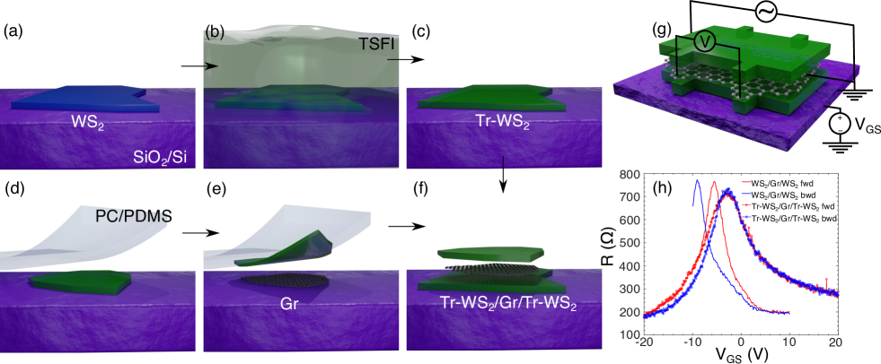
We start our work with fabricating an heterostructure made of Tr-WS2/Gr/Tr-WS2. The fabrication procedure starts with the micro-mechanical cleavage[46] of 6-25 nm-thick WS2 flakes and single layer graphene on 285 nm SiO2+Si chips. Optical microscopy[47] and Raman spectroscopy[31] were used to select the required flakes before proceeding with further processing, as depicted in Fig.1. Next, we prepared the acid solution by dissolving TFSI in 1,2-dichlorethane (DCE) at a concentration of 5 mg/ml. The exfoliated WS2 flakes on SiO2/Si substrates were immersed in the acid for about 30 minutes and then blow dried using a nitrogen gun as shown in Fig.1(a-c). All these processes were performed inside a nitrogen glovebox as suggested by Ref.45. In parallel, we prepared a polycarbonate (PC) stamp and placed it over a polydimethylsiloxane (PDMS) support on a glass slide, in order to be able to dry-transfer the exfoliated flakes, as reported by Ref.23. We then started assembling the heterostructure, by first picking up a Tr-WS2 flake from a SiO2/Si substrate at 40°C, as shown in Fig.1(d). Next, a single layer graphene is picked up using the stamp+Tr-WS2, again at 40°C. Finally, the whole stack is dropped on the bottom Tr-WS2 (Fig.1(c)), followed by release of the PC film at 120°C 1(e-f) and dissolution of PC in chloroform lasting 10 minutes. The above heterostructure is then shaped in the form of an Hall bar (see MethodsIII). In order to disentangle the role of the top and bottom WS2 layers in the device hysteresis, we also prepared an Hall bar where the WS2 layers were not treated with TFSI (WS2/Gr/WS2, untreated heterostucture).
Fig.1(g) is a schematic of our four probe measurement setup: a bias current is driven between the source and drain external contacts, whilst the voltage difference is read between the two inner probes. A back gate voltage is applied through the bottom (Tr-WS2 or WS2)+SiO2 insulating layers. Fig.1(h) shows the four probe resistance measurements performed on the treated and untreated heterostructures by sweeping the back gate voltage (V). In order to evaluate the hysteresis, we performed forward (red) and reverse (blue) sweeps of the untreated (solid line) and treated (line with circles) heterostructures. The untreated heterostructure exhibits a considerable shift in the CNP, V, of 5V). This shift could be explained as follows: when we sweep the back gate voltage, depending on the polarity, electrons or holes transfer from the graphene to trap sites on the substrate and become trapped. On sweeping back the gate voltage, the trapped charges electrostatically dope graphene, which manifests in shifting its CNP[38]. In our heterostructure, hysteresis is caused by the charge trapping of carriers from graphene within the WS2 vacancy sites[48, 49] and also at the interface with the SiO2 surface[38], with the former being orders of magnitude more dominant with respect to the latter[42, 50, 38]. The heterostructure sample shows less than an order of magnitude hysteresis compared with the untreated heterostructure, with a V of 0.2V. The charge trap density is then also a measure of the sample hysteresis and can be calculated from the V as[38]:
| (1) |
where Cg is the gate capacitance calculated from:
| (2) |
As we gate graphene through two dielectrics, here is the relative permittivity of SiO2 (3.9), is the relative permittivity of WS2 (6.2, from Ref.51), is the vacuum permittivity, while and are the thickness values of SiO2 and WS2, respectively. We measured a trap density of cm-2 for the untreated heterostructure and cm-2 for the Tr-WS2/Gr/Tr-WS2 (treated heterostructure) by taking the absolute difference between the maximum values in resistance in forward and backward sweeps. However, we note that the resistance of the sample fluctuates, potentially masking the correct position of the CNP. A difference of 0.7 V (corresponding to cm-2) is indeed observed between the position of the CNP taken from the raw data as the maximum value of resistance and the same value taken while smoothing the data, instead. We then infer that a more conservative value of cm-2 can be claimed as upper bound of hysteresis, which is certainly not overcome by the treated heterostructure. From now on we refer to this value as the noise level. This clearly indicates that the TFSI treatment played a crucial role in suppressing the defect sites, drastically decreasing the device hysteresis by almost one order of magnitude compared to the untreated WS2/Gr/WS2 heterostructure.
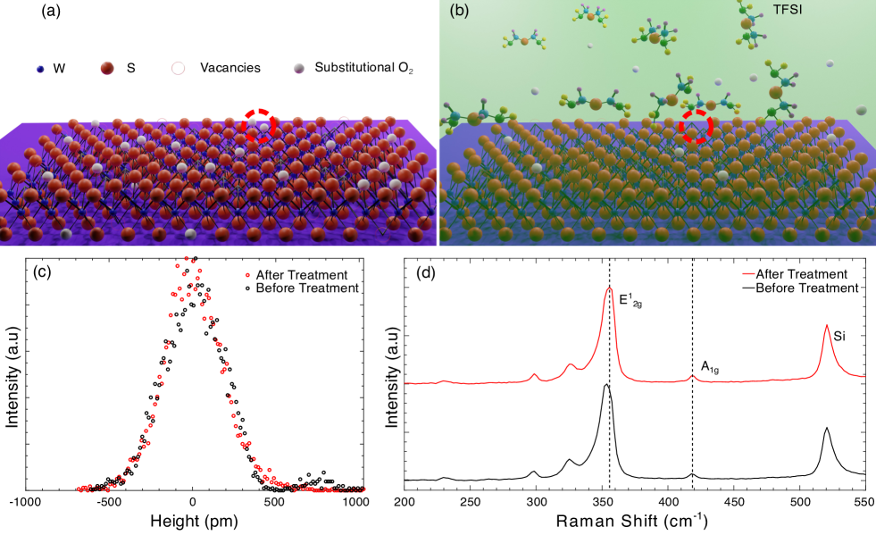
In order to be able to address the exhibited behaviour of the treated heterostructure in Fig.1(h) one has to carefully analyse the existing problem of hysteresis in TMD-based devices and the origin of such effect. The predominant intrinsic defect types in as-exfoliated and as-grown TMDs are chalcogen vacancies, depicted as hollow spheres in Fig.2[52]. At ambient conditions, these vacancies are often filled with substitutional atoms, mainly oxygen[53, 54, 55], represented as white spheres in Fig.2. Depending on their concentration, defects can considerably alter the electronic and optical properties of TMD-based devices[56, 57]. Vacancies represent the main source of trapping/detrapping of charges[48], which in turn results in hysteresis effects[36, 37], especially when a TMD is used as a dielectric. Many methods have been proposed to eliminate the substitutional atoms and/or “passivate” the vacancies with the original chalcogen atom species[43, 44, 45, 58].
In this work, we chose to perform a non invasive chemical approach as proposed in Ref.43. As schematized by the red dashed circle in Fig.2(a) and (b), the treatment with TFSI removes the substitutional oxygen atoms or any other absorbed contaminant and passivates the vacancy site[43, 45]. Performing a chemical treatment could theoretically deteriorate the morphological properties of the TMD. For this reason we scanned by atomic force microscopy (AFM) an area of 15 m15 m of the sample before and after the treatment (2(c) and insets) and we plotted an histogram of the height profiles. Black and red circles represent height profiles of the samples acquired before and after the chemical treatment, respectively. On fitting these height distributions with a Gaussian, we obtain a standard deviation which points towards a roughness around 155 pm and 145 pm for the sample before and after the treatment, respectively. These AFM results suggest that the chemical treatment had produced no significant morphological change to the material surface. Raman characterisation was also performed using a Renishaw Invia Spectrometer with 532 nm laser excitation and a 100 objective lens. Raman spectra of the WS2 flake on SiO2/Si before and after treatment are represented as the black and red lines in Fig.2(d), respectively. On carefully examining the E mode at 350 cm-1 and the A mode at 420 cm-1, we observe a slight blue-shift after the treatment, which has been associated with a reduction of the doping in the sample[58, 60, 61]. This effect is in agreement with the removal of the substitutional oxygen and passivation of the vacancy sites by the TFSI treatment explained earlier. Results from AFM and Raman demonstrate the robustness of the TFSI treatment, and therefore open a path for the exploration of more complicated heterostructures.
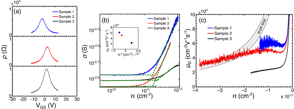
We then fabricated three different Hall bars out of Tr-WS2/Gr/Tr-WS2 heterostructures (which we name here as Sample 1, 2, 3, respectively), with thickness of the top and bottom WS2 layers in the range 6-25 nm. The length and width of the Hall bars are =2 m-=7 m for Sample 1, =4 m-=10 m for Sample 2, and =1.5 m-=2.5 m for Sample 3. We focused on the transport properties of such Hall bars measured at room temperature. Fig.3(a) is the resistivity () of the treated Samples 1-3 measured while sweeping the backgate voltage V. Here we use resistivity instead of resistance to have a more direct comparison among the three samples without accounting for geometrical differences among the Hall bars. The CNP in the three samples is positioned within ± 2.7 V from zero gate bias, which correspond to variations in the Fermi level of graphene (at zero gate bias) in the three samples within ± 74 meV[59], indicating a minimal doping. The values in Samples 1-3 are comparable, varying from 640-990 at CNP to 100-120 at high doping. Fig.3(b) shows the measured conductivity of graphene at room temperature, plotted on a double log scale as a function of . The carrier density is calculated from = (VV)/[23]. can be extracted from this plot by noting the intersection point between the two quasi-linear sections of the conductivity plot as highlighted by the green dashed line. The for Sample 1, 2, and 3 are 1.7, 1.8 and 2.2 cm-2, respectively. The Drude mobility is calculated from = /(), where = 1/ is the conductivity of graphene. At technologically relevant charge carrier densities 1012 cm-2, Sample 1, 2 and 3, exhibit a of 6.2, 5.0 and 2.5104 cm-2V-1s-1, respectively, as shown in the inset of Fig.3(b). The slight difference in the mobility among the samples, can be correlated to the and agrees well with the inversely linear relationship between and [13].
In general, at higher ( cm-2) carriers couple to acoustic phonons and the mobility degrades[62, 63, 12]. Fig.3(c) is the plot of the as a function of the charge carrier density . The gray shaded region with the black dotted borders illustrates the upper and lower limit of the electron-phonon limited mobility model from Ref.12, which are calculated assuming deformation potential (D) values of 18-20 eV[12]. We then decided to probe the sample with intermediate values of mobility up to a -3.8 cm-2 and we recorded a factor 30% drop in mobility compared to the maximum acceptable value measured at -1 cm-2. This is a factor two lower compared to the mobility drop recorded in hBN-encapsulated graphene devices, which typically undergo a 70% drop in mobility in the same doping range[24, 6]. This behaviour is one crucial advantage of TMD-encapsulated graphene devices over hBN-encapsulated graphene devices, especially in the context of applications such as photodetectors or modulators operating at high doping. A comparison between the record-high mobility obtained with hBN-encapsulated graphene samples and the treated-TMD-encapsulated graphene samples used here would not be fair, as the reported values of the former refer to using hBN thick flakes of 80 nm [23, 24]. In this work the thickness of both top and bottom WS2 layers in all samples were kept below 25 nm. We strived to contain the WS2 thickness below 25 nm so that the used materials would be as similar as possible, in terms of thickness, to those successfully grown in the research community by CVD[33, 34, 35]. While comparing our samples with those using hBN flakes of the same thickness, we obtain similar values of [23].
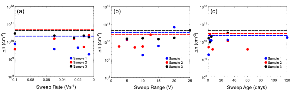
In order to probe the reliability of the treatment and its durability in time, we monitored the in Samples 1-3 while changing the sweep rate, range and re-testing the samples over time. The voltage sweeping rate is very important as reducing the sweep rate gives charges sufficient time to become trapped in the defect site, resulting in higher hysteresis. Therefore, one should expect an increase in hysteresis, while reducing the sweep rate if traps are present in the Tr-WS2. However, Fig.4(a) shows that by reducing the sweep rates from 0.1 Vs-1 to 0.005 Vs-1 no significant change in the hysteresis values occurs: remarkably, all the samples show very low variations of below the noise level for any of the utilised sweep rates, confirming the high efficiency of the treatment in passivating the defect sites and hindering charge trap mechanisms. The of Samples 1-3 are lower than the noise level measured for each of the samples, indicated as color-matched dashed lines in Fig.4(a). Next, we monitored the with respect to the V sweep range, as we should expect an increase in the device hysteresis with the increase in the voltage sweep range[38]. This is due to the fact that, by increasing the V sweep range, more and more carriers become available for transport, but they are also more likely to become trapped in the defect sites. In Fig.4(b) we plot against various gate voltage ranges, where, for example, a V sweep from -10 V to 10 V corresponds to a voltage range of 10 V, considering the CNP being close to 0 V. The measurement range of each sample is limited by the WS2 and SiO2 breakdown voltages, assumed to be 0.1 MVcm-1[64] and 15 MVcm-1[65], respectively. For these measurements the sweep rate is kept constant at 0.0125 Vs-1. Samples show almost no dependence on the sweep range with kept consistently below cm-2. However, when the V sweep range was increased to 20 V for Sample 1, having 6 nm bottom Tr-WS2 thickness, we start to notice an increase in to cm-2. This particular behaviour could be attributed to the onset of the dielectric breakdown of the the bottom Tr-WS2 flake[64].
Next, the of the treated heterostructures is monitored at regular time intervals to check the integrity of the TFSI treatment over time. For these measurements we also adopted a sweep rate of 0.0125 Vs-1. Samples were measured until 120 days from the fabrication date and data are shown in Fig.4(c). All the three samples show again no dependency towards the ageing, confirming the resilience of the chemical treatment. It is worth mentioning that the samples were stored in ambient lab atmosphere for the entire duration of this experiment. In any of the measurement conditions has never overcome cm-2. To highlight the significance of the hysteresis treatment when measuring a Tr-WS2/Gr/Tr-WS2 heterostructure, we outline the noise level of the Samples 1-3 in each of the graphs of Fig.4, and all the data-points are below such values of noise, proving that the hysteresis is indeed minimal.
II Conclusion
In conclusion, we have demonstrated that TFSI-treated WS2 can be an excellent choice for encapsulating graphene and also performs well as gate dielectric. The TFSI treatment is highly stable, resilient and it drastically reduces the hysteresis in high mobility WS2/Gr/WS2 heterostructures. This could be due to the removal and replacement of substitutional atoms responsible for charge traps, as suggested by a Raman analysis and transport measurements. The hysteresis remains well under cm-2, even when the sample is subjected to large sweep rates, range and ageing tests. This hysteresis value is at least five times smaller than that measured in an untreated heterostructure. In one treated heterostructure we achieved a mobility as high as 6.0104 cm-2V-1s-1. Due to the weak influence of surface acoustic phonons, the mobility of the treated heterostructures are almost flat up to cm-2. These results suggest that TMD/Gr/TMD heterostructures could be adopted in advanced optoelectronic applications requiring low hysteresis and high mobility at high carrier concentrations.
III Methods
Materials: WS2 highly crystalline van der Waals (vdW) crystals were synthesized through the self-flux technique. In the first step, the stoichiometric ratio of elemental puratronic grade (99.9999% pure) purity tungsten powder and sublimation purified sulfur powder (99.9999% pure) were mixed and sealed under 10-6 Torr inside a quartz ampoule. The powder was heated at 950°C for 5 days to create vdW powders. In the second step, these pre-reacted powders were resealed in a quartz ampoule with extra sulfur to reach 1:2 stoichiometry. In the second step, all the ingredients were kept at a high-temperature zone (1040°C) with a temperature drop of 50°C to initiate the vapor transport and realize vdW WS2 crystals after 7 weeks. The resultant crystals measured 2-6 mm in size. Overall, the crystal appearance and spectroscopic signatures were superior to chemical vapor transported crystals. Single layer graphene was exfoliated from highly-oriented pyrolytic graphite (HOPG) commercially bought from HQ Graphene labelled as natural graphite. TFSI (product number 15220) and 1,2-dichlorethane (DCE) (product number 284505) were bought from Sigma-Aldrich.
Fabrication: Lithography was performed by using an Inspect F50 RAITH Elphy Plus system and a poly(methyl methacrylate) (PMMA) mask. The heterostructure was then dry-etched (reactive ion etching) using a trifluoromethane/oxygen (CHF3/O2) mixture of gases with a flow rate of 40/4 sccm in a Plasmalab System 100 from Oxford Instruments. Cr was deposited thermally with thickness of 5 nm using a Lesker LAB18 evaporator, while Au was deposited thermally with the same instrument and with a 50 nm thickness. The evaporation was followed by an overnight lift-off in acetone, dipping in isopropanol and nitrogen blow-drying.
Electrical Transport Measurement: transport measurements were performed using a Lakeshore cryogenic probe station at a pressure of mbar with a lock-in amplifier from Stanford Research Systems SR810. A bias of 100 nA was applied between the source and drain electrodes with a lock-in modulation frequency of 373 Hz. The gate voltages were applied using a Keithley 2460 sourcemeter.
IV Acknowledgements
The authors acknowledge Matteo Ceccanti for graphical support and Francisco Bernal Texca for his help towards setting up the fabrication steps inside the glovebox. F.H.L.K. acknowledges financial support from the Government of Catalonia trough the SGR grant and from the Spanish Ministry of Economy and Competitiveness through the “Severo Ochoa” Programme for Centres of Excellence in R&D (CEX2019-000910-S), support by Fundacio Cellex Barcelona, Generalitat de Catalunya, through the CERCA program, and the Mineco Grants Plan Nacional (FIS2016-81044-P) and the Agency for Management of University and Research Grants (AGAUR) 2017 SGR 1656. Furthermore, the research leading to these results has received funding from the European Commission in the Horizon 2020 Framework Programme under Grant Agreements Nos. 785219 (Core2) and 881603 (Core3) of the Graphene Flagship. This work was also financially supported by the German Science Foundation (DFG) within the priority program FFlexCom Project “GLECS” (Contract No. NE1633/3). D.D.F. acknowledges funding from the “Severo Ochoa” Excellence Programme. S.T acknowledges support from DOE-SC0020653 (materials synthesis), NSF DMR-2206987 (magnetic characterization), NSF ECCS 2052527 (electrical optimization), and NSF DMR 2111812 (optical optimization).
References
- [1] S. M. Sze and K. K. Ng, Physics of Semiconductor Devices (John Wiley and Sons, Inc., 2006).
- [2] M. Romagnoli, V. Sorianello, M. Midrio, F. H. L. Koppens, C. Huyghebaert, D. Neumaier, P. Galli, W. Templ, A. D’Errico, and A. C. Ferrari, Graphene-Based Integrated Photonics for next-Generation Datacom and Telecom, Nat. Rev. Mater. 3, 392 (2018).
- [3] Y. Kang, H. D. Liu, M. Morse, M. J. Paniccia, M. Zadka, S. Litski, G. Sarid, A. Pauchard, Y. H. Kuo, H. W. Chen, W. S. Zaoui, J. E. Bowers, A. Beling, D. C. McIntosh, X. Zheng, and J. C. Campbell, Monolithic Germanium/Silicon Avalanche Photodiodes with 340 GHz Gain–Bandwidth Product, Nat. Photonics 3, 59 (2008).
- [4] J. E. Muench, A. Ruocco, M. A. Giambra, V. Miseikis, D. Zhang, J. Wang, H. F. Y. Watson, G. C. Park, S. Akhavan, V. Sorianello, M. Midrio, A. Tomadin, C. Coletti, M. Romagnoli, A. C. Ferrari, and I. Goykhman, Waveguide-Integrated, Plasmonic Enhanced Graphene Photodetectors, Nano Lett. 19, 7632 (2019).
- [5] Z. Wang, L. Banszerus, M. Otto, K. Watanabe, T. Taniguchi, C. Stampfer, and D. Neumaier, Encapsulated Graphene-Based Hall Sensors on Foil with Increased Sensitivity, Phys. Status Solidi 253, 2316 (2016).
- [6] L. Wang, I. Meric, P. Y. Huang, Q. Gao, Y. Gao, H. Tran, T. Taniguchi, K. Watanabe, L. M. Campos, D. A. Muller, J. Guo, P. Kim, J. Hone, K. L. Shepard, and C. R. Dean, One-Dimensional Electrical Contact to a Two-Dimensional Material, Science 342, 614 (2013).
- [7] R. R. Nair, P. Blake, A. N. Grigorenko, K. S. Novoselov, T. J. Booth, T. Stauber, N. M. R. Peres, and A. K. Geim, Fine Structure Constant Defines Visual Transparency of Graphene, Science 320, 1308 (2008).
- [8] S. Bae, H. Kim, Y. Lee, X. Xu, J. S. Park, Y. Zheng, J. Balakrishnan, T. Lei, H. Ri Kim, Y. Il Song, Y. J. Kim, K. S. Kim, B. Özyilmaz, J. H. Ahn, B. H. Hong, and S. Iijima, Roll-to-Roll Production of 30-Inch Graphene Films for Transparent Electrodes, Nat. Nanotechnol. 5, 574 (2010).
- [9] E. S. Polsen, D. Q. McNerny, B. Viswanath, S. W. Pattinson, and A. John Hart, High-Speed Roll-to-Roll Manufacturing of Graphene Using a Concentric Tube CVD Reactor, Sci. Rep. 5, 1 (2015).
- [10] S. Goossens, G. Navickaite, C. Monasterio, S. Gupta, J. J. Piqueras, R. Pérez, G. Burwell, I. Nikitskiy, T. Lasanta, T. Galán, E. Puma, A. Centeno, A. Pesquera, A. Zurutuza, G. Konstantatos, and F. Koppens, Broadband Image Sensor Array Based on Graphene–CMOS Integration, Nat. Photonics 11, 366 (2017).
- [11] D. Akinwande, C. Huyghebaert, C. H. Wang, M. I. Serna, S. Goossens, L. J. Li, H. S. P. Wong, and F. H. L. Koppens, Graphene and Two-Dimensional Materials for Silicon Technology, Nature 573, 507 (2019).
- [12] E. H. Hwang and S. Das Sarma, Acoustic Phonon Scattering Limited Carrier Mobility in Two-Dimensional Extrinsic Graphene, Phys. Rev. B 77, 115449 (2008).
- [13] N. J. G. Couto, D. Costanzo, S. Engels, D. K. Ki, K. Watanabe, T. Taniguchi, C. Stampfer, F. Guinea, and A. F. Morpurgo, Random Strain Fluctuations as Dominant Disorder Source for High-Quality on-Substrate Graphene Devices, Phys. Rev. X 4, 041019 (2014).
- [14] C. Neumann, S. Reichardt, P. Venezuela, M. Drögeler, L. Banszerus, M. Schmitz, K. Watanabe, T. Taniguchi, F. Mauri, B. Beschoten, S. V. Rotkin, and C. Stampfer, Raman Spectroscopy as Probe of Nanometre-Scale Strain Variations in Graphene, Nat. Commun. 6, 1 (2015).
- [15] C. R. Dean, A. F. Young, I. Meric, C. Lee, L. Wang, S. Sorgenfrei, K. Watanabe, T. Taniguchi, P. Kim, K. L. Shepard, and J. Hone, Boron Nitride Substrates for High-Quality Graphene Electronics, Nat. Nanotechnol. 5, 722 (2010).
- [16] K. I. Bolotin, K. J. Sikes, Z. Jiang, M. Klima, G. Fudenberg, J. Hone, P. Kim, and H. L. Stormer, Ultrahigh Electron Mobility in Suspended Graphene, Solid State Commun. 146, 351 (2008).
- [17] M. A. Giambra, V. Mišeikis, S. Pezzini, S. Marconi, A. Montanaro, F. Fabbri, V. Sorianello, A. C. Ferrari, C. Coletti, and M. Romagnoli, Wafer-Scale Integration of Graphene-Based Photonic Devices, ACS Nano 15, 3171 (2021).
- [18] S. Kim, J. Nah, I. Jo, D. Shahrjerdi, L. Colombo, Z. Yao, E. Tutuc, and S. K. Banerjee, Realization of a High Mobility Dual-Gated Graphene Field-Effect Transistor with Al2O3 Dielectric, Appl. Phys. Lett. 94, 062107 (2009).
- [19] J. Gun Oh, S. Ki Hong, C. K. Kim, J. Hoon Bong, J. Shin, S. Y. Choi, and B. Jin Cho, High Performance Graphene Field Effect Transistors on an Aluminum Nitride Substrate with High Surface Phonon Energy, Appl. Phys. Lett. 104, 193112 (2014).
- [20] M. E. Ramón, K. N. Parrish, S. F. Chowdhury, C. W. Magnuson, H. C. P. Movva, R. S. Ruoff, S. K. Banerjee and D. Akinwande, IEEE Trans. Nanotechnol 11, 877 (2012).
- [21] N. J. G. Couto, B. Sacépé, and A. F. Morpurgo, Transport through Graphene on SrTiO3, Phys. Rev. Lett. 107, 225501 (2011).
- [22] P. Klar, E. Lidorikis, A. Eckmann, I. A. Verzhbitskiy, A. C. Ferrari, and C. Casiraghi, Raman Scattering Efficiency of Graphene, Phys. Rev. B 87, 205435 (2013).
- [23] D. G. Purdie, N. M. Pugno, T. Taniguchi, K. Watanabe, A. C. Ferrari, and A. Lombardo, Cleaning Interfaces in Layered Materials Heterostructures, Nat. Commun. 9, 1 (2018).
- [24] Z. Huang, A. Alharbi, W. Mayer, E. Cuniberto, T. Taniguchi, K. Watanabe, J. Shabani, and D. Shahrjerdi, Versatile Construction of van Der Waals Heterostructures Using a Dual-Function Polymeric Film, Nat. Commun. 11, 1 (2020).
- [25] S. Pezzini, V. Mišeikis, S. Pace, F. Rossella, K. Watanabe, T. Taniguchi, and C. Coletti, High-Quality Electrical Transport Using Scalable CVD Graphene, 2D Mater. 7, 041003 (2020).
- [26] S. M. Kim, A. Hsu, M. H. Park, S. H. Chae, S. J. Yun, J. S. Lee, D. H. Cho, W. Fang, C. Lee, T. Palacios, M. Dresselhaus, K. K. Kim, Y. H. Lee, and J. Kong, Synthesis of Large-Area Multilayer Hexagonal Boron Nitride for High Material Performance, Nat. Commun. 6, 1 (2015).
- [27] Y. Shen, W. Zheng, K. Zhu, Y. Xiao, C. Wen, Y. Liu, X. Jing, M. Lanza, Y. Shen, W. Zheng, Y. Xiao, C. Wen, Y. Liu, X. Jing, K. Zhu, and M. Lanza, Variability and Yield in H-BN-Based Memristive Circuits: The Role of Each Type of Defect, Adv. Mater. 33, 2103656 (2021).
- [28] V. Shautsova, A. M. Gilbertson, N. C. G. Black, S. A. Maier, and L. F. Cohen, Hexagonal Boron Nitride Assisted Transfer and Encapsulation of Large Area CVD Graphene, Sci. Rep. 6, 1 (2016).
- [29] L. Banszerus, T. Sohier, A. Epping, F. Winkler, F. Libisch, F. Haupt, K. Watanabe, T. Taniguchi, K. Müller-Caspary, N. Marzari, F. Mauri, B. Beschoten, and C. Stampfer, Extraordinary High Room-Temperature Carrier Mobility in Graphene-WSe2 Heterostructures, arXiv:1909.09523 (2019).
- [30] L. Banszerus, H. Janssen, M. Otto, A. Epping, T. Taniguchi, K. Watanabe, B. Beschoten, D. Neumaier, and C. Stampfer, Identifying Suitable Substrates for High-Quality Graphene-Based Heterostructures, 2D Mater. 4, 025030 (2017).
- [31] A. C. Ferrari, J. C. Meyer, V. Scardaci, C. Casiraghi, M. Lazzeri, F. Mauri, S. Piscanec, D. Jiang, K. S. Novoselov, S. Roth, and A. K. Geim, Raman Spectrum of Graphene and Graphene Layers, Phys. Rev. Lett. 97, 187401 (2006).
- [32] A. C. Ferrari and D. M. Basko, Raman Spectroscopy as a Versatile Tool for Studying the Properties of Graphene, Nat. Nanotechnol. 8, 235 (2013).
- [33] C. Jung, S. M. Kim, H. Moon, G. Han, J. Kwon, Y. K. Hong, I. Omkaram, Y. Yoon, S. Kim, and J. Park, Highly Crystalline CVD-Grown Multilayer MoSe2 Thin Film Transistor for Fast Photodetector, Sci. Rep. 5, 1 (2015).
- [34] P. D. Cunningham, K. M. McCreary, A. T. Hanbicki, M. Currie, B. T. Jonker, and L. M. Hayden, Charge Trapping and Exciton Dynamics in Large-Area CVD Grown MoS2, J. Phys. Chem. C 120, 5819 (2016).
- [35] T. Schram, Q. Smets, B. Groven, M. H. Heyne, E. Kunnen, A. Thiam, K. Devriendt, A. Delabie, D. Lin, M. Lux, D. Chiappe, I. Asselberghs, S. Brus, C. Huyghebaert, S. Sayan, A. Juncker, M. Caymax, and I. P. Radu, WS2 Transistors on 300 Mm Wafers with BEOL Compatibility, Eur. Solid-State Device Res. Conf. 212 (2017).
- [36] H. Wang, D. Ren, C. Lu, and X. Yan, Investigation of Multilayer WS2 Flakes as Charge Trapping Stack Layers in Non-Volatile Memories, Appl. Phys. Lett. 112, 231903 (2018).
- [37] H. An, Y. H. Lee, J. H. Lee, C. Wu, B. M. Koo, and T. W. Kim, Highly Stable and Flexible Memristive Devices Based on Polyvinylpyrrolidone: WS2 Quantum Dots, Sci. Rep. 10, 1 (2020).
- [38] H. Wang, Y. Wu, C. Cong, J. Shang, and T. Yu, Hysteresis of Electronic Transport in Graphene Transistors, ACS Nano 4, 7221 (2010).
- [39] K. S. Novoselov, A. K. Geim, S. V. Morozov, D. Jiang, Y. Zhang, S. V. Dubonos, I. V. Grigorieva, and A. A. Firsov, Electric Field in Atomically Thin Carbon Films, Science 306, 666 (2004).
- [40] J. Roh, J. H. Lee, S. H. Jin, and C. Lee, Negligible Hysteresis of Molybdenum Disulfide Field-Effect Transistors through Thermal Annealing, J. Inf. Disp. 17, 103 (2016).
- [41] C. Lan, X. Kang, Y. Meng, R. Wei, X. Bu, S. Yip, and J. C. Ho, The Origin of Gate Bias Stress Instability and Hysteresis in Monolayer WS2 Transistors, Nano Res. 13, 3278 (2020).
- [42] H. Qiu, T. Xu, Z. Wang, W. Ren, H. Nan, Z. Ni, Q. Chen, S. Yuan, F. Miao, F. Song, G. Long, Y. Shi, L. Sun, J. Wang, and X. Wang, Hopping Transport through Defect-Induced Localized States in Molybdenum Disulphide, Nat. Commun. 4, 1 (2013).
- [43] M. Amani, D. H. Lien, D. Kiriya, J. Xiao, A. Azcatl, J. Noh, S. R. Madhvapathy, R. Addou, K. C. Santosh, M. Dubey, K. Cho, R. M. Wallace, S. C. Lee, J. H. He, J. W. Ager, X. Zhang, E. Yablonovitch, and A. Javey, Near-Unity Photoluminescence Quantum Yield in MoS2, Science 350, 1065 (2015).
- [44] H. Kim, D. H. Lien, M. Amani, J. W. Ager, and A. Javey, Highly Stable Near-Unity Photoluminescence Yield in Monolayer MoS2 by Fluoropolymer Encapsulation and Superacid Treatment, ACS Nano 11, 5179 (2017).
- [45] H. Bretscher, Z. Li, J. Xiao, D. Y. Qiu, S. Refaely-Abramson, J. A. Alexander-Webber, A. Tanoh, Y. Fan, G. Delport, C. A. Williams, S. D. Stranks, S. Hofmann, J. B. Neaton, S. G. Louie, and A. Rao, Rational Passivation of Sulfur Vacancy Defects in Two-Dimensional Transition Metal Dichalcogenides, ACS Nano 15, 8780 (2021).
- [46] K. S. Novoselov, D. Jiang, F. Schedin, T. J. Booth, V. V. Khotkevich, S. V. Morozov, and A. K. Geim, Two-Dimensional Atomic Crystals, Proc. Natl. Acad. Sci. 102, 10451 (2005).
- [47] C. Casiraghi, A. Hartschuh, E. Lidorikis, H. Qian, H. Harutyunyan, T. Gokus, K. S. Novoselov, and A. C. Ferrari, Rayleigh Imaging of Graphene and Graphene Layers, Nano Lett. 7, 2711 (2007).
- [48] H. Nan, Z. Wang, W. Wang, Z. Liang, Y. Lu, Q. Chen, D. He, P. Tan, F. Miao, X. Wang, J. Wang, and Z. Ni, Strong Photoluminescence Enhancement of MoS2 through Defect Engineering and Oxygen Bonding, ACS Nano 8, 5738 (2014).
- [49] L. Li and E. A. Carter, Defect-Mediated Charge-Carrier Trapping and Nonradiative Recombination in WSe2 Monolayers, J. Am. Chem. Soc. 141, 10451 (2019).
- [50] T. Ando, A. B. Fowler, and F. Stern, Electronic Properties of Two-Dimensional Systems, Rev. Mod. Phys. 54, 437 (1982).
- [51] A. Laturia, M. L. Van de Put, and W. G. Vandenberghe, Dielectric Properties of Hexagonal Boron Nitride and Transition Metal Dichalcogenides: From Monolayer to Bulk, Npj 2D Mater. Appl. 2, 1 (2018).
- [52] Z. Lin, B. R. Carvalho, E. Kahn, R. Lv, R. Rao, H. Terrones, M. A. Pimenta, and M. Terrones, Defect Engineering of Two-Dimensional Transition Metal Dichalcogenides, 2D Mater. 3, 022002 (2016).
- [53] Y. Liu, P. Stradins, S.-H. Wei, Y. Liu, P. Stradins, and S.-H. Wei, Air Passivation of Chalcogen Vacancies in Two-Dimensional Semiconductors, Angew. Chemie Int. Ed. 55, 965 (2016).
- [54] J. Pető, T. Ollár, P. Vancsó, Z. I. Popov, G. Z. Magda, G. Dobrik, C. Hwang, P. B. Sorokin, and L. Tapasztó, Spontaneous Doping of the Basal Plane of MoS2 Single Layers through Oxygen Substitution under Ambient Conditions, Nat. Chem. 10, 1246 (2018).
- [55] S. Barja, S. Refaely-Abramson, B. Schuler, D. Y. Qiu, A. Pulkin, S. Wickenburg, H. Ryu, M. M. Ugeda, C. Kastl, C. Chen, C. Hwang, A. Schwartzberg, S. Aloni, S. K. Mo, D. Frank Ogletree, M. F. Crommie, O. V. Yazyev, S. G. Louie, J. B. Neaton, and A. Weber-Bargioni, Identifying Substitutional Oxygen as a Prolific Point Defect in Monolayer Transition Metal Dichalcogenides, Nat. Commun. 10, 1 (2019).
- [56] W. Wang, L. Bai, C. Yang, K. Fan, Y. Xie, and M. Li, The Electronic Properties of O-Doped Pure and Sulfur Vacancy-Defect Monolayer WS2: A First-Principles Study, Mater. 11, 218 (2018).
- [57] Z. He, X. Wang, W. Xu, Y. Zhou, Y. Sheng, Y. Rong, J. M. Smith, and J. H. Warner, Revealing Defect-State Photoluminescence in Monolayer WS2 by Cryogenic Laser Processing, ACS Nano 10, 5847 (2016).
- [58] Y. Liu, H. Liu, J. Wang, and D. Liu, Defect-Type-Dependent Carrier Lifetimes in Monolayer WS2 Films, J. Phys. Chem. C 126, 4929 (2022).
- [59] A. Das, S. Pisana, B. Chakraborty, S. Piscanec, S. K. Saha, U. V. Waghmare, K. S. Novoselov, H. R. Krishnamurthy, A. K. Geim, A. C. Ferrari, and A. K. Sood, Monitoring Dopants by Raman Scattering in an Electrochemically Top-Gated Graphene Transistor, Nat. Nanotechnol. 3, 210 (2008).
- [60] J. Yang, J. U. Lee, and H. Cheong, Excitation Energy Dependence of Raman Spectra of Few-Layer WS2, FlatChem 3, 64 (2017).
- [61] W. Zhao, Z. Ghorannevis, K. K. Amara, J. R. Pang, M. Toh, X. Zhang, C. Kloc, P. H. Tan, and G. Eda, Lattice Dynamics in Mono- and Few-Layer Sheets of WS2 and WSe2, Nanoscale 5, 9677 (2013).
- [62] A. Principi, M. Carrega, M. B. Lundeberg, A. Woessner, F. H. L. Koppens, G. Vignale, and M. Polini, Plasmon Losses Due to Electron-Phonon Scattering: The Case of Graphene Encapsulated in Hexagonal Boron Nitride, Phys. Rev. B 90, 165408 (2014).
- [63] M. A. Yamoah, W. Yang, E. Pop, and D. Goldhaber-Gordon, High-Velocity Saturation in Graphene Encapsulated by Hexagonal Boron Nitride, ACS Nano 11, 9914 (2017).
- [64] Y. Fan, A. W. Robertson, Y. Zhou, Q. Chen, X. Zhang, N. D. Browning, H. Zheng, M. H. Rümmeli, and J. H. Warner, Electrical Breakdown of Suspended Mono- and Few-Layer Tungsten Disulfide via Sulfur Depletion Identified by in Situ Atomic Imaging, ACS Nano 11, 9435 (2017).
- [65] J. W. McPherson, J. Kim, A. Shanware, H. Mogul, and J. Rodriguez, Trends in the Ultimate Breakdown Strength of High Dielectric-Constant Materials, IEEE Trans. Electron Devices 50, 1771 (2003).