Charge carriers trapping by the full-configuration defects in metal halide perovskites quantum dots
Abstract
Metal halide perovskites quantum dots (MHPQDs) have aroused enormous interesting in the photovoltaic and photoelectric because of their marvelous properties and size characteristics. However, one of key problems that how to systematically analyze charge carriers trapping by different defects is still a challenge task. Here, we study nonradiation multiphonon processes of the charge carrier trapping by various defects in MHPQDs based on the well-known Huang-Rhys model, in which a method of full-configuration defect, including different defect species with variable depth and lattice relaxation strength, is developed by introducing a localization parameter in the quantum defect model. With the help of this method, these fastest trapping channels for charge carriers transferring from the quantum dot ground state to different defects are found. Furthermore, the dependences of the trapping time on the radius of quantum dot, the defect depth and temperature are given. These results not only enrich the knowledge of charge carrier trapping processes by defects, but enlighten the designs of MHPQDs-based photovoltaic and photoelectric devices.
keywords:
American Chemical Society, LaTeXTianjin University] Tianjin Key Laboratory of Low Dimensional Materials Physics and Preparing Technology, Department of Physics, School of Science, Tianjin University, Tianjin 300354, China Tianjin University] Tianjin Key Laboratory of Low Dimensional Materials Physics and Preparing Technology, Department of Physics, School of Science, Tianjin University, Tianjin 300354, China Tianjin University] Tianjin Key Laboratory of Low Dimensional Materials Physics and Preparing Technology, Department of Physics, School of Science, Tianjin University, Tianjin 300354, China Tianjin University] Tianjin Key Laboratory of Low Dimensional Materials Physics and Preparing Technology, Department of Physics, School of Science, Tianjin University, Tianjin 300354, China Tianjin University] Tianjin Key Laboratory of Low Dimensional Materials Physics and Preparing Technology, Department of Physics, School of Science, Tianjin University, Tianjin 300354, China Tianjin University] Tianjin Key Laboratory of Low Dimensional Materials Physics and Preparing Technology, Department of Physics, School of Science, Tianjin University, Tianjin 300354, China Tianjin University] Tianjin Key Laboratory of Low Dimensional Materials Physics and Preparing Technology, Department of Physics, School of Science, Tianjin University, Tianjin 300354, China Tianjin University] Tianjin Key Laboratory of Low Dimensional Materials Physics and Preparing Technology, Department of Physics, School of Science, Tianjin University, Tianjin 300354, China Tianjin University] Tianjin Key Laboratory of Low Dimensional Materials Physics and Preparing Technology, Department of Physics, School of Science, Tianjin University, Tianjin 300354, China \abbreviationsIR,NMR,UV
TOC Graphic
1 Introduction
Metal halide perovskites quantum dots (MHPQDs) have gained extensive attention in the past few years due to their excellent photoelectric properties such as tunable bandgap, long carrier diffusion length, narrow emission width, high photoluminescence quantum yield and high defect tolerance.1, 2, 3, 4 The power conversion efficiency of MHPQDs-based solar cell has remarkably increased to 16.6% in a relatively short period of time.4 Besides in photovoltaic field, MHPQDs also exhibit immense potential applications in light-emitting diodes and lasers.5, 6, 7 MHPQDs have the size-tunability of their bandgap energies due to quantum confinement effect,8, 9 which enriches the wavelength range of absorption and emission.10, 6 At the same time, the enhancement of quantum confinement effect and the weakening of dielectric screening effect can result in the larger exciton binding energy and enhance the photoluminescent efficiency.11, 12, 6 These structural features are apparently conducive to MHPQDs’ applications. It is just the zero-dimensional structure with specific surface area, giving inevitably rise to various defects in fabrication processes.4 These defects, especially the deep level defects, mediated as the non-radiative recombination centers (or called as the trapping centers),13, 14, 15 leading to charge and energy losses.
There were many experimental strategies have been made to reduce or modify the pernicious influence of defects on material properties.16, 17, 18, 19 Undoubtedly, a series of new experimental method for this issue will be sprang up rapidly in following years. In the theoretical aspect, the dynamical processes of different types of defects in MHPQDs have been extensively studied by first-principal calculation based on the density function theory.20, 21 However, on the one hand, there are still numbers of pernicious defects in MHPQD due to its soft lattice structure,22, 23 resulting in the comprehensively analysis of these defects become almost impossible, even though costing the huge calculational labor. On the other hand, the simulation for the trapping probability (or trapping time) of the charge carrier by so many defects is also a challenge task based on first-principal calculation. In particular, the disagreement between the experimental measurement and the theoretical simulation becomes obviously with the increasing of quantum dots size and temperature. Therefore, an effective method not only classifying so many defects clearly, but also covering all possible trapping channels of the charge carrier by defects is needed urgently.
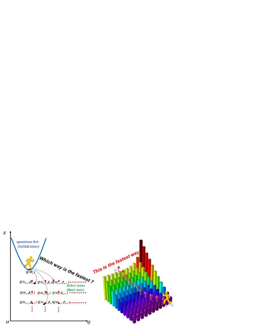
In this paper, we propose a full-configuration defect model by introducing a localization parameter in the classical quantum defect model,24, 25, 26 which allows us not only to classify various defects into three types (accepter-like and donor-like and neutral defects),27 but also to effectively describe the variational defect depth in bandgap with the appropriate lattice relaxation strength. By virtue of this model, we present charge carriers are trapped from the ground state (GS) of MHPQDs to different defect states by non-radiation multiphonon processes, in which the fastest trapping channel is found. More important is that the relations of the fastest channel with the radius of quantum dot, the defect depth and temperature could be obtained, which give the direct guideline to analyze the influence of the charge carrier trapping by defects on the performance of the newly devices, such as the open-circuit voltage of MHPQDs solar cells,28, 29, 30 the instability of bias voltage in MHP transistors31, 32 and so on.
2 Results and discussion
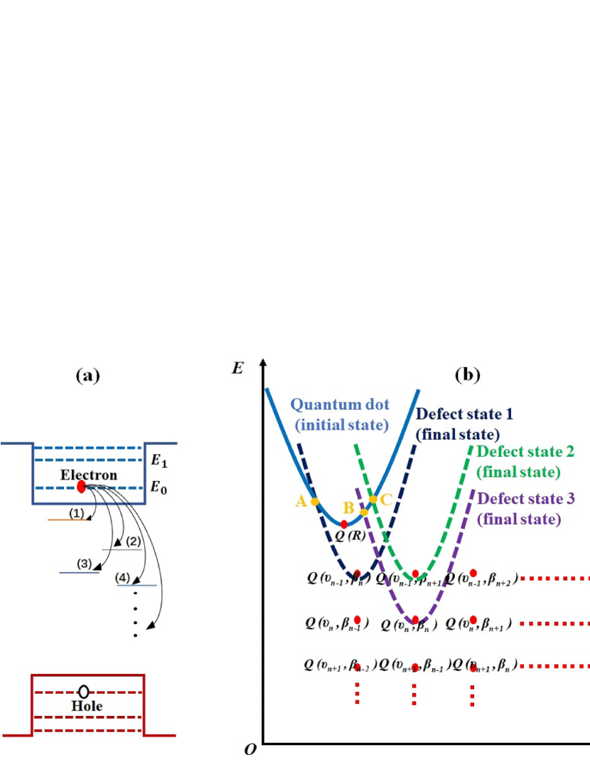
We mainly consider an electron in the ground state in MHP quantum dot are trapped by different depth defects (the trapping process of a hole is similar as electron) as shown in FIG. 1 (a). The eigenwave function and eigenenergy for the quantum dot are given in part A of Supplemental Material. In the classical quantum defect model,24, 25, 26 various defects are divided into three types of donor-like, accepter-like and natural defects by the parameter in the defect wave function, respectively.27 Meanwhile, the variation of defect depth and the corresponding lattice relaxation strength that arising from defects couple with the surrounding lattice filed (or phonon) can be effectively described by the parameter , which is an advantage of this model. However, for the various defects in the same depth with the different lattice relaxation strength are failed description. Therefore, we introduce a localization parameter in the defect wave function to quantitatively describe the lattice relaxation effect for various defects in the same energy level (see the part B of Supplemental Material). Namely, all kinds of defects with varying lattice relaxation strength (thereafter called as full-configuration defects) in these MHP quantum dots could be described by this modified quantum defect model, whose practicability for analyzing the charge carrier trapping will be given further in the following sections.
In the frame of Huang-Rhys model,33, 34, 35, 36 an electron (or a hole) trapping by the defects via non-radiation multiphonon processes are extensively described by the coordinate configuration diagrams shown in FIG. 1 (b), in which the vibrational equilibrium position of system is assumed at when the electron is in the GS state (the initial state), depending on the radius of the quantum dot (), and the equilibrium position shifts to as the electron trapped by defect (the final state), depending on the depth of defect and the localization parameter. The difference between two equilibrium positions can be expressed as:
| (1) | |||||
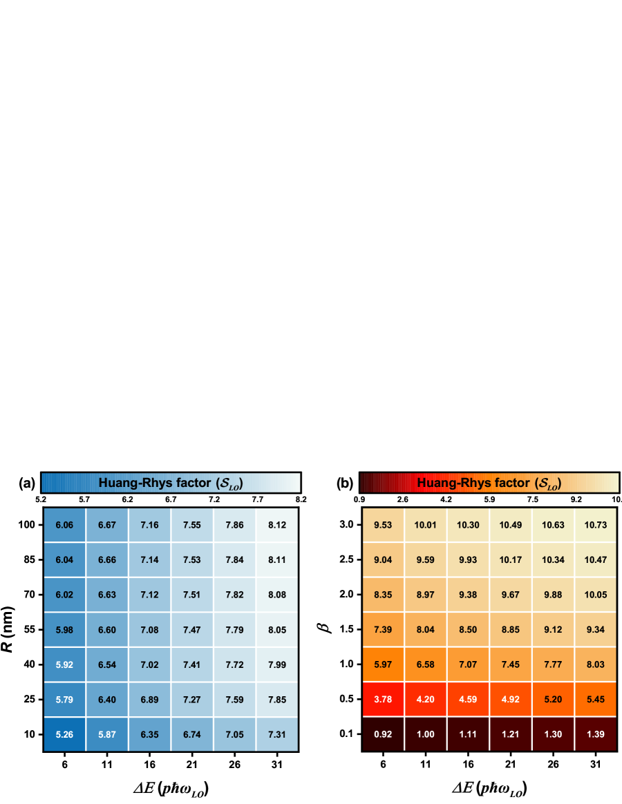
where is the well-known Huang-Rhys factor, in which the longitudinal optical (LO) phonon () and electron-LO phonon coupling () in the Frhlich mechanism are mainly considered, since this coupling plays the dominate rule in the carrier scattering proved by many experiments.23, 37, 38, 39, 40 The detailed expression and calculation for Huang-Rhys factors are present in part C of Supplemental Material. as functions of the depth of donor-like defect and the radius of CH3NH3PbI3 quantum dot are shown in FIG. 2 (a) (the related parameters for CH3NH3PbI3 material are listed in Table 1 in Supplemental Material). One can see that (1) increases obviously with increasing the defect depth, which is consistent with the results of the classical quantum defect model as the variational defects () schemed in FIG. 1 (b);26, 41 (2) increases slightly as the radius increases,42 which can be attributed to the quantum confinement effect become weak with increasing the radius,4, 43, 7 resulting in the difference of equilibrium positions in coordinate configuration between quantum dot and defect are enhanced. The influence of the localization parameter () on are plotted in FIG. 2 (b). From it, one can see that increases signally as varies in the range of 0.13.0 at fixed defect depth. Which reflects the difference strength of lattice relaxation for diverse defects in the same depth in the bandgap as the varying position () schemed in FIG. 1 (b). The similar results for the acceptor-like and neutral defects are also given in FIG. 1 and 2 in Supplemental Material.
In fact, this factor presents an appropriate metric for the systematically energy variation before and after the carrier trapping by different defects. With the aid of this key factor, the trapping probability ( denotes the carrier lifetime or the trapping time) of carrier by various defects via non-radiation multiphonon processes can be written as
| (2) |
where is the transition matrix between GS of quantum dot and defect, whose definition and the related parameters in Eq. (2) are given in part D of Supplemental Material. FIG. 2 (c) shows the carrier lifetime as a function of the defect depth at different radii. One can see that is prolonged by three orders of magnitude as increases, which stems from more LO phonons are required to match the increasing of , hindering the probability of occurrence for the carrier trapping by non-radiation multiphonon processes significantly. Meanwhile, also has the very large changing magnitude with the quantum dot radius, even though varies slightly with the radius shown in FIG. 2 (a), which attributes to the strong effect of quantum confinement of the quantum dot radius on the transition matrix . This implies that the smaller quantum dot, the easier carrier trapping, which is very agreement with the experimental measurements.44, 45, 46 These conclusions are also same as the accepter-like and neutral defects as shown in FIG. 3 and 4 in Supplemental Materials.
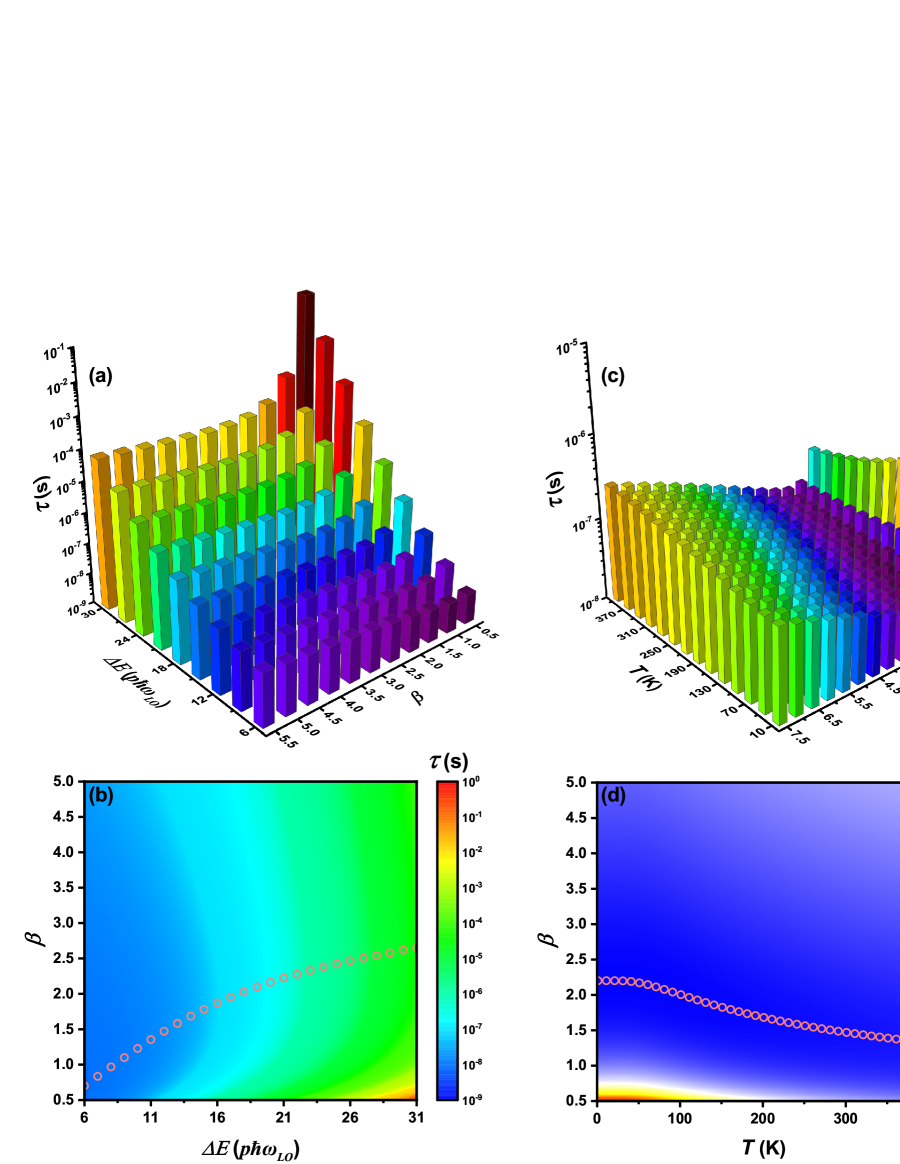
In addition to the defect depth, the localization parameter should play a key role to determine the carrier trapping processes, because which describes the different relaxation strength of the same depth defect with different origins, resulting in the variation of intersection points in the coordinate configurations for before and after the carrier trapping shown in FIG. 1 (b). The influence of and on the are shown in FIG. 3 (a) and (b). We can see that all possible lifetime (or all possible channels) of the carrier trapping by the full-configuration defects can be obtained effectively, whose values are very closely to the results of both first-principle calculation and experimental measurements.47, 48, 49, 50 More important is that the fastest channel (the shortest time) of the carrier trapping can be given as these hollow circles shown in FIG. 3 (b). With the increasing of the defect depth, the charge carriers are inclined to trap by these defects with large localization parameter , which a complement for the only case of in the classical quantum defect model. Huang and Rhys proposed nonradiation multiphonon recombination from the quantum treatment first time and pointed out these quantum transitions are thermal excited processes, depending on the intersection points between two coordinate configurations as shown in FIG. 1 (b).33 We illustrate the temperature dependence of the lifetime of the carrier trapping by the fixed defect depth with different in FIG. 3 (c) and (d). One can see that the temperature dependence can be divided into two regions as we proposed in previous studies.41 Namely, (1) the lattice relaxation region with large where the trapping processes are hindered by the temperature increasing; (2) the thermal activated region where increases with temperature. However, among these trapping channels, the fastest one follows the thermal activated tendency as listed in FIG. 3 (d), which indicates that the thermal activated mechanism still plays the dominate role for these nonradiation multiphonon processes in MHPQDs. FIG. 5 and 6 present the similar results for the accepter-like and neutral defects.
Lastly, we must emphasize that (1) CH3NH3PbI3 will undergo the phase transition from orthohombic to tetragonal and then to cubic phase,51, 52, 23, 53 which alters the extent of tilting of PbI6 octahedra and then influences the phonon energy and the Frhlich coupling strength.54, 55 These effect are, however, not considered in this paper; (2) the present method is not designed to compete with first-principle calculations in accuracy,56, 55, 57 it is expected to provide qualitatively prediction for the carrier trapping by variable defects along with simple explanations for the underlying physics.
2.1 Conclusion
In summary, we theoretically study the carrier trapping by various defects via nonradiative multiphonon processes in the MHPQDs based on Huang-Rhys model. It is concluded that (1) all possible channels of the carrier trapping by defects with different depth and localization strength could be obtained and the corresponding carrier lifetime are very consistent with the experimental measurements; (2) the smaller quantum dot, the easier carrier trapping; (3) the fastest channel of the carrier trapping are found with the variable defect depth, radius of quantum dot and temperature, which still follow the thermal excited mechanism.
This work was supported by National Natural Science Foundation of China (Grants 11674241 and 12174283).
The eigenwave function and eigenenergy of an electron in quantum dot, the quantum defect model with the localization parameter , calculations of Huang-Rhys factor and the trapping probability of carrier by defects, parameters adopted in calculation for CH3NH3PbI3 and the results, which are similar to the conclusions in discussion, for the acceptor-like and neutral defects.
References
- Huang et al. 2017 Huang, H.; Bodnarchuk, M. I.; Kershaw, S. V.; Kovalenko, M. V.; Rogach, A. L. Lead halide perovskite nanocrystals in the research spotlight: stability and defect tolerance. ACS Energy Lett. 2017, 2, 2071–2083
- Kovalenko et al. 2017 Kovalenko, M. V.; Protesescu, L.; Bodnarchuk, M. I. Properties and potential optoelectronic applications of lead halide perovskite nanocrystals. Science 2017, 358, 745–750
- Pradhan 2019 Pradhan, N. Tips and twists in making high photoluminescence quantum yield perovskite nanocrystals. ACS Energy Lett. 2019, 4, 1634–1638
- Yuan et al. 2020 Yuan, J.; Hazarika, A.; Zhao, Q.; Ling, X.; Moot, T.; Ma, W.; Luther, J. M. Metal halide perovskites in quantum dot solar cells: progress and prospects. Joule 2020, 4, 1160–1185
- Stranks and Snaith 2015 Stranks, S. D.; Snaith, H. J. Metal-halide perovskites for photovoltaic and light-emitting devices. Nat. Nanotechnol. 2015, 10, 391–402
- Zhu and Zhu 2020 Zhu, P.; Zhu, J. Low-dimensional metal halide perovskites and related optoelectronic applications. InfoMat 2020, 2, 341–378
- Liu et al. 2021 Liu, X.-K.; Xu, W.; Bai, S.; Jin, Y.; Wang, J.; Friend, R. H.; Gao, F. Metal halide perovskites for light-emitting diodes. Nat. Mater. 2021, 20, 10–21
- Aldakov and Reiss 2019 Aldakov, D.; Reiss, P. Safer-by-design fluorescent nanocrystals: Metal halide perovskites vs semiconductor quantum dots. J. Phys. Chem. C 2019, 123, 12527–12541
- Shangguan et al. 2020 Shangguan, Z.; Zheng, X.; Zhang, J.; Lin, W.; Guo, W.; Li, C.; Wu, T.; Lin, Y.; Chen, Z. The stability of metal halide perovskite nanocrystals–A key issue for the application on quantum-dot-based micro light-emitting diodes display. Nanomaterials 2020, 10, 1375
- Hintermayr et al. 2016 Hintermayr, V. A.; Richter, A. F.; Ehrat, F.; Döblinger, M.; Vanderlinden, W.; Sichert, J. A.; Tong, Y.; Polavarapu, L.; Feldmann, J.; Urban, A. S. Tuning the optical properties of perovskite nanoplatelets through composition and thickness by ligand-assisted exfoliation. Adv. Mater. 2016, 28, 9478–9485
- Saidaminov et al. 2016 Saidaminov, M. I.; Almutlaq, J.; Sarmah, S.; Dursun, I.; Zhumekenov, A. A.; Begum, R.; Pan, J.; Cho, N.; Mohammed, O. F.; Bakr, O. M. Pure : highly luminescent zero-dimensional perovskite solids. ACS Energy Lett. 2016, 1, 840–845
- Quan et al. 2018 Quan, L. N.; García de Arquer, F. P.; Sabatini, R. P.; Sargent, E. H. Perovskites for light emission. Adv. Mater. 2018, 30, 1801996
- Ball and Petrozza 2016 Ball, J. M.; Petrozza, A. Defects in perovskite-halides and their effects in solar cells. Nat. Energy 2016, 1, 16149
- Landi et al. 2017 Landi, G.; Neitzert, H. C.; Barone, C.; Mauro, C.; Lang, F.; Albrecht, S.; Rech, B.; Pagano, S. Correlation between electronic defect states distribution and device performance of perovskite solar cells. Adv. Sci. 2017, 4, 1700183
- Chen et al. 2020 Chen, R.; Li, J.; Dobrovolsky, A.; González-Carrero, S.; Gerhard, M.; Messing, M. E.; Chirvony, V.; Pérez-Prieto, J.; Scheblykin, I. G. Creation and annihilation of nonradiative recombination centers in polycrystalline metal halide perovskites by alternating electric field and light. Adv. Opt. Mater. 2020, 8, 1901642
- Buin et al. 2014 Buin, A.; Pietsch, P.; Xu, J.; Voznyy, O.; Ip, A. H.; Comin, R.; Sargent, E. H. Materials processing routes to trap-free halide perovskites. Nano Lett. 2014, 14, 6281–6286
- Mehta et al. 2018 Mehta, A.; Im, J.; Kim, B. H.; Min, H.; Nie, R.; Seok, S. I. Stabilization of lead–tin-alloyed inorganic–organic halide perovskite quantum dots. ACS Nano 2018, 12, 12129–12139
- Phung et al. 2020 Phung, N. et al. The doping mechanism of halide perovskite unveiled by alkaline earth metals. J. Am. Chem. Soc. 2020, 142, 2364–2374
- Xu et al. 2020 Xu, L.; Li, J.; Cai, B.; Song, J.; Zhang, F.; Fang, T.; Zeng, H. A bilateral interfacial passivation strategy promoting efficiency and stability of perovskite quantum dot light-emitting diodes. Nat. Commun. 2020, 11, 3902
- Li et al. 2018 Li, W.; Tang, J.; Casanova, D.; Prezhdo, O. V. Time-domain ab initio analysis rationalizes the unusual temperature dependence of charge carrier relaxation in lead halide perovskite. ACS Energy Lett. 2018, 3, 2713–2720
- He et al. 2018 He, J.; Vasenko, A. S.; Long, R.; Prezhdo, O. V. Halide composition controls electron-hole recombination in cesium-lead halide perovskite quantum dots: A time domain ab initio study. J. Phys. Chem. Lett. 2018, 9, 1872–1879
- Stoumpos et al. 2013 Stoumpos, C. C.; Malliakas, C. D.; Peters, J. A.; Liu, Z.; Sebastian, M.; Im, J.; Chasapis, T. C.; Wibowo, A. C.; Chung, D. Y.; Freeman, A. J.; Wessels, B. W.; Kanatzidis, M. G. Crystal growth of the perovskite semiconductor : A new material for high-energy radiation detection. Cryst. Growth Des. 2013, 13, 2722–2727
- Brivio et al. 2015 Brivio, F.; Frost, J. M.; Skelton, J. M.; Jackson, A. J.; Weber, O. J.; Weller, M. T.; Goñi, A. R.; Leguy, A. M. A.; Barnes, P. R. F.; Walsh, A. Lattice dynamics and vibrational spectra of the orthorhombic, tetragonal, and cubic phases of methylammonium lead iodide. Phys. Rev. B 2015, 92, 144308
- Bebb and Chapman 1967 Bebb, H. B.; Chapman, R. A. Application of quantum defect techniques to photoionization of impurities in semiconductors. J. Phys. Chem. Solids 1967, 28, 2087–2097
- Bebb 1969 Bebb, H. B. Application of the quantum-defect method to optical transitions involving deep effective-mass-like impurities in semiconductors. Phys. Rev. 1969, 185, 1116–1126
- Światła and Bartczak 1991 Światła, D.; Bartczak, W. M. Calculation of the Huang-Rhys factor for electron capture by a neutral impurity. Phys. Rev. B 1991, 43, 6776–6779
- Kirchartz et al. 2018 Kirchartz, T.; Markvart, T.; Rau, U.; Egger, D. A. Impact of small phonon energies on the charge-carrier lifetimes in metal-halide perovskites. J. Phys. Chem. Lett. 2018, 9, 939–946
- Leijtens et al. 2016 Leijtens, T.; Eperon, G. E.; Barker, A. J.; Grancini, G.; Zhang, W.; Ball, J. M.; Kandada, A. R. S.; Snaith, H. J.; Petrozza, A. Carrier trapping and recombination: the role of defect physics in enhancing the open circuit voltage of metal halide perovskite solar cells. Energy Environ. Sci. 2016, 9, 3472–3481
- Stranks 2017 Stranks, S. D. Nonradiative losses in metal halide perovskites. ACS Energy Lett. 2017, 2, 1515–1525
- Kirchartz et al. 2018 Kirchartz, T.; Krückemeier, L.; Unger, E. L. Research Update: Recombination and open-circuit voltage in lead-halide perovskites. APL Mater. 2018, 6, 100702
- Rzepa et al. 2018 Rzepa, G.; Franco, J.; O’Sullivan, B.; Subirats, A.; Simicic, M.; Hellings, G.; Weckx, P.; Jech, M.; Knobloch, T.; Waltl, M.; Roussel, P.; Linten, D.; Kaczer, B.; Grasser, T. Comphy – A compact-physics framework for unified modeling of BTI. Microelectron. Reliab. 2018, 85, 49–65
- Liu and Jiang 2018 Liu, Y.-Y.; Jiang, X. Physics of hole trapping process in high-k gate stacks: A direct simulation formalism for the whole interface system combining density-functional theory and Marcus theory. 2018 IEEE International Electron Devices Meeting (IEDM). 2018; pp 40.1.1–40.1.4
- Huang and Rhys 1950 Huang, K.; Rhys, A. Theory of light absorption and non-radiative transitions in -centres. Proc. R. Soc. Lond. A 1950, 204, 406–423
- Ridley 1978 Ridley, B. K. Multiphonon, non-radiative transition rate for electrons in semiconductors and insulators. J. Phys. C: Solid State Phys. 1978, 11, 2323–2341
- Ridley 1978 Ridley, B. K. On the multiphonon capture rate in semiconductors. Solid-State Electron. 1978, 21, 1319–1323
- Huang 1981 Huang, K. Lattice relaxation and multiphonon transitions. Contemp. Phys. 1981, 22, 599–612
- Wright et al. 2016 Wright, A. D.; Verdi, C.; Milot, R. L.; Eperon, G. E.; Pérez-Osorio, M. A.; Snaith, H. J.; Giustino, F.; Johnston, M. B.; Herz, L. M. Electron-phonon coupling in hybrid lead halide perovskites. Nat. Commun. 2016, 7, 11755
- Sendner et al. 2016 Sendner, M.; Nayak, P. K.; Egger, D. A.; Beck, S.; Müller, C.; Epding, B.; Kowalsky, W.; Kronik, L.; Snaith, H. J.; Pucci, A.; Lovrinčić, R. Optical phonons in methylammonium lead halide perovskites and implications for charge transport. Mater. Horiz. 2016, 3, 613–620
- Handa et al. 2018 Handa, T.; Aharen, T.; Wakamiya, A.; Kanemitsu, Y. Radiative recombination and electron-phonon coupling in lead-free perovskite thin films. Phys. Rev. Materials 2018, 2, 075402
- Zhao et al. 2019 Zhao, D.; Hu, H.; Haselsberger, R.; Marcus, R. A.; Michel-Beyerle, M.-E.; Lam, Y. M.; Zhu, J.-X.; La-o vorakiat, C.; Beard, M. C.; Chia, E. E. M. Monitoring electron-phonon interactions in lead halide perovskites using time-resolved THz spectroscopy. ACS Nano 2019, 13, 8826–8835
- Wang et al. 2021 Wang, Z.-W.; Sun, Y.; Cui, Y.; Xiao, Y.; Deng, J.-P.; Xiong, W.; Li, Z.-Q. Quantum defect-assisted multiphonon Raman scattering in metal halide perovskites. J. Phys.: Condens. Matter 2021, 33, 145702
- Cho et al. 2021 Cho, K.; Yamada, T.; Tahara, H.; Tadano, T.; Suzuura, H.; Saruyama, M.; Sato, R.; Teranishi, T.; Kanemitsu, Y. Luminescence fine structures in single lead halide perovskite nanocrystals: size dependence of the exciton-phonon coupling. Nano Lett. 2021, 21, 7206–7212
- Zhao et al. 2020 Zhao, Q.; Hazarika, A.; Schelhas, L. T.; Liu, J.; Gaulding, E. A.; Li, G.; Zhang, M.; Toney, M. F.; Sercel, P. C.; Luther, J. M. Size-dependent lattice structure and confinement properties in perovskite nanocrystals: negative surface energy for stabilization. ACS Energy Lett. 2020, 5, 238–247
- Cohn et al. 2014 Cohn, A. W.; Rinehart, J. D.; Schimpf, A. M.; Weaver, A. L.; Gamelin, D. R. Size dependence of negative trion Auger recombination in photodoped CdSe nanocrystals. Nano Lett. 2014, 14, 353–358
- Vaxenburg et al. 2015 Vaxenburg, R.; Rodina, A.; Shabaev, A.; Lifshitz, E.; Efros, A. L. Nonradiative Auger recombination in semiconductor nanocrystals. Nano Lett. 2015, 15, 2092–2098
- Eperon et al. 2018 Eperon, G. E.; Jedlicka, E.; Ginger, D. S. Biexciton Auger recombination differs in hybrid and inorganic halide perovskite quantum dots. J. Phys. Chem. Lett. 2018, 9, 104–109
- Yamada et al. 2014 Yamada, Y.; Nakamura, T.; Endo, M.; Wakamiya, A.; Kanemitsu, Y. Photocarrier recombination dynamics in perovskite for solar cell applications. J. Am. Chem. Soc. 2014, 136, 11610–11613
- Milot et al. 2015 Milot, R. L.; Eperon, G. E.; Snaith, H. J.; Johnston, M. B.; Herz, L. M. Temperature-dependent charge-carrier dynamics in perovskite thin films. Adv. Funct. Mater. 2015, 25, 6218–6227
- Vogel et al. 2017 Vogel, D. J.; Kryjevski, A.; Inerbaev, T.; Kilin, D. S. Photoinduced single- and multiple-electron dynamics processes enhanced by quantum confinement in lead halide perovskite quantum dots. J. Phys. Chem. Lett. 2017, 8, 3032–3039
- Li et al. 2017 Li, W.; Liu, J.; Bai, F.-Q.; Zhang, H.-X.; Prezhdo, O. V. Hole trapping by iodine interstitial defects decreases free carrier losses in perovskite solar cells: A time-domain ab initio study. ACS Energy Lett. 2017, 2, 1270–1278
- Poglitsch and Weber 1987 Poglitsch, A.; Weber, D. Dynamic disorder in methylammoniumtrihalogenoplumbates (II) observed by millimeter-wave spectroscopy. J. Chem. Phys. 1987, 87, 6373–6378
- Onoda-Yamamuro et al. 1990 Onoda-Yamamuro, N.; Matsuo, T.; Suga, H. Calorimetric and IR spectroscopic studies of phase transitions in methylammonium trihalogenoplumbates (II). J. Phys. Chem. Solids 1990, 51, 1383–1395
- Keshavarz et al. 2019 Keshavarz, M.; Ottesen, M.; Wiedmann, S.; Wharmby, M.; Küchler, R.; Yuan, H.; Debroye, E.; Steele, J. A.; Martens, J.; Hussey, N. E.; Bremholm, M.; Roeffaers, M. B. J.; Hofkens, J. Tracking structural phase transitions in lead-halide perovskites by means of thermal expansion. Adv. Mater. 2019, 31, 1900521
- Quarti et al. 2016 Quarti, C.; Mosconi, E.; Ball, J. M.; D’Innocenzo, V.; Tao, C.; Pathak, S.; Snaith, H. J.; Petrozza, A.; De Angelis, F. Structural and optical properties of methylammonium lead iodide across the tetragonal to cubic phase transition: implications for perovskite solar cells. Energy Environ. Sci. 2016, 9, 155–163
- Kang et al. 2021 Kang, J.; Li, J.; Wei, S.-H. Atomic-scale understanding on the physics and control of intrinsic point defects in lead halide perovskites. Appl. Phys. Rev. 2021, 8, 031302
- Xiao et al. 2020 Xiao, Y.; Wang, Z.; Shi, L.; Jiang, X.; Li, S.; Wang, L. Anharmonic multi-phonon nonradiative transition: An ab initio calculation approach. Sci. China: Phys., Mech. Astron. 2020, 63, 277312
- Deng et al. 2021 Deng, H.-X.; Cao, R.; Wei, S.-H. First-principles study of defect control in thin-film solar cell materials. Sci. China: Phys., Mech. Astron. 2021, 64, 237301