Correlation-driven electronic nematicity in the Dirac semimetal BaNiS2
Abstract
In BaNiS2 a Dirac nodal-line band structure exists within a two-dimensional Ni square lattice system, in which significant electronic correlation effects are anticipated. Using scanning tunneling microscopy, we discover signs of correlated-electron behavior, namely electronic nematicity appearing as a pair of -symmetry striped patterns in the local density-of-states at 60 meV above the Fermi energy. In observations of quasiparticle interference, as well as identifying scattering between Dirac cones, we find that the striped patterns in real space stem from a lifting of degeneracy among electron pockets at the Brillouin zone boundary. We infer a momentum-dependent energy shift with -form factor, which we model numerically within a density wave equation framework that considers spin-fluctuation-driven nematicity. This suggests an unusual mechanism driving the nematic instability, stemming from only a small perturbation to the Fermi surface, in a system with very low density of states at the Fermi energy. The Dirac points lie at nodes of the -form factor, and are almost unaffected by it. These results highlight BaNiS2 as a unique material in which Dirac electrons and symmetry-breaking electronic correlations coexist.
Materials in which Dirac fermions and significant electronic correlations coexist represent an intersection of two active frontiers of condensed matter research and might host a range of useful or interesting new phenomena [1, 2, 3]. Correlations between electrons can result in instability towards a number of spontaneous symmetry-breaking configurations including magnetic order, charge density waves and unconventional superconductivity. They can also lead to nematic order, which plays an important role in the cuprate and Fe-based superconductors [4, 5, 6, 7]. Basic questions include whether topological band structures can survive in the presence of significant electronic correlations, and whether, or in what way, the topological classification of a system can be altered by correlation-driven symmetry-breaking effects such as nematicity, in which translational symmetries are preserved while rotational symmetry is broken [8, 9, 10]. However, the impact of such symmetry breaking effects on Dirac fermions remains to be fully elucidated.
Correlations can be introduced through the inclusion of transition metals in the material composition, while otherwise ensuring the requisite crystal symmetries for an interesting topological phase [11]. Such a situation is realized in the BaCo1-xNixS2 series of compounds. It has recently been shown that the end member of the series, BaNiS2, hosts four simple Dirac nodal-lines that are well-isolated from other bands and traverse the Brillouin zone (BZ) with fairly weak dispersion along the layer-perpendicular axis [12, 13]. These properties make it one of the systems closest to the ideal of a two-dimensional (2-D) Dirac fermion system. The bands emanating from these nodal-lines have been shown to be susceptible to renormalization under ultrafast light pulses [14], and to a controlled shifting of the Dirac node energy and wavevector upon Co substitution [13].
The orbitals of the transition metal square net in BaCo1-xNixS2 introduce correlated-electron behavior, most obviously magnetism, but also further interesting properties. While BaNiS2 is a paramagnetic metal, BaCoS2 is an antiferromagnetic insulator [15]. In the BaCo1-xNixS2 solid solution, at = 0.22 a metal-insulator transition occurs, for which both purely electronic [16, 17, 18] and structural mechanisms [19] have been proposed. Although superconductivity is absent, the temperature-composition phase diagram otherwise resembles that of the layered cuprates, and the above properties make BaCo1-xNixS2 an attractive system for the exploration of possible composition-tuned Mott-Hubbard physics on a square lattice, and the search for correlation-driven symmetry breaking phenomena. Even the metallic state of pure BaNiS2, furthest from the metal-insulator transition, has been shown to be somewhat anomalous, with -linear resistivity below = 2 K possibly hinting at the presence in the phase diagram of a quantum critical point [20].
In this work we use scanning tunneling microscopy (STM) to explore the electronic structure at the cleaved surface of BaNiS2, observing both nearly ideal topological Dirac fermionic behavior and clear symmetry breaking in the form of bond-order nematicity within the surface Ni square net. In a narrow energy range approximately 60 meV above , we observe a lowering of symmetry in the surface local density-of-states, from the expected symmetry to two perpendicular striped patterns, each of symmetry, and separated by an energy of 12 meV. From a corresponding lowering of the symmetry in quasiparticle interference (QPI) patterns, we infer a momentum-dependent energy shift of -form factor. The Dirac points are located at the nodes of this form factor, and are therefore left unaltered. Finally we suggest a mechanism, modeled in the density wave equation framework, of interfering spin fluctuations as the driver of the nematic order.
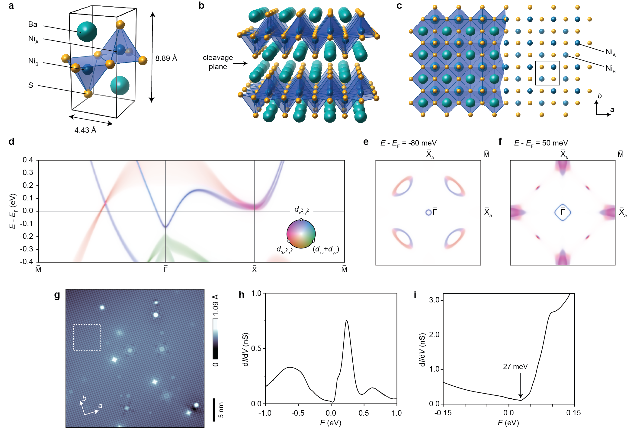
Properties of the surface
BaNiS2 is a layered quasi-2-D material with a structure belonging to the nonsymmorphic space group , with lattice parameters reported as = = 4.43 Å and = 8.89 Å [21]. Its structure is composed of NiS5 pyramids whose orientation alternates about the basal plane, and whose basal edges are shared with their neighbors, as depicted in Fig. 1(a). Sandwiching these layers are Ba atoms located between, and almost in the plane of, the apical S of the NiS5 pyramids. As indicated in Fig. 1(b), cleavage can occur between adjacent BaS layers revealing (001) facets. A top-down view of the surface lattice is shown in Fig. 1(c). The cutaway on the right-hand side of the image shows the NiA and NiB lattices.
Figure 1(d) shows the (001) surface spectral function along chosen high-symmetry axes of the BZ. The orbital composition of the bands are shown using hue as indicated in the inset. Approximately halfway along the line, there exists a Dirac cone. This feature represents the surface projection of a 3-D cone emanating from one of the four Dirac nodal-lines running between the and planes [13]. The electron-like pocket surrounding the -point results from a feature previously described as a pinched electron-like tube connecting the faces of the BZ [23]. A third noteworthy feature is the electron-like band centered around the point. This results from the collapse into two dimensions of a band surrounding each of the R points at the edges of the bulk BZ, and the previously described Rashba splitting within these bands is also observed here [24, 25].
In Fig. 1(e) we show a constant-energy cross-section taken from at = -80 meV. Here the electron-like pocket around the bulk point, and hole-pockets stemming from the Dirac nodal-lines, are seen to collapse into a circle and a set of ellipses, respectively, in the surface BZ. The Dirac cones are composed of a hybridization of the Ni and orbitals. Below the Dirac points, these orbitals contribute the inner (-facing) and outer (-facing) arcs, respectively [13], and this is reversed above the Dirac points as seen at the left-hand-side of Fig. 1(d). Fig. 1(f) shows a constant-energy cross-section at = 50 meV, an energy which coincides closely with both the Dirac nodes and the bottom of the electron bands around the point. Like the Dirac cones, these bands are composed of a hybridization of and orbitals. We point out that these numerical calculations do not accurately reflect the energies of these features, which are to be properly established through observations presented below (and to some extent in the Supplemental Information).
A typical constant-current STM topography image acquired at a cleaved surface is shown in Fig. 1(g). The observed atomic corrugations almost certainly represent the Ni square net, and specifically NiA. (The periodicity of the corrugations corresponds to one observed atom per surface unit cell – see Supplemental Information.)
Figures 1(h) and 1(i) show typical tunneling conductance curves, denoted by , where by convention ( being the electron charge and the sample bias). These are averaged over the nm2 field of view marked as a white dashed square in Fig. 1(g). The curves indicate a density of states close to an ideal semimetal, i.e. becoming small near the Fermi energy. In Fig. 1(i), the ‘v’-shaped minimum at 27 meV can be taken to indicate the approximate energy of the Dirac crossings. The shallow and roughly linear onset toward lower energy likely corresponds to Dirac cones emerging from these crossings. Additional spectroscopy measurements acquired under magnetic fields are shown in the Supplementary Information. These indicate the emergence of a field-independent Landau level, indicating a Berry’s phase of associated with each Dirac point, as well as giving a more precise estimate of the Dirac points’ energy. We note that is located near the Dirac point energy, where the density-of-states is minimal. This situation would generally be unfavorable for an electronic instability. However, as we will show below, BaNiS2 exhibits a likely correlation-driven electronic nematicity.
Observation of nematic order
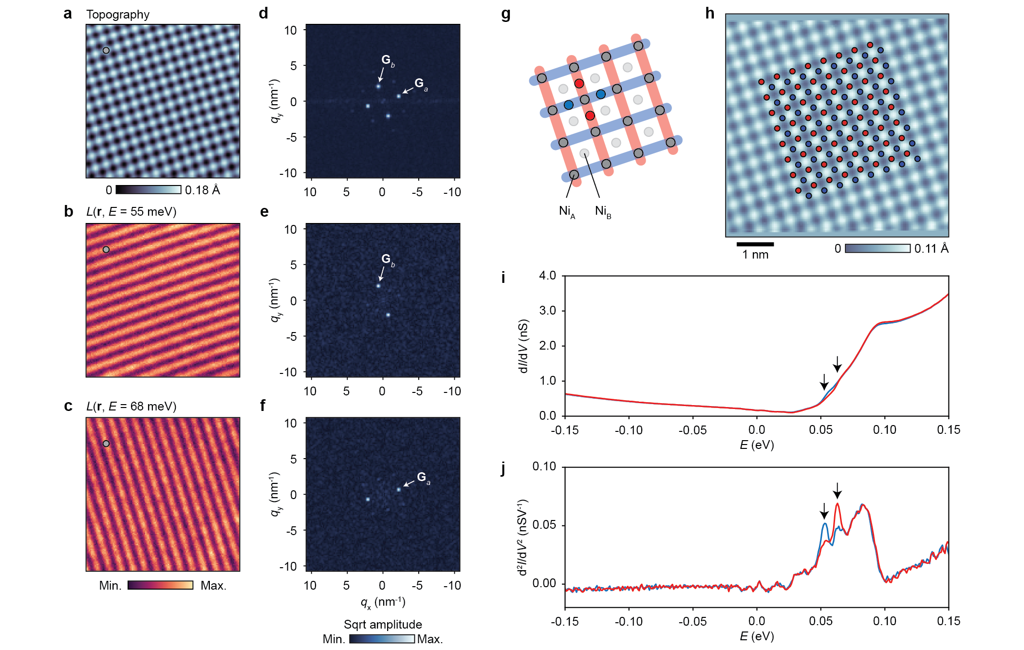
Figure 2 shows high-resolution spectroscopic imaging that reveals an unexpected symmetry breaking within the local density-of-states. Figure 2(a) shows STM topography over the same nm2 field of view as marked by a white dashed square in Fig. 1(g). A gray dot in the upper left-hand corner marks one of the NiA sites for a point of reference. Differential conductance was acquired by measuring a curve at each pixel. Figures 2(b) and 2(c) show images extracted from the normalized differential conductance defined as , at = 55 meV and 68 meV, respectively. The normalization mitigates the so-called ‘set-point effect’ [26], an unwanted influence of variations in tip-sample spacing on images. The gray dots in Figs 2(b) and 2(c) are carried over from the one in Fig. 2(a). The Fourier transform images of the topographic and images are shown in Figs. 2(d–f). In Fig. 2(d) the peaks corresponding to the reciprocal lattice vectors and are seen, and show the expected symmetry. In Figs. 2(b) and 2(c), we see the two symmetry stripe patterns, each commensurate with, and in phase with, one of the surface lattice corrugations [i.e. for each pattern as seen in Figs 2(e) and (f)].
The peaks in intensity of each striped pattern correspond directly with the rows or columns of the NiA lattice, and each stripe lies along a NiA–NiA bond chain (or more strictly, a NiA–S–NiA bond chain). Figure 2(g) shows a cartoon of this situation, in which the blue (red) stripes indicate the pattern at the lower (upper) energy. As well as the in-plane projections of the NiA and NiB sites, the sites belonging to the two inequivalent bond-centered lattices are also shown, with red and blue dots. As shown in Fig. 2(h) we perform a sampling of the raw conductance data in the same field of view as Figs. 2(a–c), on a 88 grid on each of the sublattices. Figure 2(i) shows the resulting curves (averaged over the 64 sites of each grid). In each curve, a subtle shoulder in the steep onset of states above the conductance minimum is marked with a black arrow. A derivative with respect to energy, shown in Fig. 2(j) helps to clarify the difference between the two curves. A peak in the second-derivative of an curve is generally known to correspond to the availability of an additional tunneling channel, such as a band edge that becomes available upon reaching the necessary bias. The energy difference between the peaks in the two curves is 12 meV.
A question that reasonably follows from the above observation is whether a domain structure of the nematic order exists. Throughout this work, examining patterns of nematic order in two samples and searching over fields-of-view up to 500 nm, no domain boundaries were observed, and the order was seen to be preserved across a step-terrace morphology including three atomic terraces (see Supplemental Information).
Manifestation of nematicity in QPI
The mechanism underlying the observed nematic order might be elucidated by examining the momentum-space electronic structure at the BaNiS2 surface, and indirect insights into this can be obtained through interpretations of QPI phenomena. Such measurements can complement previous angle-resolved photo-emission spectroscopy reports [24, 14, 13], but can additionally probe unoccupied bands.
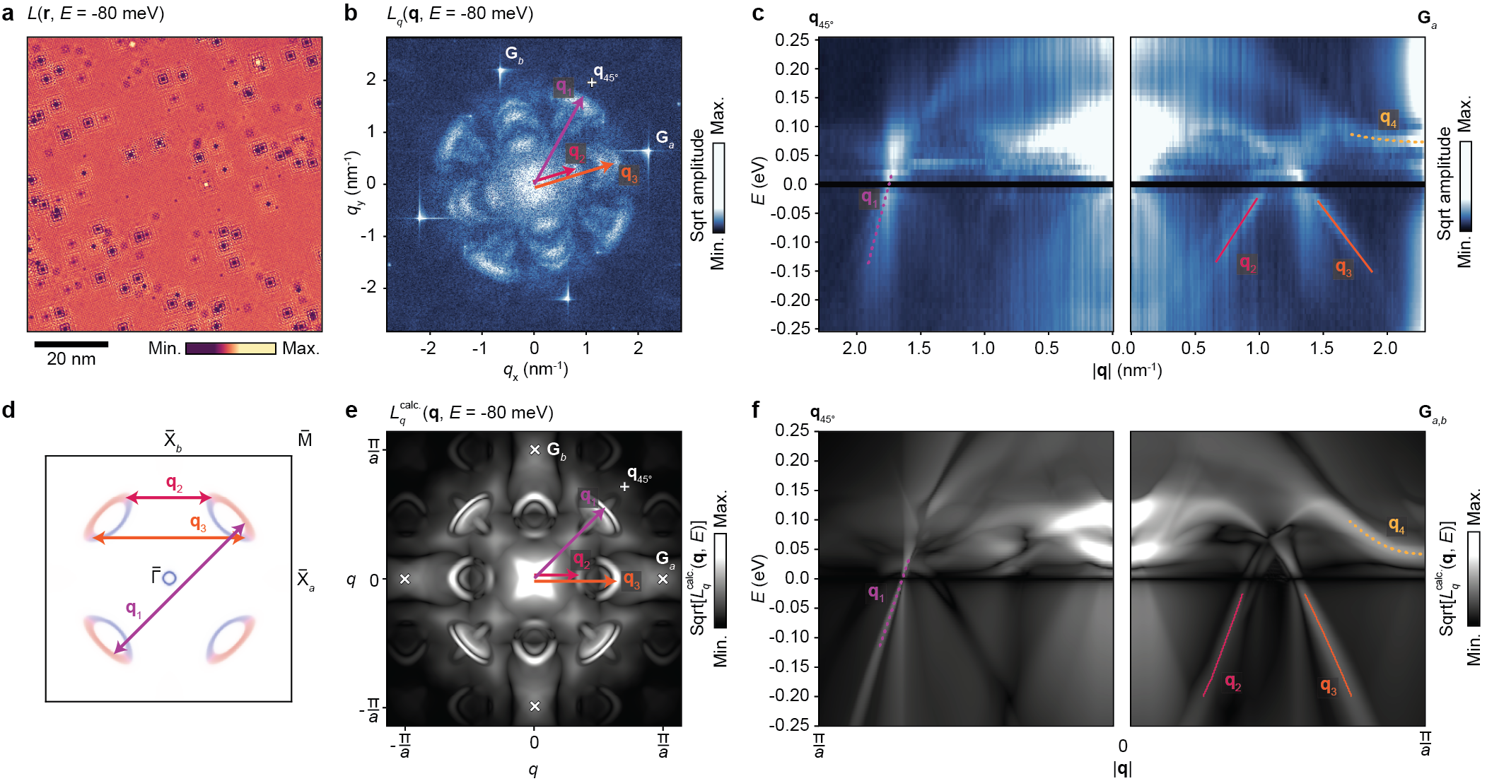
Figure 3(a) shows a selected image from data acquired in a larger field-of-view, at , in which modulations resulting from interference caused by scattering of quasiparticles from point defects are seen. Figure 3(b) shows the Fourier transform . We hereafter refer to such Fourier transformed conductance data loosely as . The reciprocal lattice vectors are again denoted by and . At this energy we identify three prominent scattering vectors, labelled . Figure 3(c) shows linecuts through , running from the origin to , and along a line of the same length running halfway between and . The most interesting features are seen in the linecut running from the origin to . The branches and form an inverted ‘v’ below , and it can be inferred that they represent the shortest and longest possible scattering vectors, respectively, connecting two Dirac cones in adjacent quadrants of the BZ. At positive energy, a branch with apparently very weak dispersion, , extends to meet . This branch will be discussed in greater detail below.
Figure 3(d) shows the likely origin of each of the scattering signals found at = -80 meV. We attribute to scattering between Dirac cones on opposite sides of the BZ. We attribute and to scattering between cones in adjacent quadrants of the BZ, and specifically between the least- and most-distance ends of the respective ellipsoids as illustrated in Fig. 3(d). Figure 3(e) and 3(f), show the corresponding calculated QPI pattern and linecuts. All of the labeled QPI branches are qualitatively reproduced.
Comparing the data shown in Figs. 3(c) and (f), we find that the observed dispersions for and are only a factor of 0.58 as high as the calculated ones. With reference to recent related work, we speculate that the reason could be a failure to fully account for electronic correlations that might renormalize the band dispersion at low energies [27]. Therefore the inferred ‘squeezing’ of the band structure near may reflect significant electronic correlation effects in the real material.
A numerical fitting to the and branches, shown as red and orange solid lines in Fig. 3(c), yields apparent velocities = 8.15 m s-1 and = -6.91 m s-1, respectively. However, these values are related only indirectly to any actual band velocities, since a Fourier transform of QPI modulations visualized the momentum-transfer () space rather than the momentum () space. By making a comparison between the observed and calculated features in -space, and also by making a -space-to--space comparison of the calculation results, we can eventually estimate some key properties of the Dirac cones. (See the Supplemental Information for full arguments.) In this way, the band velocities of the inner (-facing) and outer (-facing) sides of each Dirac cone are estimated to be = 3.09105 m s-1 and = -2.98105 m s-1, respectively. This is reasonably consistent with a rough estimate drawn from recently reported angle-resolved photoemission spectroscopy results, of m s-1 [13].
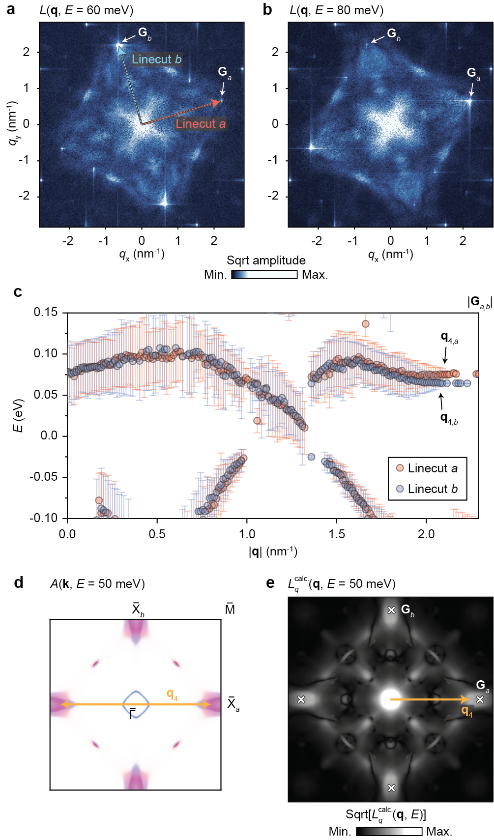
Having identified the -space signatures of the Dirac cones, we turn our attention to the manifestation in QPI phenomena of the nematic behavior described above. Examining the data further, we find that in a small energy range a few tens of meV above there appears a lowering of symmetry similar to that shown in Fig. 2. Two images selected from the same data as shown in Fig. 3, at = 60 meV and = 80 meV, are shown in Figs. 4(a) and 4(b) respectively. Each image shows an asymmetry in intensity between the pairs of reciprocal lattice peaks and [recall Figs. 2(e) and 2(f)].
Figure 4(c) shows the result of fitting a sum of multiple Lorentzian functions to the curve at each -point along the lines from to each of the reciprocal points and . [This is the precursor step to obtaining the linear fits shown in Fig. 3(c), and the full details are described in the Supplemental Information]. The results from each line profile are superimposed along the same axis for comparison. We see that nearly everywhere the peak energies show only small differences, but that a noticeable difference appears as we approach the endpoints . We therefore distinguish between the branches along the two axes by relabeling them as and . As approaches , the energy splitting between the and branches approaches 12 meV. This is consistent with the splitting observed in intra-unit-cell sampling of data shown in Fig. 2. The 10 meV difference in the absolute energies of the two branches as compared to those of the two peaks in Fig. 2(j) is likely due to the fact that the measurements were acquired on two different sample surfaces.
Scattering vectors equal to () in -space serve to connect () and its counterpart at the opposite edge of the BZ. This suggests that the branch captured in Figs 3 and 4 results from scattering between the electron pockets around the .Figures 4(d) and 4(e) depict this scenario with reference to the calculated spectral function, and show the appearance of in the calculated QPI pattern.
Origin of nematicity via the density wave equation
The results presented above describe symmetry-breaking both in the intra-unit cell density-of-states and also in quasiparticle scattering between the pairs of electron-like pockets around opposing and points. We interpret these results as different manifestations of the same underlying phenomenon. The latter manifestation strongly suggests a -dependent shift of the band energies, that has an opposite sign near as compared to , and this would also give an intuitive explanation for the former manifestation: The electron bands flatten out exactly at the points so that the last remaining scattering vectors connecting the pairs of bands at the band bottoms are exactly . The and striped patterns each appear at the energy that the respective band bottoms out. The simplest -dependent energy correction that explains the above results is one with -form factor.
A structural distortion is unlikely as the origin of the observed lifting of degeneracy because BaNiS2 is tetragonal at room temperature, and no phase transition is reported down to T = 2 K [20]. It may be more reasonable to assume an electronic origin. We exclude a simple orbital ordering however, because there is apparently no degeneracy of the relevant orbitals that make up the pocket around the points (as among and , for example). Moreover, the small density-of-states near likely excludes mechanisms stemming from a Fermi-surface-instability.
For these reasons we adopt a framework based on the density wave (DW) equation, which has previously been used to discuss -form factor energy corrections emerging from many-body correlations in the context of the unconventional superconductors [29, 30, 28, 31, 32, 33, 35] as well as exotic density-wave states in other systems [34]. In this scenario, broken symmetry in the charge sector may arise as a many-body correction generated by the interference of spin fluctuations.
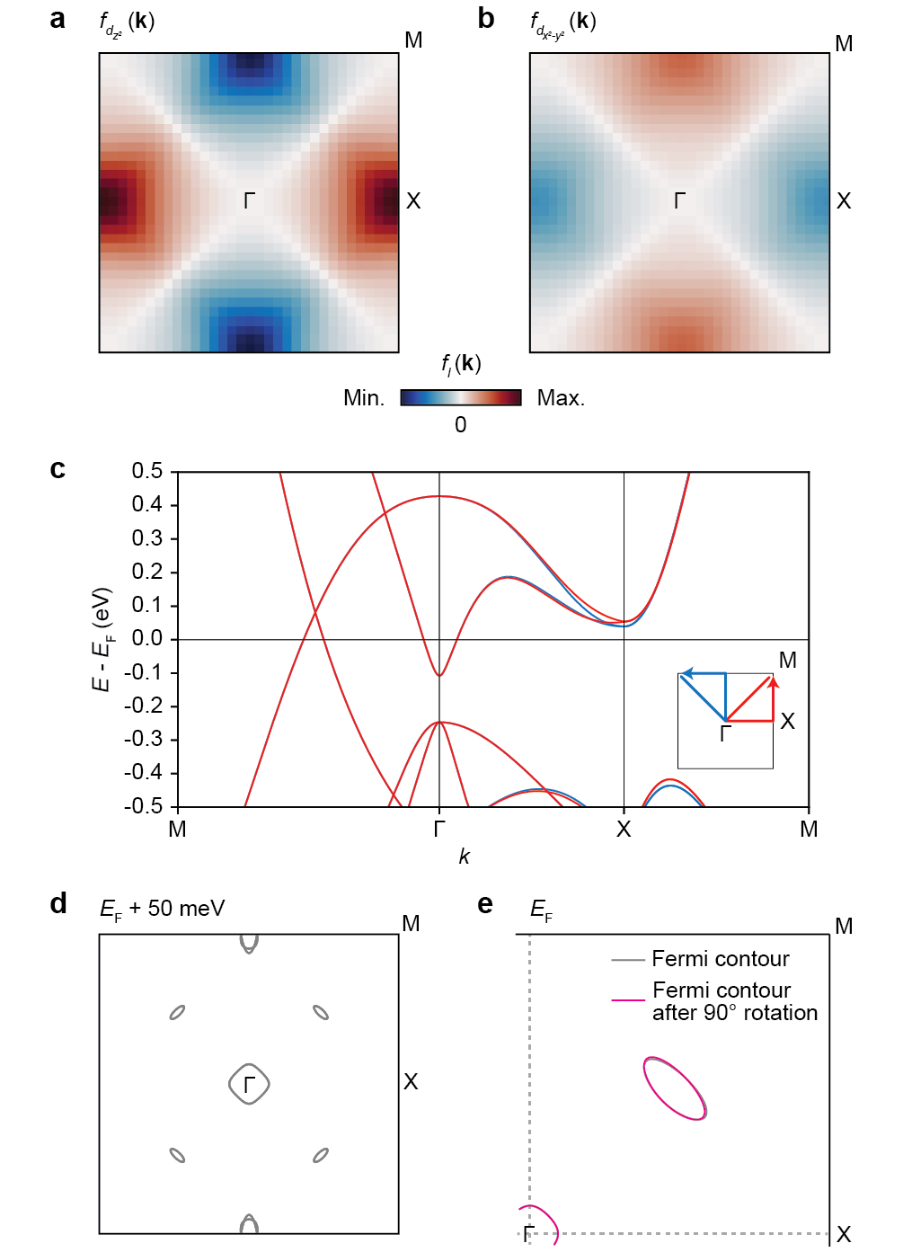
Figure 5 shows results of numerical calculations of -form factor energy corrections . The full details of the calculations are described in the Methods section. Figs. 5(a) and 5(b) show plots of the form factors calculated for the two dominant orbitals of the electron-like band near X, namely and [recall Fig. 2(a) and (c)]. The strength of each is plotted with a common color scale. Although and are related by a sign change and therefore partially cancel each other, the former is a factor of 2 stronger than the latter and a significant -form factor correction remains. Note that an inverse Fourier transform of the -form factor results in a bond-order pattern in real-space, similar to that illustrated in Fig. 2(g). Figure 5(c) shows the resulting band structure after applying the correction to the band energies, sampled along two paths in the BZ whose segments run perpendicular to each other, as shown in the inset. The blue and red curves show negligible difference except in the region near the -point. This difference serves to explain the observations of rotational symmetry breaking in QPI and in high-resolution spectroscopic imaging described in the sections above. Figure 5(d) shows the constant-energy contours of the corrected band structure at the energy of 50 meV, roughly the energy at which nematicity was observed. In Fig. 5(e) we plot one quadrant of the BZ showing the Fermi contour of a Dirac cone, and that of another Dirac cone rotated by 90∘ from an adjacent quadrant. This visualizes the effect of the -form factor correction on the Dirac cones, which is seen to be fairly small. This is because the lines on which the Dirac cones are centered are the nodes of the form factor, as shown in Figs. 5(a) and 5(b).
A discussion of the energy savings originating from the emergence of bond order is given in the Supplemental Information.
Conclusion
To summarize the results of this work, we have characterized the cleaved (001) surface of BaNiS2 using STM, where we can access the electronic properties of the uppermost Ni square net. Through tunneling spectroscopy (including Landau level spectroscopy), we determine the approximate energy of the Dirac nodal-line to be 27 meV. We estimate the Fermi velocities on the inner and outer arcs of each Dirac cone, along the line, as = 3.09105 m s-1 and = -2.98105 m s-1, respectively. This is in fairly good agreement with previous reports [13].
High-resolution conductance imaging and QPI observations both reveal a lowering of symmetry, from the symmetry expected for a material belonging to the space group, to . The configuration consists of a pair of striped patterns appearing at around 60 meV above , related to each other by a 90∘ rotation and 12 meV energy splitting, and oriented along the Ni bond chains. This symmetry-breaking phenomenon appears to respect the translational symmetries of the surface lattice but break its rotational symmetry. Hence it constitutes an example of nematic order.
A plausible explanation for the observed nematicity is the -form factor modification, , to the hopping integrals on the Ni square net, characterized within the DW equation framework as resulting from interference between spin fluctuations. Because the Dirac points lie on the nodes of , they are almost unaffected by the nematicity. An additional unusual feature of nematicity in BaNiS2 is that it is present even in a semimetal, having very low density-of-states at . This is in sharp contrast with mechanisms such as the Peierls-type instability or the band Jahn-Teller effect, which are usually promoted by a large density-of-states at and a correspondingly large available energy saving upon reconfiguration of the Fermi surface.
From the above findings we conclude that, in BaNiS2, topological Dirac nodal-lines and symmetry-breaking electronic correlations coexist without the former being significantly perturbed by the latter. However, looking ahead, the investigation of the BaCo1-xNixS2 solid solution will be of interest because substitution with Co should be expected to increase the influence of electronic correlations on the electronic behavior. Ultimately, this may allow us to observe the fate of topologically protected Dirac cones as the system is driven toward a Mott transition.
Overall, as well as adding to the understanding of the nearly ideal Dirac nodal-line electronic structure of BaNiS2, the observations presented here also advance the general understanding of electronic nematic states in correlated transition metal square lattice systems.
Materials and Methods
STM measurements
Single crystals of BaNiS2 were synthesized as described previously [36, 37]. Samples were prepared for measurement by cleaving in an ultra-high vacuum chamber ( Torr) on a cleaving stage held at about 77 K. They were then quickly inserted into a modified Unisoku 1300 low-temperature STM system held at 1.5 K [38], equipped with a home-made head similar to that described previously [39]. Scanning tips were formed by electrochemically etching tungsten wire, and characterized and conditioned using a field ion microscope and mild indentation at a clean Cu(111) surface. To measure differential conductance , a lock-in technique was used, with modulation frequency = 617.3 Hz. The modulation amplitude used for each measurement, where relevant, is specified in the respective figure caption.
STM data processing
To prepare image data for fast Fourier transformation, one of two methods was used. For all data shown in Fig. 2, a Hann window was applied before transformation. For all imaging of QPI patterns in Figs. 3 and 5, Moisan’s ‘periodic plus smooth image decomposition’ method was used [40]. This avoids the introduction by the Hann window of periodic envelope artifacts in the domain [visible in Fig. S1(b) of the Supplemental Information].
Density functional theory and tight binding model calculations
To model QPI patterns, we first performed density functional theory (DFT) calculations for bulk BaNiS2 using the Perdew-Burke-Ernzerhof exchange-correlation functional [41], as implemented in the WIEN2k package [42]. We also performed additional calculations using a modified Becke-Johnson exchange potential [43] to account for the many-body correlation effects not treatable within DFT. These calculations are referred to as correlation-corrected DFT, or in short CC-DFT. For both sets of calculations, we sampled the bulk BZ using a -mesh and muffin-tin radius for all atoms such that its product with the maximum modulus of reciprocal space becomes . The bulk DFT and CC-DFT calculations were then downfolded into a 20-band tight-binding model using maximally localised Wannier functions [44, 45] incorporating Ni- orbitals as the projection centers. The tight-binding Hamiltonian was then used to construct a 100-layer supercell stacked along the crystalline -axis, while spanning the surface BZ over a fine -mesh.
As the CC-DFT results more successfully reproduced observed electronic structures, most notably the electron-like pocket around the -point in photoemission measurements [13], these were adopted for the comparisons discussed in this work.
Calculations of QPI patterns
With the projected wave functions of the topmost two Ni layers, calculations of QPI were carried out using the T-matrix formalism, in a manner similar to that described previously [46]. The lifetime broadening was chosen to be 1 meV and a localized scalar scatterer with a scattering potential of 0.1 eV in the unitary limit was employed. We performed a basis transformation from the lattice model to the continuum model using the Wannier function [47] constructed from the tight-binding wavefunctions between 1 eV at a height of 1 nm above the NiA plane. Lock-in broadening and normalization according to the integrated density-of-states were included for direct comparison with the experimental results. Simulations were carried out for a scatterer at both NiA and NiB sites, and summed to simulated a random distribution of impurities.
Calculations of d-form factor correction via DW equation.
Based on the 20-band tight binding model derived from the CC-DFT results described above, a 2-D five band tight-binding model was constructed by ignoring inter-layer hopping, ignoring spin, and moving from the ‘folded’ to the ‘unfolded’ BZ. In this way the NiA and NiB sites are treated identically. This model is equivalent to one using the folded BZ if the spin-orbit interaction and inter-layer hopping are both ignored. (The results are displayed in Fig. 5 after returning to the folded BZ.)
With this model as a starting point, and following previous works, the linearized DW equation [28] can then be used to characterize rotational symmetry breaking in the hopping integrals. As in previous treatments, the DW interaction includes the Maki-Thomson, Hartree, and Aslamazov-Larkin terms, the latter of which captures the effects of interference between spin fluctuations, and can contribute a -form factor correction [30]. The interaction is quantified by the momentum-dependent form factor where denotes a particular orbital. With = 0, can describe a uniform bond order as suggested by observation.
We set = 40 meV and / = 0.1, where is the Hund’s coupling and is the on-site Coulomb interaction.
Acknowledgements
We are grateful to T. Machida and A. Gauzzi for helpful discussions. This work was supported by JST CREST Grant No. JPMJCR16F2, and by a Grant-in-Aid for Scientific Research on Innovative Areas ‘Quantum Liquid Crystals’ (KAKENHI Grant No. JP19H05824 and No. JP19H05825) from JSPS of Japan. C.J.B. acknowledges support from RIKEN’s Programs for Junior Scientists.
Author contributions
S. Shamoto synthesized the BaNiS2 crystals. C.J.B. performed all STM measurements and related data processing. M. S. B. performed the DFT and tight-binding calculations and Y. K. performed the subsequent T-matrix calculations of QPI patterns. Y. Y., S. O. and H. K. proposed and calculated the -form factor band correction. T. H. supervized the project. All authors were involved in interpretation of the results. C. J. B. prepared the manuscript with input from all authors.
Data availability
The data that support the findings presented here are available from the corresponding authors upon reasonable request.
References
- [1] B. Keimer and J. E. Moore, The physics of quantum materials. Nature Physics 13, 1045–1055 (2017). https://doi.org/10.1038/nphys4302
- [2] R. Li, J. Wang, X.-L. Qi, and S.-C. Zhang, Dynamical axion field in topological magnetic insulators. Nature Physics 6, 284–288 (2010). https://doi.org/10.1038/nphys1534
- [3] Y. Cao, V. Fatemi, S. Fang, K. Watanabe, T. Taniguchi, E. Kaxiras, and P. Jarillo-Herrero, Unconventional superconductivity in magic-angle graphene superlattices. Nature 556, 43–853 (2018). https://doi.org/10.1038/nature26160
- [4] M. J. Lawler, K. Fujita, J. Lee, A. R. Schmidt, Y. Kohsaka, C. K. Kim, H. Eisaki, S. Uchida, J. C. Davis, J. P. Sethna and E.-A. Kim. Intra-unit cell electronic nematicity of the high- copper-oxide pseudogap states. Nature 466, 347–351 (2010). https://doi.org/10.1038/nature09169
- [5] K. Fujita, M. H. Hamidian, S. D. Edkins, C. K. Kim, Y. Kohsaka, M. Azuma, M. Takano, H. Takagi, H. Eisaki, S. Uchida, A. Allias, M. J. Lawler, E.-A. Kim, S. Sachdev and J. C. S. Davis, Direct phase-sensitive identification of a d-form factor density wave in underdoped cuprates. Proc. Natl. Acad. Sci. 111, E3026–E3032 (2014). https://doi.org/10.1073/pnas.1406297111
- [6] T.-M. Chuang, M. P. Allan, J. Lee, Y. Xie, N. Ni, S. L. Bud’ko, G. S. Boebinger, P. C. Canfield and J. C. Davis, Nematic Electronic Structure in the “Parent” State of the Iron-Based Superconductor Ca(Fe1-xCox)2As2. Science 327, 181–184 (2010). https://doi.org/10.1126/science.1181083
- [7] R. M. Fernandes, A. V. Chubukov and J. Schmalian, What drives nematic order in iron-based superconductors? Nature Physics 10, 97–104 (2014). https://doi.org/10.1038/nphys2877
- [8] S. A. Kivelson, E. Fradkin, and V. J. Emery, Electronic liquid-crystal phases of a doped Mott insulator. Nature 393, 550–553 (1998). https://doi.org/10.1038/31177
- [9] V. Oganesyan, S. A. Kivelson, and E. Fradkin, Quantum theory of a nematic Fermi fluid. Phys. Rev. B 64, 195109 (2001).
- [10] E. Fradkin, S. A. Kivelson, M. J. Lawler, J. P. Eisenstein, and A. P. Mackenzie, Nematic Fermi fluids in condensed matter physics. Ann. Rev. Cond. Mat. Phys. 1, 153–178 (2010). https://doi.org/10.1146/annurev-conmatphys-070909-103925
- [11] L. M. Schoop, F. Pielnhofer, and B. V. Lotsch, Chemical Principles of Topological Semimetals. Chem. Mater. 30, 3155–3176 (2018). https://doi.org/10.1021/acs.chemmater.7b05133
- [12] D. Santos-Cottin, M. Casula, L. de’ Medici, F. Le Mardelé, J. Wyzula, M. Orlita, Y. Klein, A. Gauzzi, A. Akrap, and R. P. S. M Lobo, Optical conductivity signatures of open Dirac nodal lines. Phys. Rev. B 104, L201115 (2021). https://doi.org/10.1103/PhysRevB.104.L201115
- [13] N. Nilforoushan, M. Casula, A. Amaricci, M. Caputo, J. Caillaux, L. Khalil, E. Papalazarou, P. Simon, L. Perfetti, I. Vobornik, P. K. Das, J. Fujii, A. Barinov, D. Santos-Cottin, Y. Klein, M. Fabrizio, A. Gauzzi, and M. Marsi, Moving Dirac nodes by chemical substitution. Proc. Natl. Acad. Sci. 118, e2108617118 (2021). https://doi.org/10.1073/pnas.2108617118
- [14] N. Nilforoushan, M. Casula, M. Caputo, E. Papalazarou, J. Caillaux, Z. Chen, L. Perfetti, A. Amaricci, D. Santos-Cottin, Y. Klein, A. Gauzzi, and M. Marsi, Photoinduced renormalization and electronic screening of quasi-two-dimensional Dirac states in BaNiS2. Phys. Rev. Res. 2, 043397 (2020). https://doi.org/10.1103/PhysRevResearch.2.043397
- [15] D. Mandrus, J. L. Sarrao, B. C. Chakoumakos, J. A. Fernandez-Baca, S. E. Nagler, and B. C. Sales, Magnetism in BaCoS2. J. Appl. Phys. 81, 4620 (1997). https://doi.org/10.1063/1.365182
- [16] S. R. Krishnakumar, T. Saha-Dasgupta, N. Shanthi, Priya Mahadevan, and D. D. Sarma Electronic structure of and covalency driven metal-insulator transition in BaCo1-xNixS2. Phys. Rev. B 63, 045111 (2001). https://doi.org/10.1103/PhysRevB.63.045111
- [17] T. Sato, H. Kumigashira, D. Ionel, T. Takahashi, I. Hase, H. Ding, J. C. Campuzano, and S. Shamoto, Evolution of metallic states from the Hubbard band in two-dimensional Mott system BaCo1-xNixS2. Phys. Rev. B 64, 075103 (2001). https://doi.org/10.1103/PhysRevB.64.075103
- [18] Z. Guguchia, B. A. Frandsen, D. Santos-Cottin, S. C. Cheung, Z. Gong, Q. Sheng, K. Yamakawa, A. M. Hallas, M. N. Wilson, Y. Cai, J. Beare, R. Khasanov, R. De Renzi, G. M. Luke, S. Shamoto, A. Gauzzi, Y. Klein, and Y. J. Uemura, Probing the quantum phase transition in Mott insulator BaCoS2 tuned by pressure and Ni substitution. Phys. Rev. Materials 3, 045001 (2019). https://doi.org/10.1103/PhysRevMaterials.3.045001
- [19] E. C. Schueller, K. D. Miller, W. Zhang, J. L. Zuo, J. M. Rondinelli, S. D. Wilson, and R. Seshadri, Structural signatures of the insulator-to-metal transition in BaCo1-xNixS2. Phys. Rev. Materials 4, 104401 (2020). https://doi.org/10.1103/PhysRevMaterials.4.104401
- [20] D. Santos-Cottin, A. Gauzzi, M. Verseils, B. Baptiste, G. Feve, V. Freulon, B. Plaçais, M. Casula, and Y. Klein, Anomalous metallic state in quasi-two-dimensional BaNiS2. Phys. Rev. B 93, 125120 (2016). https://doi.org/10.1103/PhysRevB.93.125120
- [21] I. E. Grey and H. Steinfink, Crystal structure and properties of barium nickel sulfide, a square-pyramidal nickel(II) compound. J. Am. Chem. Soc. 92, 17, 5093–5095 (1970). https://doi.org/10.1021/ja00720a015
- [22] K. Momma and F. Izumi, VESTA 3 for three-dimensional visualization of crystal, volumetric and morphology data. J. Appl. Crystallogr. 44, 1272–1276 (2011). https://doi.org/10.1107/S0021889811038970
- [23] Y. Klein, M. Casula, D. Santos-Cottin, A. Audouard, D. Vignolles, G. Fève, V. Freulon, B. Plaçais, M. Verseils, H. Yang, L. Paulatto, and Andrea Gauzzi, Importance of nonlocal electron correlation in the BaNiS2 semimetal from quantum oscillations studies. Phys. Rev. B 97, 075140 (2018). https://doi.org/10.1103/PhysRevB.97.075140
- [24] D. Santos-Cottin, M. Casula, G. Lantz, Y. Klein, L. Petaccia, P. Le Fèvre, F. Bertran, E. Papalazarou, M. Marsi, and A. Gauzzi, Rashba coupling amplification by a staggered crystal field. Nat. Commun. 7, 11258 (2016). https://doi.org/10.1038/ncomms11258
- [25] J. Sławińska, A. Narayan, and S. Picozzi, Hidden spin polarization in nonmagnetic centrosymmetric BaNiS2 crystal: Signatures from first principles. Phys. Rev. B 94, 241114 (2016). https://doi.org/10.1103/PhysRevB.94.241114
- [26] Y. Kohsaka, C. Taylor, K. Fujita, A. Schmidt, C. Lupien, T. Hanaguri, M. Azuma, M. Takano, H. Eisaki, H. Takagi, S. Uchida, and J. C. Davis, An Intrinsic Bond-Centered Electronic Glass with Unidirectional Domains in Underdoped Cuprates. Science 315, 1380–1385 (2007). https://doi.org/10.1126/science.1138584
- [27] J. Fujioka, R. Yamada, M. Kawamura, S. Sakai, M. Hirayama, R. Arita, T. Okawa, D. Hashizume, M. Hoshino, and Y. Tokura, Strong-correlation induced high-mobility electrons in Dirac semimetal of perovskite oxide. Nat. Commun. 10, 362 (2019). https://doi.org/10.1038/s41467-018-08149-y
- [28] K. Kawaguchi, Y. Yamakawa, M. Tsuchiizu and H. Kontani, Competing Unconventional Charge-Density-Wave States in Cuprate Superconductors: Spin-Fluctuation-Driven Mechanism. J. Phys. Soc. Jpn. 86, 063707 (2017). https://doi.org/10.7566/JPSJ.86.063707
- [29] S. Onari and H. Kontani, Self-consistent Vertex Correction Analysis for Iron-based Superconductors: Mechanism of Coulomb Interaction-Driven Orbital Fluctuations. Phys. Rev. Lett. 109, 137001 (2012). https://doi.org/10.1103/PhysRevLett.109.137001
- [30] S. Onari, Y. Yamakawa, and H. Kontani, Sign-Reversing Orbital Polarization in the Nematic Phase of FeSe due to the Symmetry Breaking in the Self-Energy. Phys. Rev. Lett. 116, 227001 (2016). https://doi.org/10.1103/PhysRevLett.116.227001
- [31] S. Onari and H. Kontani, Origin of diverse nematic orders in Fe-based superconductors: rotated nematicity in AFe2As2 (A = Cs, Rb). Phys. Rev. B 100, 020507(R) (2019). https://doi.org/10.1103/PhysRevB.100.020507
- [32] K. Ishida, M. Tsujii, S. Hosoi, Y. Mizukami, S. Ishida, A. Iyo, H. Eisaki, T. Wolf, K. Grube, H. v. L ohneysen, R. M. Fernandes, and T. Shibauchi, Novel electronic nematicity in heavily hole-doped iron pnictide superconductors. Proc. Natl. Acad. Sci. 117, 6424 (2020). https://doi.org/10.1073/pnas.1909172117
- [33] S. Onari and H. Kontani, Hidden antiferronematic order in Fe-based superconductor BaFe2As2 and NaFeAs above . Phys. Rev. Res. 2, 042005(R) (2020). https://doi.org/10.1103/PhysRevResearch.2.042005
- [34] R. Tazai, Y. Yamakawa, S. Onari, and H. Kontani, Mechanism of exotic density-wave and beyond-Migdal unconventional superconductivity in kagome metal AV3Sb5 (A = K, Rb, Cs). Science Advances 8, eabl4108 (2022). https://doi.org/10.1126/sciadv.abl4108
- [35] R. Tazai, S. Matsubara, Y. Yamakawa, S. Onari, and H. Kontani, A Rigorous Formalism of Unconventional Symmetry Breaking in Fermi Liquid Theory and Its Application to Nematicity in FeSe. arXiv:2205.02280 (2022). https://doi.org/10.48550/arXiv.2205.02280
- [36] S. Shamoto, S. Tanaka, E. Ueda, and M. Sato, Single crystal growth of BaNiS2. Journal of Crystal Growth 154, 197–201 (1995). https://doi.org/10.1016/0022-0248(95)00225-1
- [37] S. Shamoto, S. Tanaka, E. Ueda, and M. Sato, Single crystal growth of BaCo1-xNixS2. Physica C 263, 550 (1996). https://doi.org/10.1016/0921-4534(95)00729-6
- [38] T. Hanaguri, Development of high-field STM and its application to the study on magnetically tuned criticality in Sr3Ru2O7. J. Phys. Conf. Ser. 51, 514 (2006). https://doi.org/10.1088/1742-6596/51/1/117
- [39] T. Machida, Y. Kohsaka, and T. Hanaguri, A scanning tunneling microscope for spectroscopic imaging below 90 mK in magnetic fields up to 17.5 T. Rev. Sci. Instrum. 89, 093707 (2018). https://doi.org/10.1063/1.5049619
- [40] L. Moisan, Periodic Plus Smooth Image Decomposition. Journal of Mathematical Imaging and Vision 39, 161–179 (2011). https://doi.org/10.1007/s10851-010-0227-1
- [41] J. Perdew, K. Burke, and M. Ernzerhof, Generalized Gradient Approximation Made Simple Phys. Rev. Lett. 77, 3865 (1996). https://doi.org/10.1103/PhysRevLett.77.3865
- [42] P. Balaha et al., WIEN2K package, Version 13.1, 2013.
- [43] F. Tran and P. Blaha, Accurate Band Gaps of Semiconductors and Insulators with a Semilocal Exchange-Correlation Potential. Phys. Rev. Lett. 102, 226401 (2009). https://doi.org/10.1103/PhysRevLett.102.226401
- [44] I. Souza, N. Marzari, and D. Vanderbilt, Maximally localized Wannier functions for entangled energy bands. Phys. Rev. B 65, 035109 (2001). https://doi.org/10.1103/PhysRevB.65.035109
- [45] [5] A. A. Mostofi, J. R. Yates, Y.-S. Lee, I. Souza, D. Vanderbilt, and N. Marzari, wannier90: A tool for obtaining maximally-localised Wannier functions. Comput. Phys. Commun. 178, 685 (2008). https://doi.org/10.1016/j.cpc.2007.11.016
- [46] Y. Kohsaka, T. Machida, K. Iwaya, M. Kanou, T. Hanaguri, and T. Sasagawa, Spin-orbit scattering visualized in quasiparticle interference. Phys. Rev. B 95, 115307 (2017). https://doi.org/10.1103/PhysRevB.95.115307
- [47] P. Choubey, T. Berlijn, A. Kreisel, C. Cao, and P. J. Hirschfeld, Visualization of atomic-scale phenomena in superconductors: Application to FeSe. Phys. Rev. B 90, 134520 (2014). https://doi.org/10.1103/PhysRevB.90.134520