Modeling the Charge Collection Efficiency in the Li-diffused Inactive Layer of P-type High Purity Germanium Detector
Abstract
A model of the Li-diffused inactive layer in P-type high purity germanium detectors is built to describe the transportation of charge carriers and calculate the charge collection efficiency therein. The model is applied to calculate charge collection efficiency of a P-type point-contact germanium detector used in rare event physics experiments and validated in another P-type semi-planar germanium detector. The calculated charge collection efficiency curves are well consistent with measurements for both detectors. Effects of the Li doping processes on the charge collection efficiency are discussed based on the model. This model can be easily extended to other P-type germanium detectors, for instance, the P-type broad-energy Ge detector, and the P-type inverted-coaxial point-contact detector.
keywords:
P-type germanium detector, Inactive layer, Charge collection efficiency1 Introduction
With excellent energy resolution, high detection efficiency, and extremely low intrinsic background, high purity germanium detectors (HPGe) have been widely used in radiation detection, nuclear physics, particle physics, and astrophysics [1, 2, 3]. The P-type high purity germanium detector with a Li-diffused layer on the surface has been used to search for rare processes, for instance dark matter detection [4]-[8], and the neutrinoless double-beta decay [9, 10].
Fabricated by lithium diffusion technology, the surface N+ layer of the HPGe detector has been recognized to have incomplete charge collection and therefore is referred to as an inactive or dead layer [11, 12, 13]. Measurements of the signals originating in the inactive layer suggest a two-layer structure: a total dead layer near the detector surface where no charge is collected, and a transition layer where charge collections are incomplete, induced signals are with characteristic time features [13, 14].
For the P-type HPGe detector used in rare events searching experiments, the inactive layer serves as a passive shield against the surface contaminations of the detector but reduces the active volume and produces potential backgrounds from the incomplete charge collection signals [13, 15]. Therefore, knowledge of the thickness and structure of the inactive layer is important for correcting the detector’s active volume and understanding the backgrounds.
Measurement of the inactive layer thickness has been discussed in literature [11, 12, 16]. The diffusion and recombination of charge carriers were considered in [15, 21] to model the charge collection efficiency (CCE). In our previous works, the inactive layer of a 1-kg P-type point-contact Ge (PPCGe) detector (CDEX-1B) has been studied [4, 16]. A full charge collection depth (FCCD) of 850120 m was measured using 133Ba calibration source [16]. An empirical CCE function of the lateral inactive layer has been computed using calibration data and Monte Carlo simulation, details of the construction of the empirical CCE function can be found in [16].
In this work, a 1-D model based on first principle is built to calculate the CCE in the inactive layer of the P-type HPGe detector. Our model includes a charge carrier mobility model, a simplified recombination model, and calculations of the electric fields in the inactive layer to model the diffusion, drift, and recombination of charge carriers and calculate the CCE in the inactive layer. Our 1-D model dose not consider the self repulsion of charge carriers. The model is applied to calculate the CCE in the inactive layer of the CDEX-1B PPCGe detector and validated in a P-type semi-planar Ge detector (PSPGe). The effects of detector fabrication process on the inactive layer are also discussed based on the model.
2 The inactive layer model of a P-type HPGe detector
The N+ surface of a P-type HPGe detector can be formed by doping donor impurities (Li) on the surface. The pn-junction is generated near the detector surface when a reverse bias voltage is applied. Full depleted regions are formed both on the P-type and N-type regions and leave a non-depleted neutral N-type region on the surface, as shown in Fig.1.
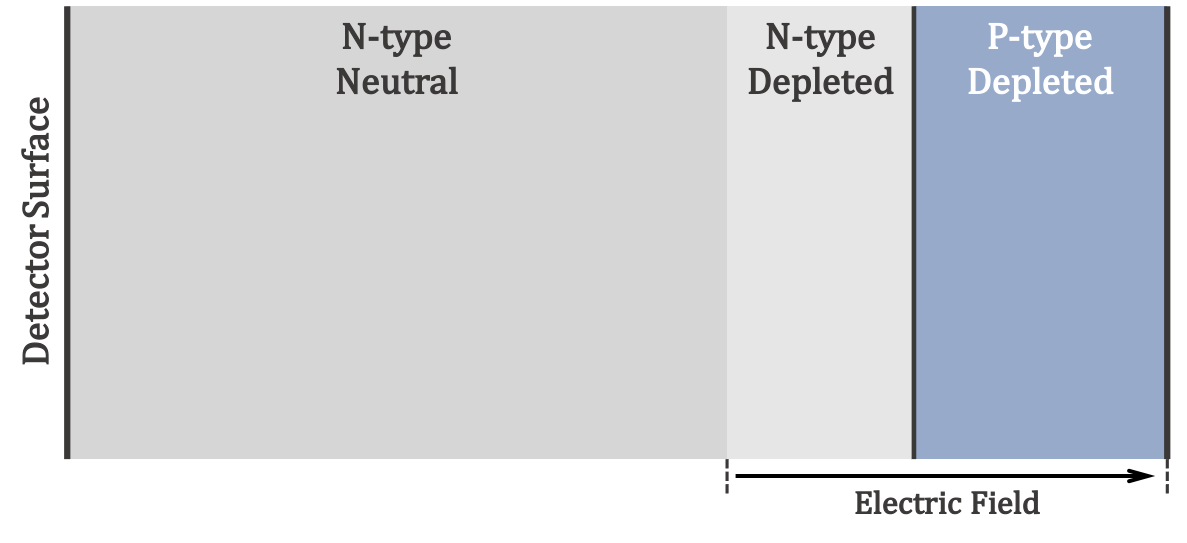
Charge carriers, holes, and electrons are created when energy depositions happen in the germanium crystal. Signals are generated by the charge carriers as they move in the weighted potential field of the p+ readout electrode [17, 18]. Due to the small contact size of the PPCGe detector and the P-type semi-planar Ge detector, majorities of the output signals are formed by holes when they drift near the p+ electrode [19]. Therefore, for charge carriers generated in the surface N-type region, only holes collected by the electric fields in the depleted region can drift to the p+ electrode and form a signal, a fraction of the holes will be trapped or recombined in the N-type region and cause an incomplete charge collection.
The number of produced charge carriers in semiconductor Ge is at for a (MeV) scale energy deposition. Although scattering and absorption of single holes are stochastic, for a large number of holes, their transportations in the N-type layer can be modeled by a transportation equation:
| (1) |
Where is the density of holes. The change rate of hole density () is determined by three processes: (i) the diffusion of holes (): the diffusion coefficient and the second spatial gradient of hole density, (ii) the drift of holes (): the mobility of holes, the spatial gradient of electric field and hole density p, (iii) the termination of holes (), is the hole average lifetime.
2.1 Li concentration profile
During the fabrication of the Li-diffused layer, Li atoms are deposited on the surface of the Ge crystal by evaporation or electrolytic processes [20, 21, 22]. Then the crystal is heated in an annealing process to facilitate the diffusion of Li atoms into the Ge lattice. The concentration profile of Li impurities () depends on the annealing temperature (), annealing time (), and surface concentration (, usually saturated and equal to the solubility of Li in germanium). The Li concentration profile is modeled by an erfc function [23]:
| (2) |
| (3) |
Where x is the depth into the crystal surface. is the diffusivity of Li in germanium in the unit of cm, R is the gas constant (R=1.98 cal/K). and H are diffusivity constant and activation energy, respectively. Their values are taken from measurements by Fuller: for in 473873 K and 8731273 K, as cm2/s and cm2/s, as 11800 cal and 10700 cal, respectively [23, 24].
Figure.2 demonstrates a typical Li concentration profile in the crystal surface layer. Assuming the annealing is carried out in 573 K for 45 minutes, the saturated concentration of Li in Ge at this temperature is cm-3 [25]. The Li concentration profile is calculated via Eq.2 and yields a 1065 m thick N-type layer for a typical acceptor density of cm-3.

2.2 Electric fields in the N-type layer
When a reversed bias voltage is applied in the P-type HPGe detector, the P-type and a part of the N-type region near the detector surface are fully depleted. In the depleted region, the electric fields remove electrons and holes and leave the ionized impurities as space charges. The space charges and the applied bias voltage form electric fields in the N-type depleted region. The electric fields are calculated via solving the Poisson equation and taking the electric field at the pn-junction () as the boundary condition:
| (4) |
Where is the pn-junction depth in the crystal surface, is the concentration of the ionized acceptor impurity, q is the unit charge (q=1.6×10⁻¹⁹ C), and is the dielectric constant of Ge. The left panel of Fig.3 shows the electric fields in the N-type region using the Li profile in Fig.2 and assuming a of 1000 V/cm. The rapid decrease of the electric field near the full depletion depth (FDD) is mainly due to the steep profile of Li concentration and leaving the majority of the N-type region as a neutral layer without electric fields.

2.3 Hole mobility and lifetime
The hole charge drift mobility depends on the scattering of charge carrier holes by the impurity atoms and defects in Ge crystal. Three scattering processes are considered the main contributors to the hole charge drift mobility: ionized impurity scattering, neutral impurity scattering, and acoustic phonon scattering [26]. Other scattering processes, e.g., the optical phonon scattering and the defects scattering, are negligible compared to the three dominant processes for a P-type HPGe detector at a low-temperature working condition [26], therefore are not considered in the calculation of .
The ionized impurity scattering mobility is calculated by the BH model [27], the neutral impurity scattering mobility by Sclar’s work [28], and the acoustic phonon scattering mobility by the Bardeen and Shockley’s model [29]. All constants in the equations are replaced with their corresponding values, and the hole charge drift mobility can be expressed as:
| (5) |
| (6) |
| (7) |
| (8) |
Where the , , , and are in cm2/V/s. and are the densities of ionized and neutral impurity (cm-3), respectively. T is the temperature of Ge crystal (K). A flat profile of neutral impurity is assumed in this work, and is calculated by matching with the IEEE standard 4.2104 cm2/V/s [30] in the P-type region. The right panel of Fig.3 demonstrates the hole charge drift mobility versus the depth into the surface, taking the Li concentration profile in Fig.2. Near the surface of the detector, decreases significantly as the concentration of ionized impurity Li increases.
The diffusion coefficient can be calculated by via the Einstein relation: . Where is the Boltzmann constant, and T is the crystal temperature. In the N-type surface layer, holes may be trapped by the impurities and vanish in various recombination processes before they are collected by the electric fields and transported to the P-type region [31]. Due to unclear types and concentration profiles of the trapping and recombination centers, a constant hole lifetime in the N-type layer and immediate recombination at the detector surface are assumed in this work. The effects of the electric field in the depleted region is evaluated by setting proportional to electric field (maximum set to 100 s), the charge collection efficiency (CCE) is similar to that from a constant . The differences in CCEs are within 0.6%. For a given detector, can be decided by comparing the calculated charge collection efficiency with measurements.
2.4 Calculation of charge collection efficiency
The charge collection efficiencies in different depths of the N-type layer can be calculated by solving Eq(1) via a numerical method. The parameters needed to solve Eq(1) are discussed in Sec2.12.3 and are listed in Table 1.
| Parameter | Type | Note |
|---|---|---|
| Anneal temperature () | Pre-Set | Detector specified, |
| typically 473 K 673 K | ||
| Anneal time () | Pre-Set | Detector specified, |
| Li surface concentration () | Calculated | Solubility of Li in Ge at |
| Acceptor impurity | Pre-Set | Detector specified |
| (1010 cm-3) | ||
| Crystal temperature () | Pre-Set | Detector specified, |
| typically 77 K 90 K | ||
| Electric field | Pre-Set | Determined by the bias |
| at the pn-junction () | voltage and geometry | |
| Electric field () | Calculated | By Li profile and electric field |
| at pn-junction | ||
| Hole Mobility () | Calculated | By Li profile |
| Diffusion Coefficient () | Calculated | By mobility |
| Hole lifetime () | Pre-Set | Detector specified, |
As the collection of holes mainly depends on the maximum depth holes can reach before they are trapped or recombined, the Eq.1 is processed into a 1-D differential equation:
The is the hole density of bin at time , describes the diffusion of holes, describes the drift of holes, and is the fraction of holes been trapped or recombined in the ith bin during times. The Eq.2.4 is calculated with a space bin-size of 20 m and a time bin-size of 0.1 ns.
The solving of Eq.2.4 starts with the injection of holes at depth , and the rest of bins are set as empty. During the transportation, holes reaching the deepest bin (located at the pn-junction) are removed and counted as collected. The CCE of depth is calculated as the ratio of holes collected during the signal forming time of the detector.
3 Result and discussion
3.1 Charge collection efficiency of the CDEX-1B detector
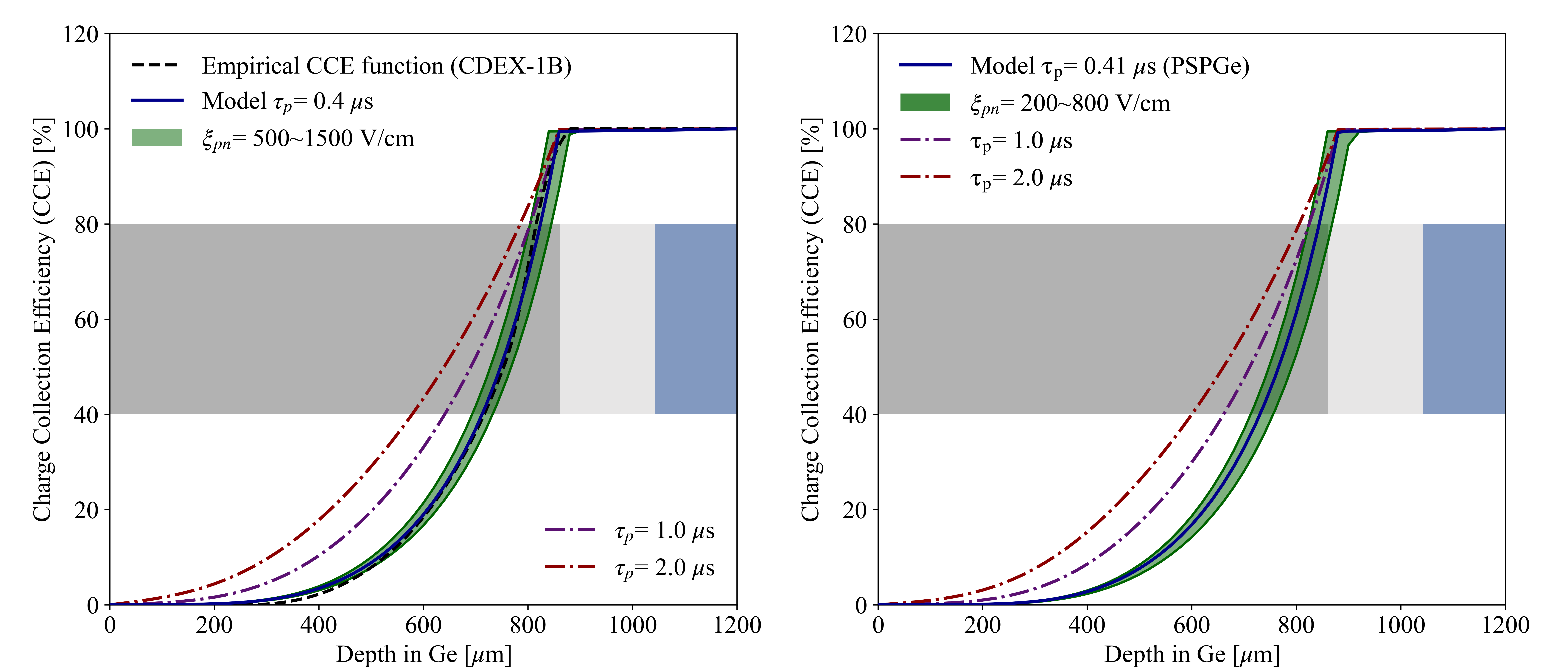
The inactive layer model is applied to the CDEX-1B detector to calculate the CCE function. The model parameters specified for the CDEX-1B detector are listed in Table2. The annealing process can be carried out in wide ranges of temperature (473 673 K) and time (a few minutes several hours) depending on the process [21, 22, 32, 33]. We take a typical 573 K annealing temperature and 45 minutes of annealing time for the CDEX-1B detector. The are taken as the saturated concentration of Li in Ge at 573 K [25]. The acceptor impurity in the detector is evaluated in our previous work [34] by matching the simulated pulse with measurement. An average acceptor impurity of 1.391010 cm-3 in the N-type layer is adopted. According to an electric field simulation [34, 35], the electric fields () are in the range of 500 to 1500 V/cm for the lateral surface of the CDEX-1B detector. The hole lifetime () in the inactive layer is in (ns)(s) scale for a typical P-type HPGe detectors[21, 22]. We run a scan of () in 1 ns5 s range, and the modeled CCE functions of different () are compared with the empirical function. The best match result corresponds to a hole lifetime of 0.40 s.
| Parameter | CDEX-1B | PSPGe |
|---|---|---|
| Anneal temperature () | 573 K | 623 K |
| Anneal time () | 45 min | 18 min |
| Li surface concentration (Cs) | 6.81016 cm-3 | 1.21017 cm-3 |
| Acceptor impurity | 1.391010 cm-3 | 0.301010 cm-3 |
| Crystal temperature (T) | 90 K | 90 K |
| Electric field at pn-junction () | 1000500 V/cm | 500300 V/cm |
| Hole lifetime () | 0.40 s | 0.41 s |
The calculated CCE function is shown with the empirical function in Fig.4 The best-matched result with =1000 V/cm yields a full charge collection depth (99% CCE) of 859 m. The uniformity of the inactive layer thickness is evaluated by the variations of electric field . For in 5001500 V/cm, the corresponding FCCDs are in the range of 839884 m and are consistent with the result from the previous measurement (850120 m). The CCEs calculated by the inactive model and the empirical function are also in good agreement.
3.2 Model validation in a P-type semi-planar HPGe detector
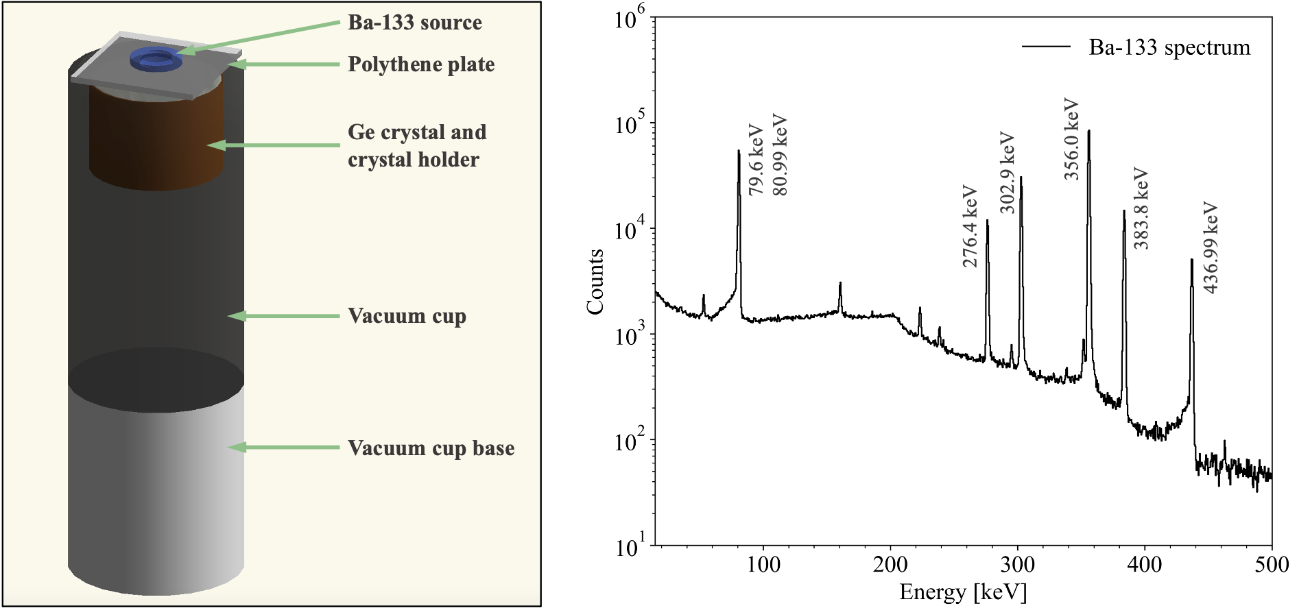
The inactive layer model is applied to a P-type semi-planar Ge (PSPGe) detector purchased from ORTEC. The detector crystal has a diameter of 80 mm, a height of 42.6 mm and a small size p+ contact. The crystal surface is formed by a Li-diffused N-type layer. The thickness of the surface inactive layer is measured by a Ba-133 source following the method described in [16]. Fig.5 shows the setup of the measurement and the measured spectrum of the Ba-133 source. The measured FCCD is 87067 m.
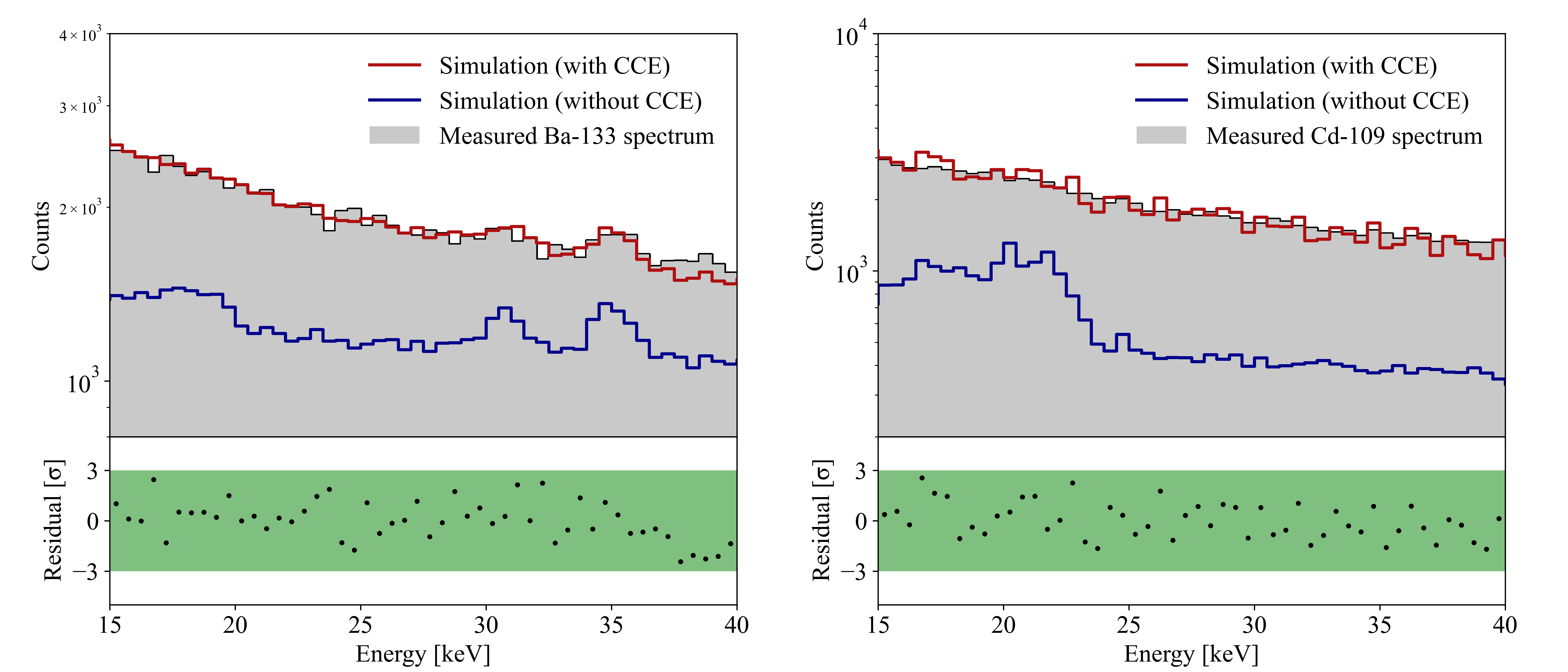
The charge collection efficiency (CCE) is calculated for the PSPGe detector using the parameters listed in Table.2 and shown in Fig.4. Simulated spectra are generated using GEANT4[36] and the calculated CCE: energy depositions in the inactive layer are corrected by the CCE according to their positions. The hole lifetime () is estimated by comparing the simulated spectra with the measured one, and the best matched is 0.41 s for =500 V/cm. The calculated FCCDs are 879 m for =500 V/cm and 859918 m for in range of 200800 V/cm. As shown in Fig.6, simulated spectra of Ba-133 and Cd-109 sources after CCE correction are in good agreement with measurements in 1530 keV region where the spectrum shape is significantly affected by the incomplete charge collection in the inactive layer.
3.3 Effects of Li doping processes on the charge collection efficiency
The annealing time and temperature varies for different Li doping processes [21, 22]. To assess the influence of different annealing parameters on the structure and charge collection efficiency of the inactive layer, we calculate the depths of the pn-junction (pn-depth) and the full depleted region (FDD) under different annealing temperatures and times, as shown in Fig.7.
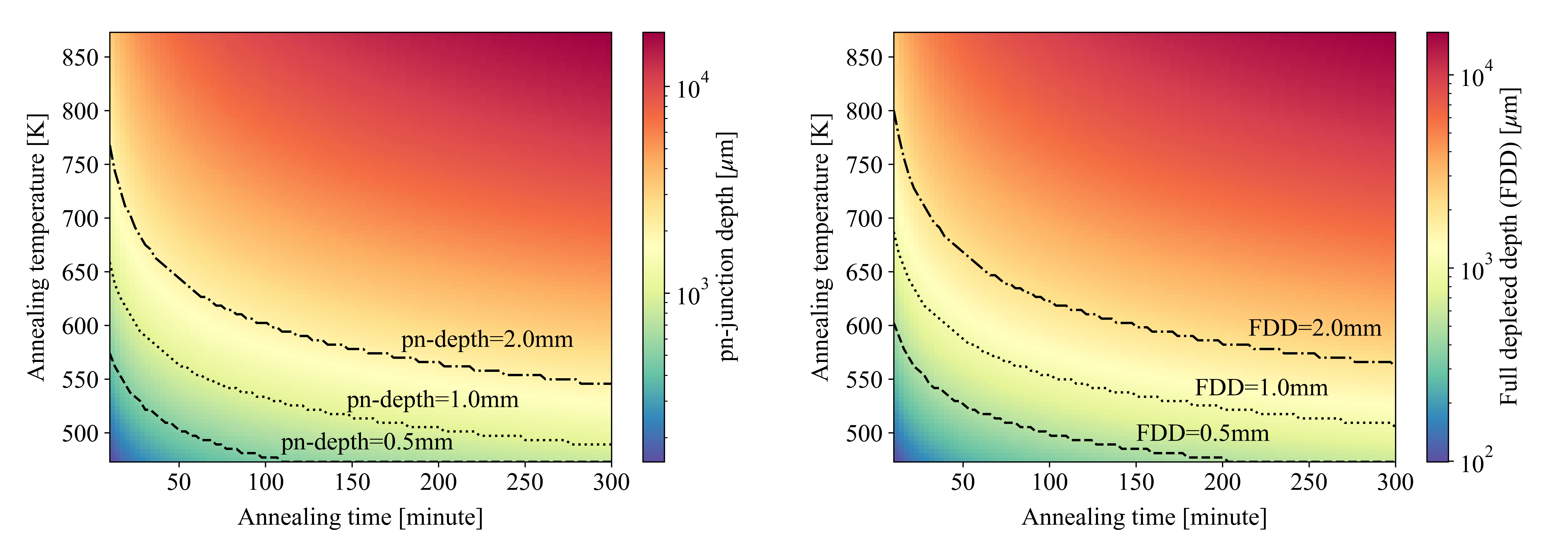
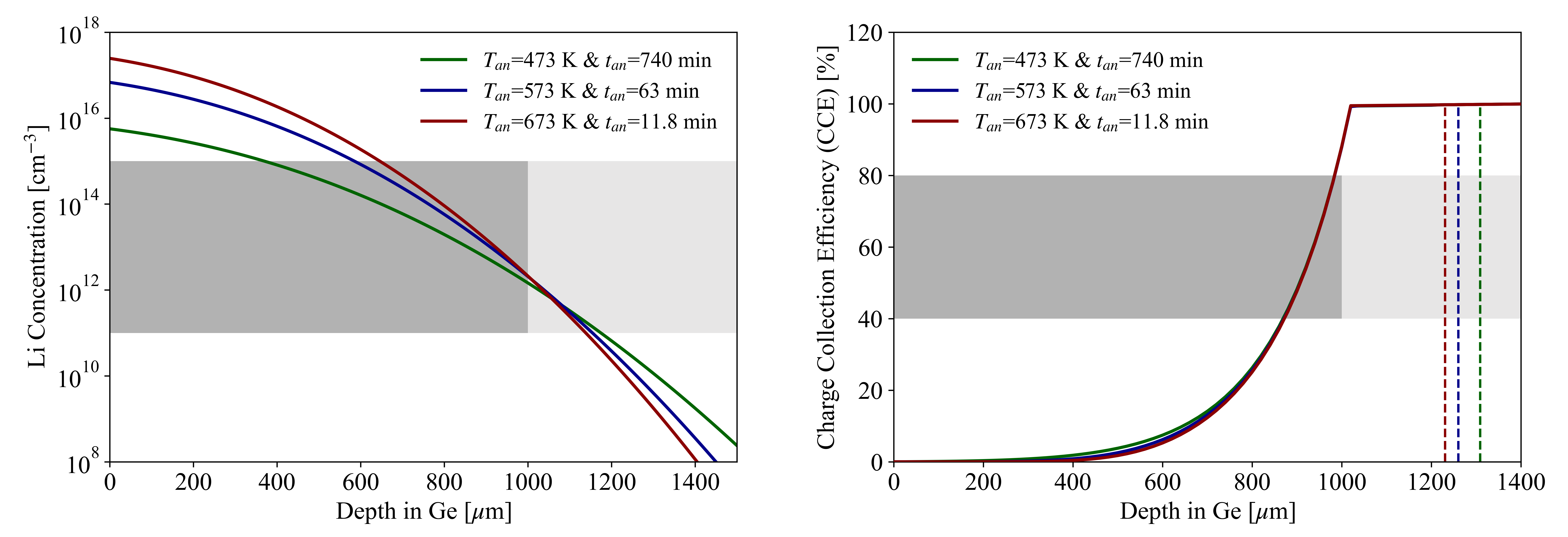
Different annealing processes could produce identical pn-junction depths or full depleted depths. However, the charge collection efficiencies and the full charge collections depth may differ due to the difference in Li concentration profiles in the N-type layer. Annealing processes with identical pn-junction depths (1 mm) and FDD (1 mm) are selected, and the corresponding CCEs are calculated assuming an electric field =1000 V/cm and a hole lifetime = 0.4 s. The results are shown in Fig.8 and Fig.9.
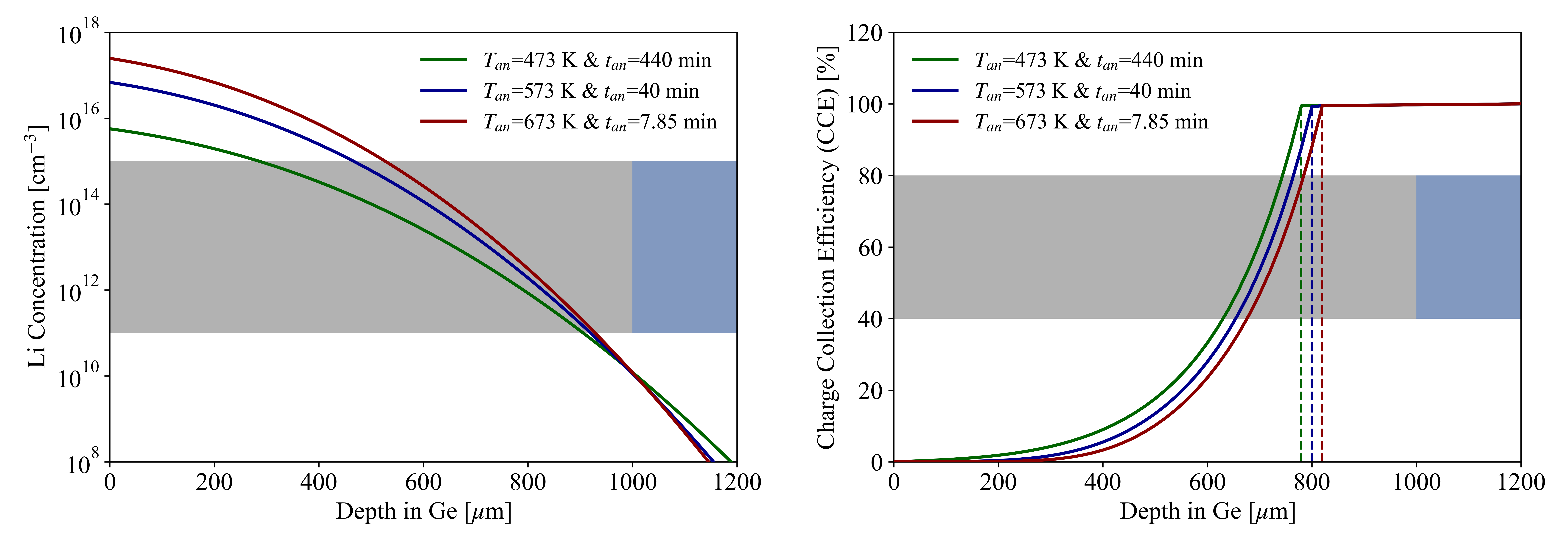
As shown in Fig.8, the thickness of the inactive layer (define as the full charge collection depth) and charge collection efficiencies vary from different annealing temperatures under the same pn-junction depth. A higher annealing temperature corresponds to lower charge collection efficiencies and a thicker inactive layer due to a thinner full depleted region and lower charge carrier mobilities in the N-type region.
As shown in Fig.9, different annealing processes with similar full depleted depths have presented approximative full charge collection depths and CCE profiles. Due to the steep profile of the electric fields (as shown in Fig.3) facilitating the collections of holes in the full depleted region, the CCE quickly reaches 100% in the full depleted region. It shows that the full depleted depth is a better parameter to describe the thickness of the inactive layer compared to the depth of the pn-junction.
4 Conclusions
A 1-D model describes the charge collections in the Li-diffused inactive layer of the P-type HPGe detector has been developed in this work. The charge collection efficiencies in different depths of the inactive layer can be calculated by solving the hole transportation equation. The effects of Li doping process, the annealing temperature, and the annealing time on the charge collection efficiency are evaluated. And the assessment shows the structure of inactive layer varies according to the Li-diffusion process and the thickness of the inactive layer mainly depends on the full depleted depth rather than the position of the pn-junction.
The charge collection efficiencies of the CDEX-1B (PPCGe) detector is calculated using the inactive layer model. The model is validated in another P-type semi-planar Ge detector. The full charge collection depth and charge collection efficiencies in different depths for both detectors agree with measurements.
The implementation of this model requires some detector specified parameters, e.g., the annealing time and temperature of the Li-diffusion process, recording those parameters during the fabrication can help to build a more precise model of the inactive layer. The hole lifetime in the inactive layer is a fairly complicated matter, we take a simple constant assumption in this work for lack of detail knowledge on the recombination and trapping processes. An average hole lifetime () in the inactive layer can be estimated by scanning to match the simulated spectra with measurements.
The model in this work can be easily extended to other types of P-type Ge detector (ICPC, BEGe, Coaxial) by adjusting the detector specified parameters in the model.
Acknowledgments:
This work was supported by the National Key Research and Development Program of China (Grant No. 2017YFA0402200) and the National Natural Science Foundation of China (Grant No. 12175112, No. 12005111, and No. 11725522).
References
- [1] R. D. Baertsch and N. R. Hall. IEEE Trans Nucl Sci. 17, 3, 235-240, (1970).
- [2] W. L. Hansen. Nucl. Instrum. Methods. 94, 377-380 (1971).
- [3] E.E. Haller. Mater Sci Semicond Process. 9, 4, 408-422 (2006).
- [4] L. T. Yang, et al. Chinese Phys. C. 42, 023002 (2018).
- [5] H. Jiang, et al. Phys. Rev. Lett. 120, 241301 (2018).
- [6] A. K. soma, et al. Nucl. Instrum. Methods. Phys. Res. A. 836, 67 (2016).
- [7] N. Abgrall, et al. (Majorana Collaboration), Phys. Rev. Lett. 118, 161801 (2017).
- [8] M. Agostini, et al. (GERDA Collaboration), Phys. Rev. Lett. 125, 011801 (2020).
- [9] M. Agostini, et al. (GERDA Collaboration), Phys. Rev. Lett. 125, 252502 (2020).
- [10] S. I. Alvis, et al. (Majorana Collaboration), Phys. Rev. C 100, 025501 (2019).
- [11] E. Aguayo, et al. Nucl. Instrum. Methods A. 701, 176–185 (2013).
- [12] H. Jiang, et al. Chinese Phys. C. 40, 096001 (2016).
- [13] L.T. Yang, et al. Nucl. Instrum. Methods A. 886, 13-23 (2018).
- [14] H.B. Li, et al. Astropart. Phys. 56, 1-8 (2014).
- [15] B. Lehnert. Journal of Physics: Conference Series 718, 062035 (2016).
- [16] J.L. Ma, et al. Appl Radiat Isot. 127, 130-136 (2017).
- [17] W. Shockley. J. Appl. Phys. 9, 635 (1938).
- [18] S. Ramo. Proceedings of the I.R.E. 584, (1939).
- [19] R.J. Cooper, et al. Nucl. Instrum. Methods A, 629, 1 (2011).
- [20] B. Pratt and F. Friedman. J. Appl. Phys. 37, 1893 (1966).
- [21] Q. Looker. PhD Thesis,University of California, (2014).
- [22] B. Lehnert. PhD Thesis, Dresden University of Technology, (2016).
- [23] C. S. Fuller and J. A. Ditzenberger. Phys. Rev. 91, 193 (1953).
- [24] C. S. Fuller and J. C. Severiens. Phys. Rev. 96, 21 (1954).
- [25] G. H. R. Kegel, et al. J. Electrochem. Soc, 118, 10, 1662-1665 (1971).
- [26] H. Mei, et al. JINST, 11, P12021 (2016).
- [27] D. Chattopadhyay and H. J. Queisser. Rev. Mod. Phys. 53, 745 (1981).
- [28] N. Sclar. Phys. Rev. 104, 1559 (1956).
- [29] J. Bardeen and W. Shockley. Phys. Rev. 80, 72 (1950).
- [30] S. Wagner, et al. IEEE, 1160–1993 (1993).
- [31] J. Lauwaert and P. Clauws. Thin Solid Films, 518, 9, 2330-2333 (2010).
- [32] W. L. Hansen and E. E. Haller. IEEE Trans Nucl Sci, 28, 1, 541-543 (1981).
- [33] R. Pehl, et al. IEEE Trans Nucl Sci, 19, 265-269 (1972).
- [34] R.M.J. Li, et al. NUCL SCI TECH 33, 57 (2022).
- [35] Z. She, et al. J. Instrum. 16, T09005 (2021).
- [36] S. Agostinelli, et al. Nucl. Instrum. Methods A, 3, 506, 250-303 (2003).