Further author information: (Send correspondence to Jack Lashner)
Jack Lashner: E-mail: lashner@usc.edu
The Simons Observatory: Complex Impedance Measurements for a Full Focal-Plane Module
Abstract
The Simons Observatory (SO) is a ground based Cosmic Microwave Background experiment that will be deployed to the Atacama Desert in Chile. SO will field over 60,000 transition edge sensor (TES) bolometers that will observe in six spectral bands between 27 GHz and 280 GHz with the goal of revealing new information about the origin and evolution of the universe. SO detectors are grouped based on their observing frequency and packaged into Universal Focal Plane Modules, each containing up to 1720 detectors which are read out using microwave SQUID multiplexing and the SLAC Microresonator Radio Frequency Electronics (SMuRF). By measuring the complex impedance of a TES we are able to access many thermoelectric properties of the detector that are difficult to determine using other calibration methods, however it has been difficult historically to measure complex impedance for many detectors at once due to high sample rate requirements. Here we present a method which uses SMuRF to measure the complex impedance of hundreds of detectors simultaneously on hour-long timescales. We compare the measured effective thermal time constants to those estimated independently with bias steps. This new method opens up the possibility for using this characterization tool both in labs and at the site to better understand the full population of SO detectors.
1 Introduction
The Simons Observatory (SO) is a new Cosmic Microwave Background (CMB) experiment being built on Cerro Toco in Chile, which will make precision measurements of the temperature and polarization anisotropies of the CMB in order to measure and constrain fundamental properties of the Universe [1]. SO will field over 60,000 Transition Edge Sensor (TES) detectors, split between a 6 m crossed Dragone large aperture telescope (LAT)[2, 3] containing 30,000+ detectors, and an array of three 42 cm small aperture refracting telescopes (SATs) containing a total of 30,000 detectors [4, 2, 5]. SO will use dichroic pixels observing in six spectral bands, at frequencies 27/39 GHz (LF), 93/145 GHz (MF) and 225/280 GHz (UHF) in order to measure the CMB and remove foreground contamination.
Advancements in readout architecture are essential to accommodate the large detector counts of SO and future CMB experiments. High multiplexing factors are necessary to decrease the thermal loading on the focal-plane, and decrease the complexity of the readout wiring. SO will use microwave superconducting quantum interference device (SQUID) multiplexing (mux) [6], where TESs are inductively coupled to superconducting microresonators between 4-6 GHz via RF SQUIDs. The SQUID coupling transduces current through the TES into a change in effective inductance of the microresonator, causing a measurable shift in its resonance frequency. At room temperature we use SLAC Microwave RF (SMuRF) electronics [7] to generate the tones used to interrogate resonators and track their resonance frequencies. In addition, SMuRF provides DC TES bias voltages, and the flux-ramp signal which is used to linearize the RF SQUID response.
The optical coupling, detector arrays, and cold electronics are all packaged together into 150 mm hexagonal assemblies called universal focal-plane modules (UFM) [8]. The focal planes of each telescope will be composed of tiled UFMs, with each SAT focal-plane containing 7 modules, and each of seven LAT optics tubes containing 3 modules. UFMs can support up to 1820 multiplexing channels and up to 1728 optical detectors, and will be read out using two Radio Frequency (RF) transmission lines. The UFM also provides routing for the 12 DC bias lines used to bias to the TESs, and two flux ramp lines used to linearize the SQUID response [9].
Before deployment, each UFM is tested and characterized in an SO testbed [10]. By measuring detector noise, current-voltage curves (IVs), and measuring the change in current through the TES in response to a small step in DC bias voltage (bias steps), we are able to determine detector properties such as the normal TES resistance (), the bias power required to drive detectors to 90% of (), the thermal conductance , and the effective thermal time constant . Some detector parameters such as the logarithmic sensitivities to temperature and current ( and respectively), the loop-gain , and the TES heat capacity are difficult to measure independently from each other due to degeneracy. The complex impedance (CI) of the TES provides a method by which we can access these parameters by measuring the response of the TES to sinusoidal bias voltage stimuli. CI measurements have previously been performed on SO prototype bolometers [11], however these measurements have been limited to only a few bolometers due to the high sample rate requirements. The high bandwidth of SMuRF allows us to take data at sample rates of up to 25 kHz for over 150 detectors at a time, and the Digital to Analog Converters (DACs) that power the bias lines can be used to send sine waves along the TES bias lines at frequencies approaching 5 kHz. SMuRF allows us to measure the complex impedance of large batches of TESs simultaneously, and perform preliminary and in-situ array-scale characterization in a matter of hours.
In this paper, we describe a procedure of measuring the complex impedance of SO detectors at array scales using the SMuRF readout electronics. Section 2 presents the TES model used to interpret the CI measurements. Section 3 describes the methods used to characterize detectors with complex impedance measurements, and bias step measurements. Section 4 presents the complex impedance results for a prototype UFM, and compares the effective thermal time constants with those calculated based on bias steps.
2 Background
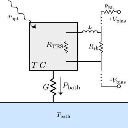
To model the complex impedance of the TES, we follow the formalism used by Irwin and Hilton [12] and model the TES bolometer as a single thermal block with temperature and heat capacity . This is a very simplified model, but measuring the complex impedance of the TES can help us understand departures from these assumptions. The TES is coupled to a thermal bath of temperature with thermal conductance . We bias the detectors using a constant-voltage bias that is applied to each bias line, which consists of a large bias line resistor in series with around 150 TES circuits. Each TES circuit is modeled as the TES resistance in series with a parasitic inductance , and with a shunt resistor m connected in parallel. A depiction of this model can be seen in Figure 1.
We substitute the full bias schematic shown in Figure 1 with a Thevenin equivalent circuit containing just a single TES, with equivalent voltage and equivalent impedance where both are complex phasors that depend on the excitation frequency . For the bias circuit described above, the equivalent impedance at low frequencies is given by . The dynamics of the TES are governed by the set of coupled differential equations:
| (1) |
| (2) |
where is the power flowing from the TES to the thermal bath, the power from joule heating, the power deposited onto the TES through optical coupling, and the TES resistance.
Under the constant-voltage bias, in-transition detectors are able to achieve negative electrothermal feedback which keeps the TES in transition. The detector is characterized by its logarithmic temperature sensitivity, logarithmic current sensitivity, and the loop-gain:
| (3) |
where , , and are the equilibrium current, bolometer temperature and bias power.
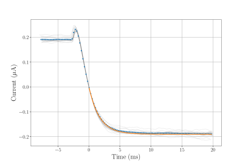
For small perturbations and , equations 1 and 2 can be linearized and solved[13]. These solutions contain two time constants: characterizing the initial electrical response, and characterizing the effective thermal decay to equilibrium. Both time constants can be seen in a TES’s response to a sudden voltage bias step, as is shown in Figure 5. SO bolometers have a very small inline inductance , which causes to be much longer than and makes the determining factor for how fast the TES can respond to an optical signal.
Solving the coupled differential equation yields
| (4) |
where is the natural thermal time constant in the absence of electrothermal feedback and is the thermal time constant in the case of a constant-current bias source.
The complex impedance of the TES can be extracted from the general solutions, and is given by
| (5) |
where is the excitation frequency. can be accessed by measuring the transfer function across the TES as is described in the next section.
3 Methods
The measurements in this section were carried out on a prototype SO UFM in a testbed designed for optical characterization of SO detectors [14]. Two thirds of the detectors in the UFM are covered by a gold-plated silicon mask allowing us to test both optical and dark detectors simultaneously. IVs taken immediately prior are used to determine parameters such as . The DC voltages for each TES bias line were chosen based on IVs to maximize the number of detectors with resistances in the range 30% - 60% . Note that the measurements shown in this section demonstrate a useful characterization method, but do not reflect expected operating parameters. The measurements were taken at a higher bath temperature (150 mK) than that expected during site observation (100 mK), and this particular set of TESs have optical efficiency that is too low to be deployed for observations.
3.1 Complex Impedance Measurement
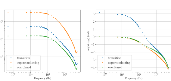
The transfer function of the TES in response to an excitation frequency is measured by sending a small sine wave along the bias line on top of the DC bias voltage biasing the TESs into transition. For each data sample, the commanded output of the DACs driving the TES bias line is recorded along with the TES response. We use these commanded TES bias values as a reference for a digital lock-in procedure[15] that allows us to extract the amplitude and phase of the TES response relative to the commanded bias with high levels of signal-to-noise. We measure the transfer function while the detectors are superconducting, overbiased, and in transition which can be seen in Figure 2. The superconducting and overbiased measurements allow us to estimate the Thevenin equivalent voltage and impedance of the system for every TES bias circuit at each frequency [16] and thus correct for stray impedances in the system. and are given by
| (6) |
| (7) |
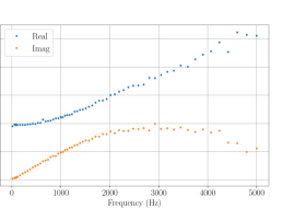
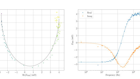
and the measured values for a single detector can be seen in Figure 3.
The complex impedance of the TES is then given by
| (8) |
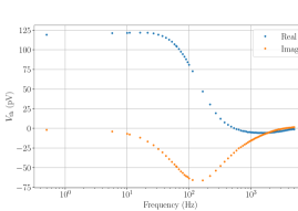
where is the complex phasor representing the TES current in transition. for a single detector can be seen in Figure 4. The measured for each detector is then fit using the model in equation 5 for the parameters , , and , which are used to compute derived parameters such as and .
Bipolar sine waves between 1 Hz and 5 kHz are applied to each bias line on top of the DC TES bias voltage, with an amplitude of around 0.1% of the DC bias level. The frequencies of the sine waves are limited by how quickly the two DACs that generate the TES bias voltages can be programmed. With the default SMuRF 1 MHz clock-rate, the bias voltage can be updated at around 16 kHz. This update rate can be increased by either increasing the clock-rate, or by only sending a sine wave on a single DAC while keeping the other fixed. As we approach excitation frequencies of 5 kHz the DACs can only be updated a few times per cycle, however using digital lock-in procedure we are still able to extract amplitudes and phases from the TES response. There is a small amount variation in the amplitude of the output sine wave at higher frequencies as can be seen in Figure 2, however, as shown in Figure 3 this is absorbed into and does not effect the measurement. approaches negative at low frequencies and at high frequencies, so high fidelity measurements out to high frequencies are particularly important for constraining . We sample detectors at 25 kHz, well above the Nyquist rate of the 5 kHz excitation.
Performing this measurement on a full UFM takes around 30 minutes, with the measurement time being limited by the fact that we need to measure the TES response in 12 batches, corresponding to the 12 bias lines on our UFM. The measurement is bottlenecked by the low-frequency data points, which require more time due to their longer periods. The measurement time can be shortened by reducing the number of samples at low excitation frequencies, and by reducing the number of periods we measure for those particular samples. It is sufficient to take superconducting and overbiased measurements once per array, and those measurements can be used for all in-transition measurements. This can be run in parallel across multiple UFMs simultaneously, resulting in an estimated measurement time for 30,000 detectors of approximately 2 hours.
Due to performance issues in the cryostat used to take these measurements, it was not possible to heat the array to perform tests at multiple bath temperatures. This causes certain parameters such as and to be poorly constrained, and could cause degeneracy between parameters such as and . One could improve these measurements by taking data at multiple bath temperatures and bias levels, forcing to remain constant across datasets.
3.2 Bias Step Measurement
We compare the measured using complex impedance to those independently measured from bias steps taken immediately before. Bias step measurements consist of biasing the detectors into their transition, and then sending a small-amplitude square wave on top of the DC bias voltage [17, 11]. We perform many steps in quick succession, and align each step such that it crosses the midpoint at . We then use the aligned steps to compute the mean response for each TES. We fit the thermal decay of the mean step response with a single-pole exponential of the form . We only fit the response after to avoid the initial electrical response of the TES. In Figure 5 we show each of the steps after alignment, the mean step, and the exponential fit for a single TES.
To command the bias steps, we use SMuRF’s arbitrary waveform generator to play a square wave with a period of 50 ms, and amplitude of around 1% of the DC bias voltage. We take data on one bias line at a time to avoid crosstalk between bias lines, and sample detectors at 4 kHz. We apply around 40 individual steps to improve the statistical significance of our measurements. This measurement takes around 30 seconds for a full UFM, making it a very useful tool for characterizing detectors throughout an observation.
4 Results
We performed the measurements described in Section 3 on an early prototype UFM, and obtained data for 663 TESs. This population includes both 90 and 150 GHz detectors, and includes both detectors that are blocked off at the UFM, and those that have an optical pathway out to room temperature. This is a relatively low yield for a full UFM, partially due to the elevated bath temperatures causing most of the optical 90 GHz detectors to be saturated, but it is enough to observe population statistics and trends. Figure 6 shows a comparison between and for each channel that passed data quality cuts. In general we see good agreement between the two datasets, though bias step calculations slightly overestimate compared to the complex impedance estimation, with this bias being worse for faster detectors. It is possible that this bias stems from inadequacies of using a single-pole exponential to fit the bias data, as it has been seen that the fitted is somewhat sensitive to our choice of [18].
Figure 7 shows all CI fit parameters for each channel, and how they compare to one another. From these fits, it is clear that the loop-gain , and thus the derived parameter , are poorly constrained by this dataset. For optimally biased detectors, we expect large values of , at least greater than 10. In this regime the loop-gain has a negligible effect on the complex impedance in equation 5 compared to and , and so fits tend to gravitate towards the limit.
A better estimation of could be achieved by repeating this measurement at various bath temperatures, fixing across the datasets. Alternatively, one could fix the thermal coupling coefficient to values measured by taking IVs at various temperatures [10].


5 Conclusion
In this work we present complex impedance results for 663 TESs on a prototype UFM. We compare the effective thermal time constant , determined from the complex impedance measurement, with those estimated using bias-steps. We observe that, though there is general agreement between the two methods, bias-steps slightly overestimate relative to complex impedance measurements. We also observe that certain parameters such as are not well constrained by these complex impedance measurements. This is unsurprising because we were operating at high bath temperatures due to performance issues of our cryostat.
This work demonstrates a new implementation for characterizing TESs enabled by advances in readout technology that allows us to take in-situ complex impedance measurements of thousands of detectors using SMuRF electronics. This allows us to study population statistics for detector parameters that have been historically difficult to measure, which can inform future detector design. Because this method does not require specialized hardware, it can be run at the site to monitor parameters so they can be accessed by the SO analysis pipeline for improved mapping. In the future we plan on optimizing this measurement so it takes less time, and retaking this data for SO deployment UFMs at operational temperatures to better constrain these parameters, and to explore how SO bolometers deviate from the simple thermal model presented here.
6 Acknowledgements
This work was supported in part by a grant from the Simons Foundation (Award #457687, B.K.).
References
- [1] Ade, P., Aguirre, J., Ahmed, Z., Aiola, S., Ali, A., Alonso, D., Alvarez, M. A., Arnold, K., Ashton, P., Austermann, J., Awan, H., Baccigalupi, C., Baildon, T., Barron, D., Battaglia, N., Battye, R., Baxter, E., Bazarko, A., Beall, J. A., Bean, R., Beck, D., Beckman, S., Beringue, B., Bianchini, F., Boada, S., Boettger, D., Bond, J. R., Borrill, J., Brown, M. L., Bruno, S. M., Bryan, S., Calabrese, E., Calafut, V., Calisse, P., Carron, J., Challinor, A., Chesmore, G., Chinone, Y., Chluba, J., Cho, H.-M. S., Choi, S., Coppi, G., Cothard, N. F., Coughlin, K., Crichton, D., Crowley, K. D., Crowley, K. T., Cukierman, A., D’Ewart, J. M., Dünner, R., de Haan, T., Devlin, M., Dicker, S., Didier, J., Dobbs, M., Dober, B., Duell, C. J., Duff, S., Duivenvoorden, A., Dunkley, J., Dusatko, J., Errard, J., Fabbian, G., Feeney, S., Ferraro, S., Fluxà, P., Freese, K., Frisch, J. C., Frolov, A., Fuller, G., Fuzia, B., Galitzki, N., Gallardo, P. A., Ghersi, J. T. G., Gao, J., Gawiser, E., Gerbino, M., Gluscevic, V., Goeckner-Wald, N., Golec, J., Gordon, S., Gralla, M., Green, D., Grigorian, A., Groh, J., Groppi, C., Guan, Y., Gudmundsson, J. E., Han, D., Hargrave, P., Hasegawa, M., Hasselfield, M., Hattori, M., Haynes, V., Hazumi, M., He, Y., Healy, E., Henderson, S. W., Hervias-Caimapo, C., Hill, C. A., Hill, J. C., Hilton, G., Hilton, M., Hincks, A. D., Hinshaw, G., Hložek, R., Ho, S., Ho, S.-P. P., Howe, L., Huang, Z., Hubmayr, J., Huffenberger, K., Hughes, J. P., Ijjas, A., Ikape, M., Irwin, K., Jaffe, A. H., Jain, B., Jeong, O., Kaneko, D., Karpel, E. D., Katayama, N., Keating, B., Kernasovskiy, S. S., Keskitalo, R., Kisner, T., Kiuchi, K., Klein, J., Knowles, K., Koopman, B., Kosowsky, A., Krachmalnicoff, N., Kuenstner, S. E., Kuo, C.-L., Kusaka, A., Lashner, J., Lee, A., Lee, E., Leon, D., Leung, J. S.-Y., Lewis, A., Li, Y., Li, Z., Limon, M., Linder, E., Lopez-Caraballo, C., Louis, T., Lowry, L., Lungu, M., Madhavacheril, M., Mak, D., Maldonado, F., Mani, H., Mates, B., Matsuda, F., Maurin, L., Mauskopf, P., May, A., McCallum, N., McKenney, C., McMahon, J., Meerburg, P. D., Meyers, J., Miller, A., Mirmelstein, M., Moodley, K., Munchmeyer, M., Munson, C., Naess, S., Nati, F., Navaroli, M., Newburgh, L., Nguyen, H. N., Niemack, M., Nishino, H., Orlowski-Scherer, J., Page, L., Partridge, B., Peloton, J., Perrotta, F., Piccirillo, L., Pisano, G., Poletti, D., Puddu, R., Puglisi, G., Raum, C., Reichardt, C. L., Remazeilles, M., Rephaeli, Y., Riechers, D., Rojas, F., Roy, A., Sadeh, S., Sakurai, Y., Salatino, M., Rao, M. S., Schaan, E., Schmittfull, M., Sehgal, N., Seibert, J., Seljak, U., Sherwin, B., Shimon, M., Sierra, C., Sievers, J., Sikhosana, P., Silva-Feaver, M., Simon, S. M., Sinclair, A., Siritanasak, P., Smith, K., Smith, S. R., Spergel, D., Staggs, S. T., Stein, G., Stevens, J. R., Stompor, R., Suzuki, A., Tajima, O., Takakura, S., Teply, G., Thomas, D. B., Thorne, B., Thornton, R., Trac, H., Tsai, C., Tucker, C., Ullom, J., Vagnozzi, S., van Engelen, A., Lanen, J. V., Winkle, D. D. V., Vavagiakis, E. M., Vergès, C., Vissers, M., Wagoner, K., Walker, S., Ward, J., Westbrook, B., Whitehorn, N., Williams, J., Williams, J., Wollack, E. J., Xu, Z., Yu, B., Yu, C., Zago, F., Zhang, H., and and, N. Z., “The Simons Observatory: Science goals and forecasts,” Journal of Cosmology and Astroparticle Physics 2019, 056–056 (Feb. 2019).
- [2] Zhu, N., Bhandarkar, T., Coppi, G., Kofman, A. M., Orlowski-Scherer, J. L., Xu, Z., Adachi, S., Ade, P., Aiola, S., Austermann, J., Bazarko, A. O., Beall, J. A., Bhimani, S., Bond, J. R., Chesmore, G. E., Choi, S. K., Connors, J., Cothard, N. F., Devlin, M., Dicker, S., Dober, B., Duell, C. J., Duff, S. M., Dünner, R., Fabbian, G., Galitzki, N., Gallardo, P. A., Golec, J. E., Haridas, S. K., Harrington, K., Healy, E., Ho, S.-P. P., Huber, Z. B., Hubmayr, J., Iuliano, J., Johnson, B. R., Keating, B., Kiuchi, K., Koopman, B. J., Lashner, J., Lee, A. T., Li, Y., Limon, M., Link, M., Lucas, T. J., McCarrick, H., Moore, J., Nati, F., Newburgh, L. B., Niemack, M. D., Pierpaoli, E., Randall, M. J., Sarmiento, K. P., Saunders, L. J., Seibert, J., Sierra, C., Sonka, R., Spisak, J., Sutariya, S., Tajima, O., Teply, G. P., Thornton, R. J., Tsan, T., Tucker, C., Ullom, J., Vavagiakis, E. M., Vissers, M. R., Walker, S., Westbrook, B., Wollack, E. J., and Zannoni, M., “The Simons Observatory Large Aperture Telescope Receiver,” The Astrophysical Journal Supplement Series 256, 23 (Sept. 2021).
- [3] Parshley, S. C., Niemack, M., Hills, R., Dicker, S. R., Dünner, R., Erler, J., Gallardo, P. A., Gudmundsson, J. E., Herter, T., Koopman, B. J., Limon, M., Matsuda, F. T., Mauskopf, P., Riechers, D. A., Stacey, G. J., and Vavagiakis, E. M., “The optical design of the six-meter CCAT-prime and Simons Observatory telescopes,” in [Ground-Based and Airborne Telescopes VII ], 10700, 1292–1304, SPIE (July 2018).
- [4] Galitzki, N., Ali, A., Arnold, K. S., Ashton, P. C., Austermann, J. E., Baccigalupi, C., Baildon, T., Barron, D., Beall, J. A., Beckman, S., Bruno, S. M. M., Bryan, S., Calisse, P. G., Chesmore, G. E., Chinone, Y., Choi, S. K., Coppi, G., Crowley, K. D., Crowley, K. T., Cukierman, A., Devlin, M. J., Dicker, S., Dober, B., Duff, S. M., Dunkley, J., Fabbian, G., Gallardo, P. A., Gerbino, M., Goeckner-Wald, N., Golec, J. E., Gudmundsson, J. E., Healy, E. E., Henderson, S., Hill, C. A., Hilton, G. C., Ho, S.-P. P., Howe, L. A., Hubmayr, J., Jeong, O., Keating, B., Koopman, B. J., Kuichi, K., Kusaka, A., Lashner, J., Lee, A. T., Li, Y., Limon, M., Lungu, M., Matsuda, F., Mauskopf, P. D., May, A. J., McCallum, N., McMahon, J., Nati, F., Niemack, M. D., Orlowski-Scherer, J. L., Parshley, S. C., Piccirillo, L., Rao, M. S., Raum, C., Salatino, M., Seibert, J. S., Sierra, C., Silva-Feaver, M., Simon, S. M., Staggs, S. T., Stevens, J. R., Suzuki, A., Teply, G., Thornton, R., Tsai, C., Ullom, J. N., Vavagiakis, E. M., Vissers, M. R., Westbrook, B., Wollack, E. J., Xu, Z., and Zhu, N., “The Simons Observatory: Instrument Overview,” Millimeter, Submillimeter, and Far-Infrared Detectors and Instrumentation for Astronomy IX , 3 (July 2018).
- [5] Ali, A. M., Adachi, S., Arnold, K., Ashton, P., Bazarko, A., Chinone, Y., Coppi, G., Corbett, L., Crowley, K. D., Crowley, K. T., Devlin, M., Dicker, S., Duff, S., Ellis, C., Galitzki, N., Goeckner-Wald, N., Harrington, K., Healy, E., Hill, C. A., Ho, S.-P. P., Hubmayr, J., Keating, B., Kiuchi, K., Kusaka, A., Lee, A. T., Ludlam, M., Mangu, A., Matsuda, F., McCarrick, H., Nati, F., Niemack, M. D., Nishino, H., Orlowski-Scherer, J., Sathyanarayana Rao, M., Raum, C., Sakurai, Y., Salatino, M., Sasse, T., Seibert, J., Sierra, C., Silva-Feaver, M., Spisak, J., Simon, S. M., Staggs, S., Tajima, O., Teply, G., Tsan, T., Wollack, E., Westbrook, B., Xu, Z., Zannoni, M., and Zhu, N., “Small Aperture Telescopes for the Simons Observatory,” Journal of Low Temperature Physics 200, 461–471 (Sept. 2020).
- [6] Mates, J. a. B., Hilton, G. C., Irwin, K. D., Vale, L. R., and Lehnert, K. W., “Demonstration of a multiplexer of dissipationless superconducting quantum interference devices,” Applied Physics Letters 92, 023514 (Jan. 2008).
- [7] Henderson, S. W., Ahmed, Z., Austermann, J., Becker, D., Bennett, D. A., Brown, D., Chaudhuri, S., Cho, H.-M. S., D’Ewart, J. M., Dober, B., Duff, S. M., Dusatko, J. E., Fatigoni, S., Frisch, J. C., Gard, J. D., Halpern, M., Hilton, G. C., Hubmayr, J., Irwin, K. D., Karpel, E. D., Kernasovskiy, S. S., Kuenstner, S. E., Kuo, C.-L., Li, D., Mates, J. A. B., Reintsema, C. D., Smith, S. R., Ullom, J., Vale, L. R., Van Winkle, D. D., Vissers, M., and Yu, C., “Highly-multiplexed microwave SQUID readout using the SLAC Microresonator Radio Frequency (SMuRF) Electronics for Future CMB and Sub-millimeter Surveys,” Millimeter, Submillimeter, and Far-Infrared Detectors and Instrumentation for Astronomy IX , 43 (July 2018).
- [8] McCarrick, H., Healy, E., Ahmed, Z., Arnold, K., Atkins, Z., Austermann, J. E., Bhandarkar, T., Beall, J. A., Bruno, S. M., Choi, S. K., Connors, J., Cothard, N. F., Crowley, K. D., Dicker, S., Dober, B., Duell, C. J., Duff, S. M., Dutcher, D., Frisch, J. C., Galitzki, N., Gralla, M. B., Gudmundsson, J. E., Henderson, S. W., Hilton, G. C., Ho, S.-P. P., Huber, Z. B., Hubmayr, J., Iuliano, J., Johnson, B. R., Kofman, A. M., Kusaka, A., Lashner, J., Lee, A. T., Li, Y., Link, M. J., Lucas, T. J., Lungu, M., Mates, J. A. B., McMahon, J. J., Niemack, M. D., Orlowski-Scherer, J., Seibert, J., Silva-Feaver, M., Simon, S. M., Staggs, S., Suzuki, A., Terasaki, T., Thornton, R., Ullom, J. N., Vavagiakis, E. M., Vale, L. R., Lanen, J. V., Vissers, M. R., Wang, Y., Wollack, E. J., Xu, Z., Young, E., Yu, C., Zheng, K., and Zhu, N., “The Simons Observatory Microwave SQUID Multiplexing Detector Module Design,” The Astrophysical Journal 922, 38 (Nov. 2021).
- [9] Mates, J. A. B., Irwin, K. D., Vale, L. R., Hilton, G. C., Gao, J., and Lehnert, K. W., “Flux-Ramp Modulation for SQUID Multiplexing,” Journal of Low Temperature Physics 167, 707–712 (June 2012).
- [10] Wang, Y., Zheng, K., Atkins, Z., Austermann, J., Bhandarkar, T., Choi, S. K., Duff, S. M., Dutcher, D., Galitzki, N., Healy, E., Huber, Z. B., Hubmayr, J., Johnson, B. R., Lashner, J., Li, Y., McCarrick, H., Niemack, M. D., Seibert, J., Staggs, S. T., Vavagiakis, E., and Xu, Z., “Simons Observatory Focal-Plane Module: In-lab Testing and Characterization Program,” arXiv:2111.11301 [astro-ph, physics:physics] (Nov. 2021).
- [11] Cothard, N. F., Ali, A. M., Austermann, J. E., Choi, S. K., Crowley, K. T., Dober, B. J., Duell, C. J., Duff, S. M., Gallardo, P., Hilton, G. C., Ho, S.-P. P., Hubmayr, J., Link, M. J., Niemack, M. D., Sonka, R. F., Staggs, S. T., Vavagiakis, E. M., Wollack, E. J., and Xu, Z., “Comparing complex impedance and bias step measurements of Simons Observatory transition edge sensors,” in [Millimeter, Submillimeter, and Far-Infrared Detectors and Instrumentation for Astronomy X ], 11453, 302–311, SPIE (Dec. 2020).
- [12] Irwin, K. and Hilton, G., “Transition-Edge Sensors,” in [Cryogenic Particle Detection ], Enss, C., ed., Topics in Applied Physics, 63–150, Springer, Berlin, Heidelberg (2005).
- [13] Becker, D. T., SUBMILLIMETER VIDEO IMAGING WITH A SUPERCONDUCTING BOLOMETER ARRAY, PhD thesis.
- [14] Seibert, J., Ade, P., Ali, A. M., Arnold, K., Cothard, N. F., Galitzki, N., Harrington, K., Ho, S.-P. P., Keating, B., Lowry, L. N., Russell, M., Silva-Feaver, M., Siritanasak, P., Teply, G. P., Tucker, C., Vavagiakis, E. M., and Xu, Z., “Development of an optical detector testbed for the Simons Observatory,” in [Millimeter, Submillimeter, and Far-Infrared Detectors and Instrumentation for Astronomy X ], 11453, 114532C, International Society for Optics and Photonics (Dec. 2020).
- [15] Probst, P. A. and Collet, B., “Low-frequency digital lock-in amplifier,” Review of Scientific Instruments 56, 466–470 (Mar. 1985).
- [16] Lindeman, M. A., Barger, K. A., Brandl, D. E., Crowder, S. G., Rocks, L., and McCammon, D., “Complex impedance measurements of calorimeters and bolometers: Correction for stray impedances,” Review of Scientific Instruments 78, 043105 (Apr. 2007).
- [17] Koopman, B. J., Cothard, N. F., Choi, S. K., Crowley, K. T., Duff, S. M., Henderson, S. W., Ho, S. P., Hubmayr, J., Gallardo, P. A., Nati, F., Niemack, M. D., Simon, S. M., Staggs, S. T., Stevens, J. R., Vavagiakis, E. M., and Wollack, E. J., “Advanced ACTPol Low-Frequency Array: Readout and Characterization of Prototype 27 and 39 GHz Transition Edge Sensors,” Journal of Low Temperature Physics 193, 1103–1111 (Dec. 2018).
- [18] Niemack, M. D., Towards Dark Energy: Design, Development, and Preliminary Data from ACT, PhD thesis (Jan. 2008).