Quasiparticle spectroscopy, transport, and magnetic properties
of Nb films used in superconducting transmon qubits
Abstract
Niobium thin films on silicon substrate used in the fabrication of superconducting qubits have been characterized using scanning and transmission electron microscopy, electrical transport, magnetization, quasiparticle spectroscopy, and real-space real-time magneto-optical imaging. We study niobium films to provide an example of a comprehensive analytical set that may benefit superconducting circuits such as those used in quantum computers. The films show outstanding superconducting transition temperature of K and a fairly clean superconducting gap, along with superfluid density enhanced at intermediate temperatures. These observations are consistent with the recent theory of anisotropic strong-coupling superconductivity in Nb. However, the response to the magnetic field is complicated, exhibiting significantly irreversible behavior and insufficient heat conductance leading to thermo-magnetic instabilities. These may present an issue for further improvement of transmon quantum coherence. Possible mitigation strategies are discussed.
I Introduction
Superconducting qubits are promising candidates for implementing large-scale quantum computers [1, 2, 3]. The advancement in fabrication and design of superconducting qubits have demonstrated impressive gate fidelity of up to 99.5 % for two-qubit gates, which is the measure of the ability of a device to faithfully execute quantum algorithms [4]. However, large-scale devices will require fidelity well beyond 99.9 % [5]. It was shown that certain impurities and defects in qubit material tend to shorten the coherence time and lead to overall lower fidelity operations [6, 7, 8]. For example, microwave loss at cryogenic temperatures has been attributed to the resonant coupling to two-level systems (TLS) physically composed of the atomic defects [9, 7]. Therefore, achieving better fidelities requires improved quantum coherence and that necessiates a better understanding and control over the materials used to fabricate qubits.
Niobium is the material of choice for various superconducting applications due to its relatively high transition temperature, K. Niobium thin films (100-200 nm thick) are used in the superconducting transmon qubits [1]. The “heart” of such qubits is an aluminum Josephson junction used to provide non-linearity to the circuit and niobium is used to fabricate the vast majority of the rest of the circuit: the readout resonators, capacitor pads, and coupling lines in the transmon. The structure must have a high degree of quantum coherence in all parts to work. Surfaces and interfaces are known to introduce noise and loss that play a major role in decreasing the coherence time in transmon qubits [10, 11, 12, 13, 7]. For instance, the presence of native amorphous oxides with different stoichiometry (NbO, NbO2 and Nb2O5) are believed to be the host for TLSs, hence decoherence [14, 15, 16, 17]. Another recently discovered source of potential decoherence in transmons is nano-sized niobium hydrides [7] (large hydrides in superconducting RF cavities are believed to be the cause of the so-called Q-disease (a dramatic reduction of the quality factor above some amplitude of electromagnetic field inside) and have been known for a long time [18, 19, 20, 21, 22, 23]). While bulk niobium used in SRF cavities was extensively characterized both in normal and the superconducting states, the niobium films used in QIS technologies have mostly been studied in the normal state and, in the superconducting state, specifically to examine the quality factor behavior and losses at GHz frequencies [24]. Bulk and film states of niobium are very different in terms of morphology, purity, and relative length scales involved, and more conventional studies in the superconducting state are needed.
In this work, we employ various techniques to study thermally excited quasiparticles, electrical transport, upper and third critical fields, magnetization and spatial distribution of the magnetic induction in niobium thin films and suggest the strategies for further optimizations and improvements.
II EXPERIMENTAL
Niobium films, 160 nm thick, were deposited onto [001] high-resistivity silicon wafers ( using high-power impulse magnetron sputtering (HiPIMS) in a ultra-high vacuum system with a base pressure Torr. [8].
The film morphology was studied using scanning and transmission electron microscopy, high-resolution SEM, and TEM. A more detailed investigation of the transmons from the same batch as in this work, and imaging details, are available elsewhere [25]. Cross-sectional and plan-view TEM samples were prepared with a Helios focused ion beam system. The TEM images were acquired at an acceleration voltage of 200 kV using a Titan Themis. The SEM was used to map out the larger view of sample surface morphology. The TEM images were used for quantitative analysis.
To study the low-energy quasiparticles, we used a tunnel-diode resonator for the precision measurements of the London penetration depth, [26, 27], which is then used to calculate the superfluid density, which is compared to the expectations from the theory.
Four-probe electrical resistivity measurements were performed in a Quantum Design PPMS. Contacts were made by gluing 25 silver wires using DuPont 4929N conducting silver paste. This technique yields contacts with contact resistance in the 10 to 100 range. Transport measurements of the upper critical field, , were performed with a magnetic field oriented perpendicular to the film plane to avoid the third critical field, , which does not exist in this orientation but is maximum when the magnetic field is parallel to the film surface [28, 29]. For measurements in a parallel configuration, the sample was glued on the side of the plastic cube, similar to those described in Ref. 30. This procedure provided alignment with the accuracy of about 2 degrees.
Total magnetization was measured using a vibrating sample magnetometer (VSM) module in Quantum Design PPMS. The advantage of this device is the ability to sweep the magnetic field continuously at a constant rate.
The two-dimensional distribution of the magnetic induction was mapped in real-time employing magneto-optical imaging using Faraday Effect (MOFA) in transparent ferrimagnetic indicators (bismuth-doped iron garnets) placed on top of the samples. The closed-cycle flow-type optical 4He cryostat exposed the cooled sample to an Olympus polarized-light microscope. The magnetic induction on the sample surface polarizes in-plane magnetic moments in the indicator, and the distribution of this polarization component along the light propagation is visualized through double Faraday rotation. In the images, only the magnetic field is visible due to a mirror sputtered at the bottom of the indicator [31, 32, 33, 34].
III Results
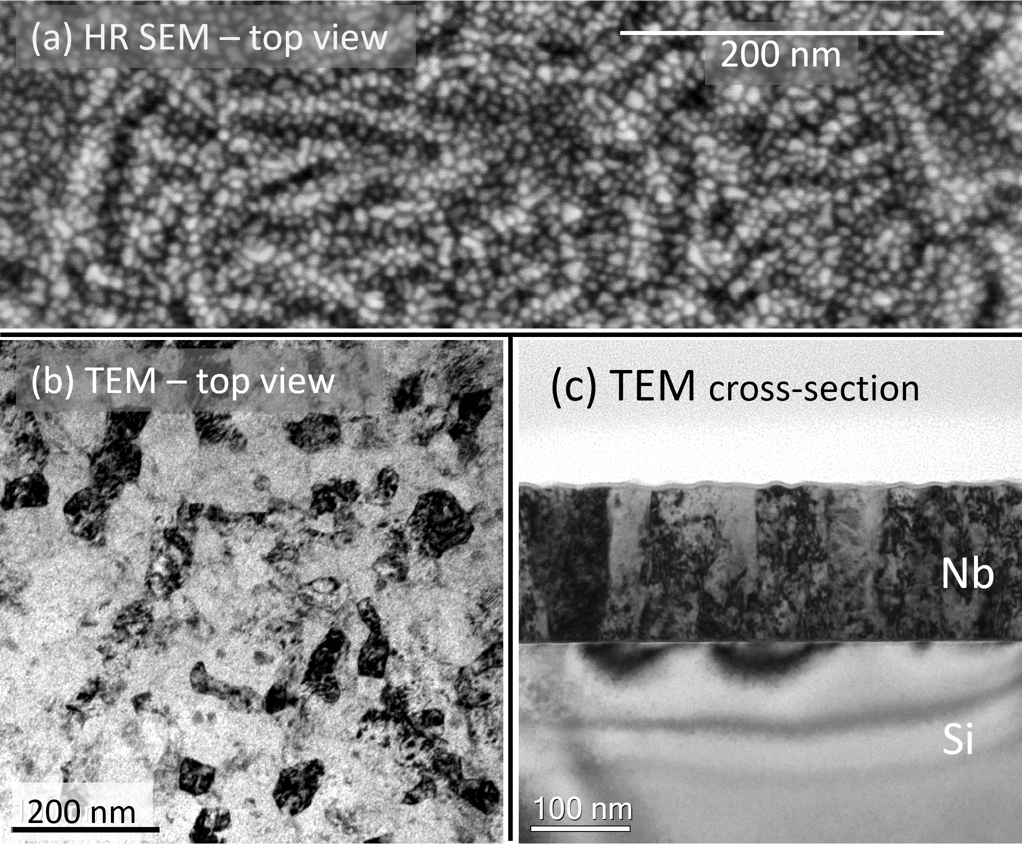
Figure 1 shows the morphology of the Nb film revealed by high-resolution scanning (HR-SEM) and transmission (TEM) electron microscopy. Figure 1(a) shows the SEM image of a wide view of the top surface morphology, revealing substantial spatial modulations at two characteristic length scales. Further details of internal and surface structural texture are revealed by bright-field plan-view TEM image, Fig.1(b), and cross-sectional view, Fig.1(c). The contrast variation reveals granular polycrystalline structure on top and inside the film with grain sizes ranging from 25 nm to 75 nm, with an average size of about 50 nm. Those grains have a columnar structure along film thickness, measured at 160 nm as intended by the fabrication. The smaller droplets observed in secondary electrons contrast, Fig.1(a), represent surface roughness also seen in the cross-sectional view, Fig.1(c).
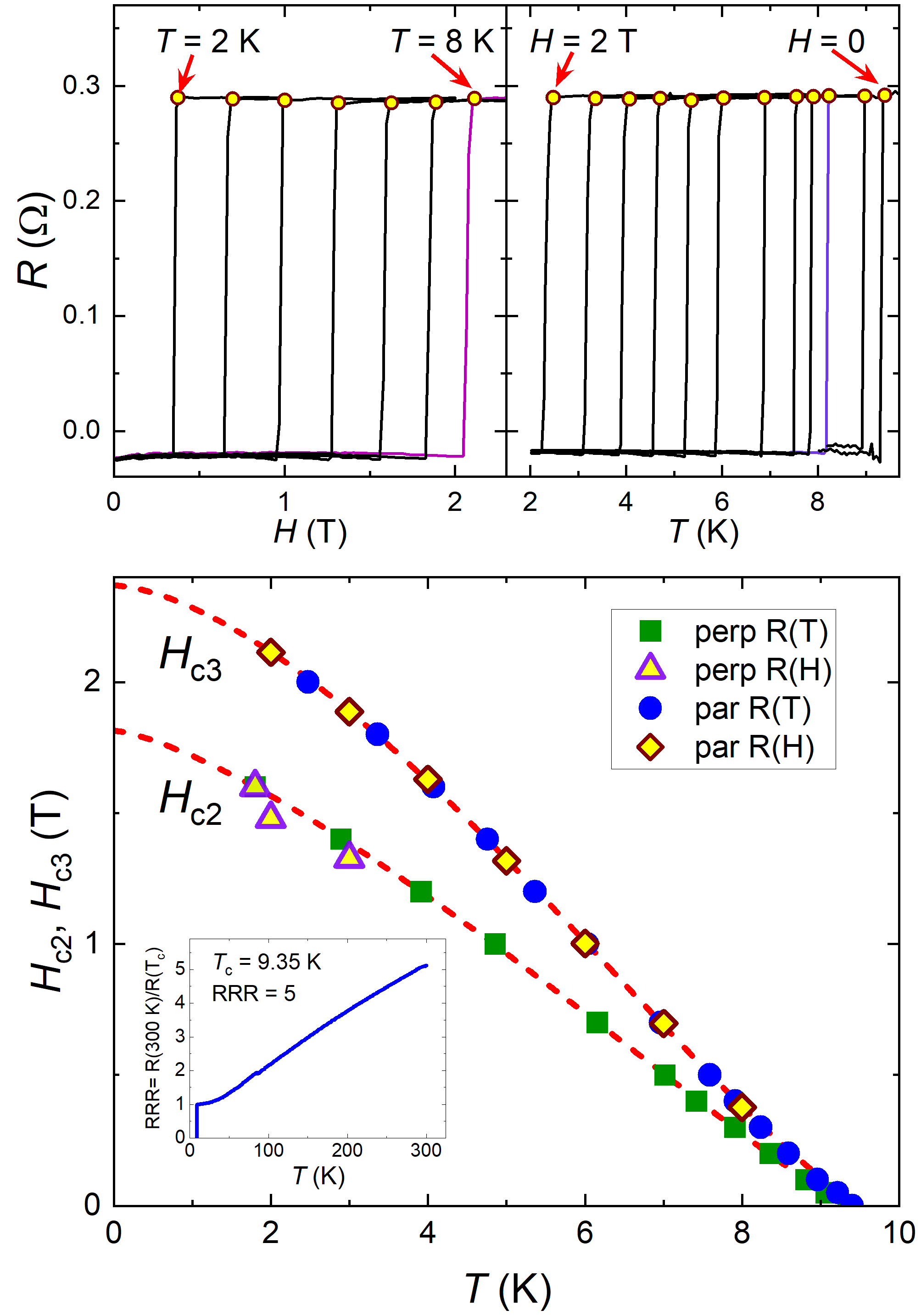
Figure 2 presents electrical resistivity measurements as a function of magnetic field and temperature. The data were collected in parallel and perpendicular orientations of the film with respect to the applied magnetic field. In a parallel orientation, the material remains superconducting up to a so-called third critical magnetic field, , surviving in a thin surface later of the order of the superconducting coherence length, [28, 29, 35]. In niobium, nm, depending on its purity and degree of crystallinity [28, 36, 37, 38]. In the perpendicular orientation of the magnetic field to the film plane, the upper critical field, , is the highest magnetic field possible [28, 29, 39]. Therefore, we obtain these two critical magnetic fields from the measurements of the same sample, simply rotating it by 90 degrees without changing the contacts. In the PPMS, the cooling is achieved via the helium exchange gas when the sample is mounted on a puck, and so the orientation is not important for thermal equilibrium as long as the measurements are performed slowly. Indeed, we see the same K in zero magnetic field in both orientations.
The top left panel of Fig.2 shows the magnetic field - dependent resistance, , measured at different temperatures from 2 to 8 K in 1 K steps. The top right panel shows the temperature-dependent resistance, , measured at different magnetic fields, from right to left: 0, 0.1, 0.3, 0.4, 0.5, 0.7, 1.0, 1.2, 1.4, 1.6, 1.8, and 2 T. In both top panels, the symbols show the locations of the third critical field, (left panel), or critical temperatures, (right panel), an easy pick, considering how sharp the transitions remain for all curves. Similar measurements were performed in the perpendicular orientation, yielding the upper critical field, . The bottom panel of Fig.2 summarizes the results of the critical fields measurements. The upper curve, obtained from the data in the top panels, shows the third critical field, . The agreement between the two types of scans is outstanding. Similarly, the lower curve shows the upper critical field, .
The inset shows temperature-dependent resistivity normalized by its value at in a broad temperature range up to 300 K. At 300 K, this ratio, called the residual resistivity ratio, , is the commonly used measure of scattering on defects and impurities. For comparison, the cleanest niobium samples reach [40], and so the value of 5 for our films is rather low.
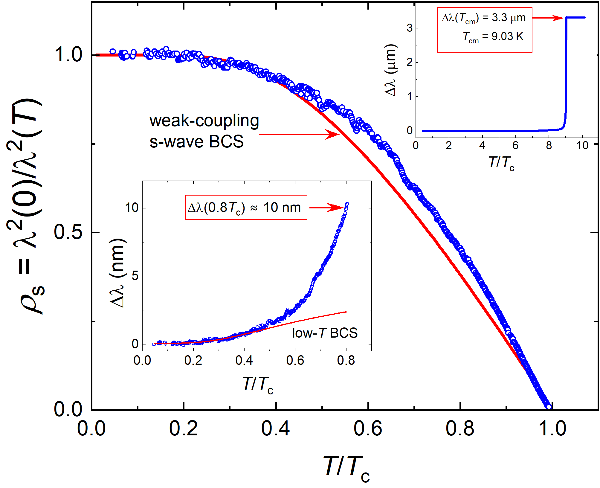
We now examine the superconducting state of the studied films. Figure 3 shows the temperature-dependent superfluid density, , obtained from the London penetration depth, , measured using tunnel-diode resonator [26, 27]. The solid red curve is the expectation from the isotropic weak-coupling Bardeen-Cooper-Schrieffer (BCS) theory [41]. This measurement is quite difficult due to the extreme thin-film geometry. The upper inset in Fig.3 shows the full transition curve, which looks flawless, but cuts off at about , at which point the film becomes transparent to our 10 MHz RF AC field. This formally follows from the analysis of the magnetic susceptibility in finite samples [42]. For our films, the formal calibration gives for the effective sample size, , which matches perfectly the above experimental value for the penetration depth at when the response becomes “sample size limited” [42]. This also explains why the measured K is a little lower than K detected by the transport measurements, Fig.2. The lower inset zooms into the lower temperature behavior. Remarkably, the penetration depth changes only by 10 nm from the base temperature up to . And yet we were able to resolve the whole superfluid density curve shown in the main panel of Fig.3. A clear exponential attenuation at low temperatures signals a full superconducting gap. If we fit the data to a low-temperature BCS formula, valid below , [27], where and and use as a free parameter, we obtain instead of isotropic BCS value of . This is most likely associated with the electronic and superconducting states anisotropy of niobium, and its multiband nature [38]. In this situation, the range of exponential attenuation is determined by the smaller gap, specifically on band 2, which also dominates the thermodynamic response [38]. The theory is further confirmed by the observed deviation of the experimental superfluid density at elevated temperatures from the weak coupling expectation, shown by the solid red line in the main panel of Fig.3. Stronger coupling makes lie above the weak coupling values [38].
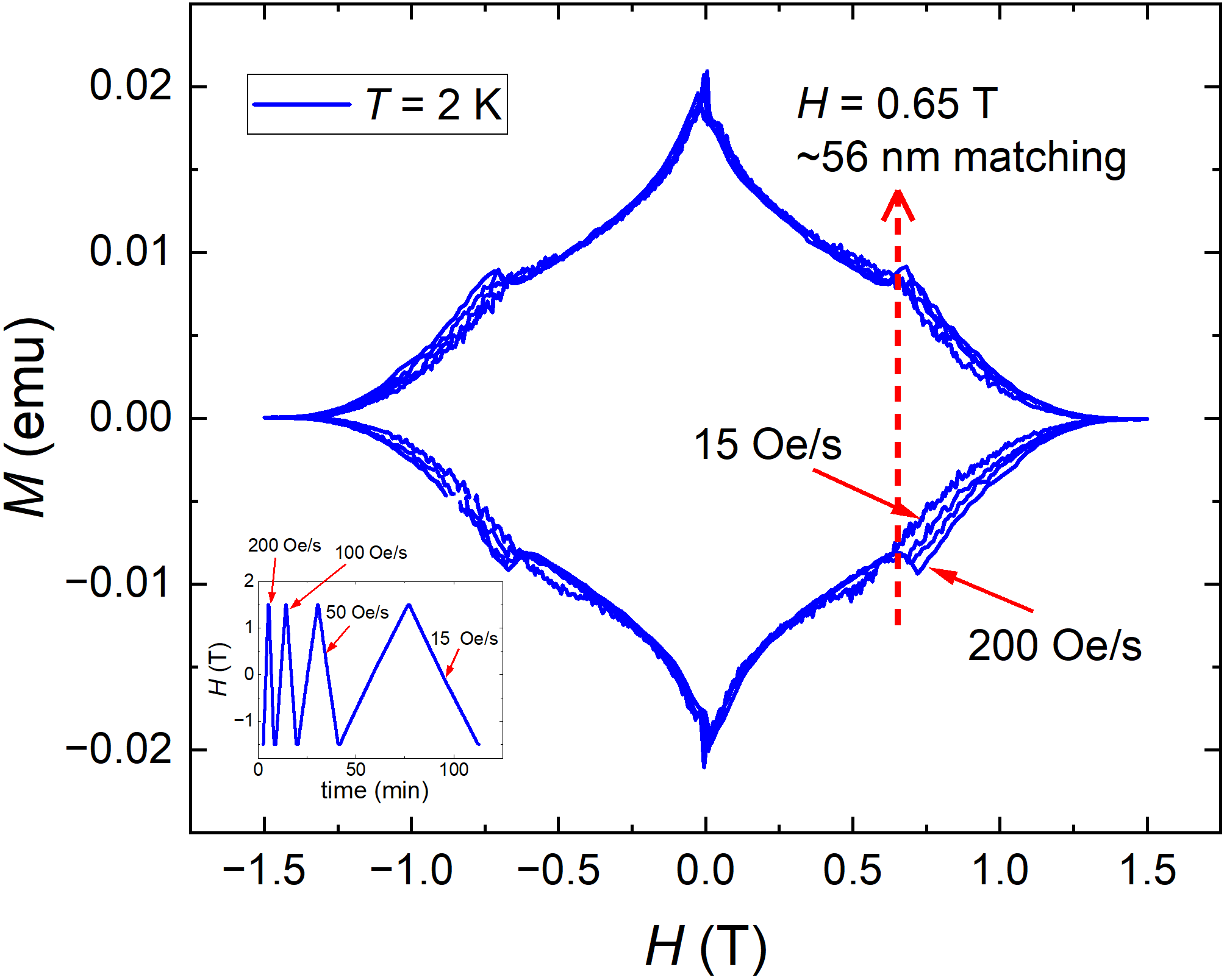
Figure 4 shows profound features on the magnetic hysteresis loops obtained using Quantum Design PPMS-VSM. This instrument allows for the measurements while sweeping the magnetic field continuously without pausing. The field time variation is shown in the inset with 200, 100, 50, and 15 Oe/s rates, more than ten times the span of . The measurements shown in 4 were performed perpendicular to the film plane. Figure 4 shows additional dynamic rate-dependent hysteretic response appearing above roughly 0.65 T. In the simplest approximation, if the average distance between Abrikosov vortices is , it corresponds to the magnetic induction of , where Wb is the magnetic flux quantum. If there are some pinning centers of a characteristic length-scale, , the vortex pinning is most efficient when the inter-vortex distance matches this scale, . This defines the “matching field”, . Therefore, we can estimate nm, where, in our case, T, Fig.4. This immediately reminds of Fig.1 where this length scale was determined from the direct EM imaging, providing further evidence of the importance of the film morphology in determining the magnetic response. Overall, our films show a much larger magnetic hysteresis compared to the bulk samples and single crystals [36, 43]. However, a very large demagnetizing factor and thin-film geometry play a significant role in diminishing the interval and the magnitude of the reversible magnetic moment, which is proportional to a very small film volume, whereas irreversible Bean currents flow in the entire sample [44, 45, 46, 47, 48].
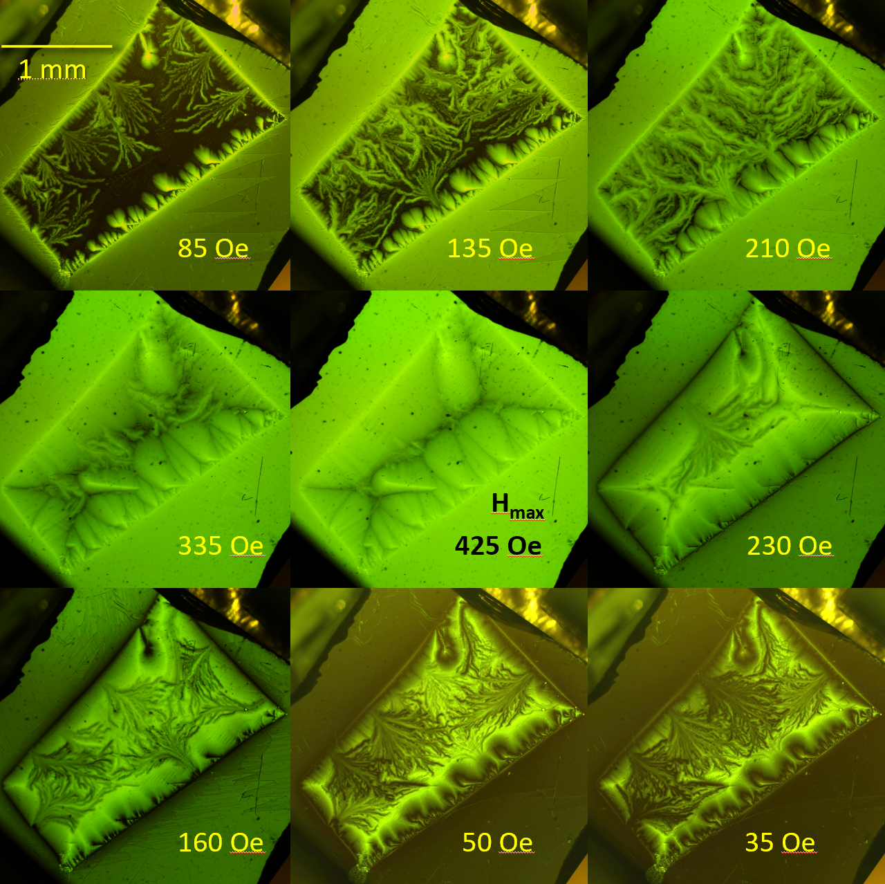
We now examine the details of the magnetic flux penetration and exit using direct magneto-optical imaging of the superconducting state using specially fabricated transparent ferrimagnetic indicators placed on top of samples [31, 49, 50]. Figure 5 shows the sequence of images obtained after cooling in zero magnetic field to 5 K. The first five frames (left to right, top to bottom) show increasing magnetic field up to the maximum of Oe, after which the magnetic field was reduced, and flux was exiting the sample. There are two distinct regimes of flux penetration and exit. First, large-scale, very fast (see the video in supplemental information), dendritic avalanches similar in their appearance to lightning strikes. Similar behavior was observed long ago in various films, particularly niobium, and is well-understood [51, 52]. The physics behind it is straightforward. When first vortices are pushed inside by the screening currents, these moving vortices induce an electric field parallel to the currents, resulting in a resistive state, and energy is dissipated. If there is an insufficient thermal link to the surrounding and, in the case of films, to the substrate, the released heat decreases the local critical current in the direction of the vortex motion creating a self-heating violent unidirectional propagation of bunches of vortices that follow the heated up trail which needs time to dissipate. Sometimes they branch out when meeting various obstacles and, in this case, most likely the grain boundaries. In thicker samples (a few tens of m foils), the avalanches may become “global” leading to a catastrophic collapse of the entire Bean critical state [50]. The actual local temperature instabilities have been measured during these processes. In the case of QIS applications, this insufficient heat channeling may represent a difficult problem. The second stage of flux penetration is a regular Bean critical state pattern [44, 45, 47], also somewhat non-uniform, following the granular film morphology. When the external magnetic field is decreased, the reverse process happens, and similar dendritic avalanches start to channel out, now shown by a darker color corresponding to the local suppression of the magnetic induction. In the end, the mix of uniform and non-uniform trapped flux remains in the sample as a fingerprint of the intense perturbations occurring when the field was ramped up and down. The supplemental information shows a real-time movie of the processes pictured in Fig.5. This highly inhomogeneous magnetic flux evolution reveals the issues of thermal heat-sinking and morphological inhomogeneity issues.
IV Discussion
Let us review the experimental findings and try to understand all different results from a common point of view. All measurements indicate that as far as superconducting properties are concerned, the films are rather far from being ideal and exhibit various irreversible properties that generally lead to dissipation, hence quantum decoherence.
One of the most puzzling facts is that while the is rather very low, the superconducting transition temperature, K, is as high as in good single crystals. According to the theory, should be suppressed by non-magnetic disorder due to anisotropy of the order parameter and a multi-band nature of the material [38]. However, the same theory predicts saturation of the when the gap averages out at higher scattering rates. Still, should be lower than 9 K, and it isn’t. One natural way to understand it, supported by the direct EM imaging, Fig.1, is to assume that grains themselves are quite clean in terms of the scattering rate, but the random network of grain boundaries creates significant resistance. The boundaries do not affect high inside the grains, though. In the normal state, just above , the resistivity is mostly determined by those boundaries. However, when the grains become superconducting, the boundaries become a network of Josephson junctions, and the whole sample transitions to zero resistance. This explains the low and, simultaneously, high .
The heterogeneous granular structure also explains the measurements of the third and the upper critical fields, shown in Fig.2. While it is important to measure these two fields in one experiment and on the same sample, the problem is that their ratio is about 1.3, whereas a ratio of at least 1.7 is expected theoretically even in the dirty limit [39]. However, real sample geometry and surface conditions may significantly affect the [29] beyond the point-like scattering and smooth semi-infinite surface with perfectly parallel field considered in Ref.[39]. Therefore, our granular film does not show the expected maximum value of this ratio. This is further re-enforced by the clear matching effect at the length-scale of around 50 nm, Fig.4, which correlates with the granular structure revealed by the film electron microscopy, Fig.1.
Finally, the thermo-magnetic instabilities found in our study indicate an impeded heat flow and removal in these films. While QIS applications of thin films do not use an external magnetic field, the transmons are driven at high frequencies and show elevated dissipation due to morphological inhomogeneities. In particular, the granular structure may contribute to their additional distortion of the current flow, and extra resistance [53, 54]. Another possible source is Kapitza resistance due to phonon flow mismatch at the boundaries and the interfaces [54]. Finally, occasional vortices may enter the structure due to extreme demagnetization and sharp edges. With or without vortices, the heat dissipation and cooling may become a serious issue if the device is located in a high vacuum and can only sink heat through a substrate.
On the bright side, the films show clean exponential attenuation of the weak magnetic field, signaling a fairly clean superconducting gap. Therefore, they still have the potential for improvement, and here we suggest some strategies.
IV.1 Suggested mitigation strategies
A few suggestions can be made regarding applying such films for superconducting transmons. (1) To investigate the impeded heat transfer and dissipation, one may try to measure the coherence time by comparing the same transmon in vacuum and immersed in liquid helium directly inside a mixing chamber of a dilution refrigerator. (2) Reducing the substrate thickness may help to improve heat sinking when transmons are in a vacuum. (3) The most problematic aspect of these films is that their granular structure may be fixed by switching to a different deposition method. The alternative methods producing better Nb films have been known since the 1980s [55, 56]. For example, molecular beam epitaxy (MBE) was shown to produce Nb films of excellent crystallinity with and, remarkably, K [55]. In this case, different substrates, better matching Nb thermal contraction and expansion, such as Al2O3 and MgO were used. (4) One may also try to perform post-manufacturing treatment of the prepared films, for example, using recently introduced electro-annealing that was used for the optimization of quantum interference devices [57]. (5) Finally, we recently showed [58] that the introduction of true point-like defects using proton irradiation expectedly reduces the somewhat, to around 9.16 K, indicating that it affects the grains’ interior. However, it seems to also inhibit thermo-magnetic instabilities, perhaps because these defects increase critical current density, thus reducing vortex motion. Uniformly distributed, dilute point-like defects may be beneficial for the transmons for other reasons. For example, they may reduce (pin or alter otherwise) the activity of two-level systems (TLS) and also prevent phase slips in the Josephson network of grain boundaries.
V Conclusions
In summary, a comprehensive characterization of 160 nm thick Nb films on [001] Si substrate used in superconducting transmons is presented. Electron microscopy, transport, magnetization, quasiparticle spectroscopy, and real-space magneto-optical images all show that while these films have outstanding superconducting transition temperature of K and clean superconducting gap, their behavior in the magnetic field is complicated exhibiting significantly irreversible behavior, and insufficient heat conductance leading to thermo-magnetic instabilities. These may present an issue for further improvement of transmon quantum coherence. Possible mitigation strategies are suggested, and the techniques presented here provide guidelines for comprehensive characterization that may be used to improve materials for superconducting quantum computing.
Acknowledgements.
We thank V. Kogan, M. Zarea, A. Romanenko, and A. Grasselino for discussions and attention. We thank the Rigetti fabrication team for developing and manufacturing the studied films. This work was supported by the U.S. Department of Energy, Office of Science, National Quantum Information Science Research Centers, Superconducting Quantum Materials and Systems Center (SQMS) under contract number DE-AC02-07CH11359. The research was performed at the Ames National Laboratory, operated for the U.S. DOE by Iowa State University under contract # DE-AC02-07CH11358.References
- Reagor et al. [2016] M. Reagor, W. Pfaff, C. Axline, R. W. Heeres, N. Ofek, K. Sliwa, E. Holland, C. Wang, J. Blumoff, K. Chou, M. J. Hatridge, L. Frunzio, M. H. Devoret, L. Jiang, and R. J. Schoelkopf, Quantum memory with millisecond coherence in circuit QED, Physical Review B 94, 014506 (2016).
- Kjaergaard et al. [2020] M. Kjaergaard, M. E. Schwartz, J. Braumüller, P. Krantz, J. I.-J. Wang, S. Gustavsson, and W. D. Oliver, Superconducting qubits: Current state of play, Annual Review of Condensed Matter Physics 11, 369 (2020), https://doi.org/10.1146/annurev-conmatphys-031119-050605 .
- Alam and et al [2022] M. S. Alam and et al, Quantum computing hardware for hep algorithms and sensing, arXiv:2204.08605 (2022), arXiv:2204.08605 [quant-ph] .
- Jurcevic et al. [2021] P. Jurcevic, A. Javadi-Abhari, L. S. Bishop, I. Lauer, D. F. Bogorin, M. Brink, L. Capelluto, O. Günlük, T. Itoko, N. Kanazawa, A. Kandala, G. A. Keefe, K. Krsulich, W. Landers, E. P. Lewandowski, D. T. McClure, G. Nannicini, A. Narasgond, H. M. Nayfeh, E. Pritchett, M. B. Rothwell, S. Srinivasan, N. Sundaresan, C. Wang, K. X. Wei, C. J. Wood, J.-B. Yau, E. J. Zhang, O. E. Dial, J. M. Chow, and J. M. Gambetta, Demonstration of quantum volume 64 on a superconducting quantum computing system, Quantum Science and Technology 6, 025020 (2021).
- de Leon et al. [2021] N. P. de Leon, K. M. Itoh, D. Kim, K. K. Mehta, T. E. Northup, H. Paik, B. S. Palmer, N. Samarth, S. Sangtawesin, and D. W. Steuerman, Materials challenges and opportunities for quantum computing hardware, Science 372, eabb2823 (2021), https://www.science.org/doi/pdf/10.1126/science.abb2823 .
- Schlör et al. [2019] S. Schlör, J. Lisenfeld, C. Müller, A. Bilmes, A. Schneider, D. P. Pappas, A. V. Ustinov, and M. Weides, Correlating decoherence in transmon qubits: Low frequency noise by single fluctuators, Phys. Rev. Lett. 123, 190502 (2019).
- Lee et al. [2021] J. Lee, Z. Sung, A. A. Murthy, M. Reagor, A. Grassellino, and A. Romanenko, Discovery of nb hydride precipitates in superconducting qubits, arXiv:2108.10385 (2021), arXiv:2108.10385 [quant-ph] .
- Murthy et al. [2022] A. A. Murthy, J. Lee, C. Kopas, M. J. Reagor, A. P. McFadden, D. P. Pappas, M. Checchin, A. Grassellino, and A. Romanenko, Tof-sims analysis of decoherence sources in superconducting qubits, Applied Physics Letters 120, 044002 (2022), https://doi.org/10.1063/5.0079321 .
- Müller et al. [2019] C. Müller, J. H. Cole, and J. Lisenfeld, Towards understanding two-level-systems in amorphous solids: insights from quantum circuits, Reports on Progress in Physics 82, 124501 (2019).
- Oliver and Welander [2013] W. D. Oliver and P. B. Welander, Materials in superconducting quantum bits, MRS Bulletin 38, 816 (2013).
- Wang et al. [2015] C. Wang, C. Axline, Y. Y. Gao, T. Brecht, Y. Chu, L. Frunzio, M. H. Devoret, and R. J. Schoelkopf, Surface participation and dielectric loss in superconducting qubits, Applied Physics Letters 107, 162601 (2015).
- Dial et al. [2016] O. Dial, D. T. McClure, S. Poletto, G. A. Keefe, M. B. Rothwell, J. M. Gambetta, D. W. Abraham, J. M. Chow, and M. Steffen, Bulk and surface loss in superconducting transmon qubits, Superconductor Science and Technology 29, 044001 (2016).
- Gambetta et al. [2017] J. M. Gambetta, C. E. Murray, Y. K. K. Fung, D. T. McClure, O. Dial, W. Shanks, J. W. Sleight, and M. Steffen, Investigating surface loss effects in superconducting transmon qubits, IEEE Transactions on Applied Superconductivity 27, 1 (2017).
- Burnett et al. [2016] J. Burnett, L. Faoro, and T. Lindstrom, Analysis of high quality superconducting resonators: consequences for TLS properties in amorphous oxides, Superconductor Science and Technology 29, 044008 (2016).
- Niepce et al. [2020] D. Niepce, J. J. Burnett, M. G. Latorre, and J. Bylander, Geometric scaling of two-level-system loss in superconducting resonators, Superconductor Science and Technology 33, 025013 (2020).
- Verjauw et al. [2021] J. Verjauw, A. Potočnik, M. Mongillo, R. Acharya, F. Mohiyaddin, G. Simion, A. Pacco, T. Ivanov, D. Wan, A. Vanleenhove, L. Souriau, J. Jussot, A. Thiam, J. Swerts, X. Piao, S. Couet, M. Heyns, B. Govoreanu, and I. Radu, Investigation of microwave loss induced by oxide regrowth in high-q niobium resonators, Phys. Rev. Applied 16, 014018 (2021).
- Premkumar et al. [2021] A. Premkumar, C. Weiland, S. Hwang, B. Jaeck, A. Place, I. Waluyo, A. Hunt, V. Bisogni, J. Pelliciari, A. Barbour, M. Miller, P. Russo, F. Camino, K. Kisslinger, X. Tong, M. Hybertsen, A. Houck, and I. Jarrige, Microscopic relaxation channels in materials for superconducting qubits, Communications Materials 2, 10.1038/s43246-021-00174-7 (2021).
- Anderson [1959] P. W. Anderson, Theory of dirty superconductors, Journal of Physics and Chemistry of Solids 11, 26 (1959).
- Arai and Kita [2004] M. Arai and T. Kita, Ab initio calculations of hc2 for nb, nbse2, and mgb2, Journal of the Physical Society of Japan 73, 2924 (2004).
- Bahte et al. [1998] M. Bahte, F. Herrmann, and P. Schmuser, Magnetization and susceptibility measurements on niobium samples for cavity production, Part. Accel. 60, 121 (1998).
- Barkov et al. [2013] F. Barkov, A. Romanenko, Y. Trenikhina, and A. Grassellino, Precipitation of hydrides in high purity niobium after different treatments, Journal of Applied Physics 114, 164904 (2013).
- Barkov et al. [2012] F. Barkov, A. Romanenko, and A. Grassellino, Direct observation of hydrides formation in cavity-grade niobium, Physical Review Special Topics - Accelerators and Beams 15, 122001 (2012).
- Dhakal et al. [2017] P. Dhakal, G. Ciovati, and G. R. Myneni, Role of thermal resistance on the performance of superconducting radio frequency cavities, Physical Review Accelerators and Beams 20, 032003 (2017).
- Valente-Feliciano et al. [2022] A. M. Valente-Feliciano, C. Antoine, S. Anlage, G. Ciovati, J. Delayen, F. Gerigk, A. Gurevich, T. Junginger, S. Keckert, G. Keppe, J. Knobloch, T. Kubo, O. Kugeler, D. Manos, C. Pira, T. Proslier, U. Pudasaini, C. E. Reece, R. A. Rimmer, G. J. Rosaz, T. Saeki, R. Vaglio, R. Valizadeh, H. Vennekate, W. V. Delsolaro, M. Vogel, P. B. Welander, and M. Wenskat, Next-generation superconducting rf technology based on advanced thin film technologies and innovative materials for accelerator enhanced performance and energy reach, arXiv:2204.02536 (2022), arXiv:2204.02536 [physics.acc-ph] .
- Oh et al. [2022] J.-S. Oh, X. Fang, T.-H. Kim, M. Lynn, M. Kramer, M. Zarea, J. A. Sauls, A. Romanenko, S. Posen, A. Grassellino, C. J. Kopas, M. Field, J. Marshall, H. Cansizoglu, J. Y. Mutus, M. Reagor, and L. Zhou, Multi-modal electron microscopy study on decoherence sources and their stability in nb based superconducting qubit, arXiv:2204.06041 (2022), arXiv:2204.06041 [cond-mat.mtrl-sci] .
- Prozorov and Giannetta [2006] R. Prozorov and R. W. Giannetta, Magnetic penetration depth in unconventional superconductors, Superconductor Science and Technology 19, R41 (2006).
- Prozorov and Kogan [2011] R. Prozorov and V. G. Kogan, London penetration depth in iron-based superconductors, Reports on Progress in Physics 74, 124505 (2011).
- Abrikosov [2017] A. A. Abrikosov, Fundamentals of the Theory of Metals (Dover Publications, Newburyport, 2017).
- Kogan et al. [2002] V. G. Kogan, J. R. Clem, J. M. Deang, and M. D. Gunzburger, Nucleation of superconductivity in finite anisotropic superconductors and the evolution of surface superconductivity toward the bulk mixed state, Physical Review B 65, 094514 (2002).
- Liu et al. [2013] Y. Liu, M. A. Tanatar, V. G. Kogan, H. Kim, T. A. Lograsso, and R. Prozorov, Upper critical field of high-quality single crystals of kfe2as2, Phys. Rev. B 87, 134513 (2013).
- Indenbom et al. [1993] M. V. Indenbom, T. Schuster, M. R. Koblischka, A. Forkl, H. Kronmueller, L. A. Dorosinskii, V. K. Vlasko-Vlasov, A. A. Polyanskii, R. L. Prozorov, and V. I. Nikitenko, Study of flux distributions in high-Tc single crystals and thin films using magnetooptic techniques, Physica C 209, 259 (1993).
- Prozorov et al. [2005] R. Prozorov, R. W. Giannetta, A. A. Polyanskii, and G. K. Perkins, Topological hysteresis in the intermediate state of type-I superconductors, Phys. Rev. B 72, 212508 (2005).
- Prozorov [2007] R. Prozorov, Equilibrium topology of the intermediate state in type-I superconductors of different shapes, Phys. Rev. Lett. 98, 257001 (2007).
- Prozorov et al. [2008] R. Prozorov, A. Fidler, J. Hoberg, and P. Canfield, Suprafroth in type-i superconductors, Nature Physics 4, 327 (2008).
- Liarte et al. [2017] D. B. Liarte, S. Posen, M. K. Transtrum, G. Catelani, M. Liepe, and J. P. Sethna, Theoretical estimates of maximum fields in superconducting resonant radio frequency cavities: stability theory, disorder, and laminates, Superconductor Science and Technology 30, 033002 (2017).
- Finnemore et al. [1966] D. K. Finnemore, T. F. Stromberg, and C. A. Swenson, Superconducting properties of high-purity niobium, Physical Review 149, 231 (1966).
- Lechner et al. [2020] E. M. Lechner, B. D. Oli, J. Makita, G. Ciovati, A. Gurevich, and M. Iavarone, Electron tunneling and x-ray photoelectron spectroscopy studies of the superconducting properties of nitrogen-doped niobium resonator cavities, Physical Review Applied 13, 044044 (2020).
- Zarea et al. [2022] M. Zarea, H. Ueki, and J. A. Sauls, Effects of anisotropy and disorder on the superconducting properties of niobium, arXiv:2201.07403 (2022), arXiv:2201.07403 [cond-mat.supr-con] .
- Xie et al. [2017] H.-Y. Xie, V. G. Kogan, M. Khodas, and A. Levchenko, Onset of surface superconductivity beyond the saint-james–de gennes limit, Physical Review B 96, 104516 (2017).
- Koethe and Moench [2000] A. Koethe and J. I. Moench, Preparation of ultra high purity niobium, Materials Transactions, JIM 41, 7 (2000).
- Bardeen et al. [1957] J. Bardeen, L. N. Cooper, and J. R. Schrieffer, Microscopic theory of superconductivity, Physical Review 106, 162 (1957).
- Prozorov [2021] R. Prozorov, Meissner-london susceptibility of superconducting right circular cylinders in an axial magnetic field, Physical Review Applied 16, 024014 (2021).
- Stromberg [1965] T. F. Stromberg, The superconducting properties of high purity niobium, Ph.D. thesis, Iowa State University (1965).
- Bean [1962] C. P. Bean, Magnetization of hard superconductors, Phys. Rev. Lett. 8, 250 (1962).
- Bean [1964] C. P. Bean, Magnetization of high-field superconductors, Rev. Mod. Phys. 36, 31 (1964).
- Brandt [1995] E. H. Brandt, The flux-line lattice in superconductors, Reports on Progress in Physics 58, 1465 (1995).
- Brandt [1998] E. H. Brandt, Superconductor disks and cylinders in an axial magnetic field. I. Flux penetration and magnetization curves, Phys. Rev. B - Condens. Matter Mater. Phys. 58, 6506 (1998).
- Brandt [1996] E. H. Brandt, Superconductors of finite thickness in a perpendicular magnetic field: Strips and slabs, Phys. Rev. B 54, 4246 (1996).
- Young et al. [2005] D. P. Young, M. Moldovan, P. W. Adams, and R. Prozorov, Magneto-optical studies of flux penetratim in super-hard Nb wire, Superc. Sci. Technol. 18, 776 (2005).
- Prozorov et al. [2006] R. Prozorov, D. V. Shantsev, and R. G. Mints, Collapse of the critical state in superconducting niobium, Phys. Rev. B 74, 220511 (2006).
- Blanco Alvarez et al. [2019] S. Blanco Alvarez, J. Brisbois, S. Melinte, R. B. G. Kramer, and A. V. Silhanek, Statistics of thermomagnetic breakdown in nb superconducting films, Scientific Reports 9, 3659 (2019).
- Vestgården et al. [2018] J. I. Vestgården, T. H. Johansen, and Y. M. Galperin, Nucleation and propagation of thermomagnetic avalanches in thin-film superconductors (review article), Low Temperature Physics 44, 460 (2018), https://doi.org/10.1063/1.5037549 .
- Ramiere et al. [2022] A. Ramiere, C. Z. Antoine, and J. Amrit, Model for hot spots and -slope behavior in granular niobium thin film superconducting rf cavities, Phys. Rev. Accel. Beams 25, 022001 (2022).
- Mizuno and Aomine [1984] K. Mizuno and T. Aomine, Current induced hotspot in superconducting thin films with different thicknesses, Journal of the Physical Society of Japan 53, 1434 (1984), https://doi.org/10.1143/JPSJ.53.1434 .
- ichiro Oya et al. [1986] G. ichiro Oya, M. Koishi, and Y. Sawada, High-quality single-crystal nb films and influences of substrates on the epitaxial growth, Journal of Applied Physics 60, 1440 (1986).
- Wagner [1998] T. Wagner, High temperature epitaxial growth and structure of nb films on alpha-al2o3 (0001), Journal of Materials Research 13, 693 (1998).
- Collienne et al. [2021] S. Collienne, B. Raes, W. Keijers, J. Linek, D. Koelle, R. Kleiner, R. B. Kramer, J. Van de Vondel, and A. V. Silhanek, Nb - based nanoscale superconducting quantum interference devices tuned by electroannealing, Phys. Rev. Applied 15, 034016 (2021).
- Tanatar et al. [2022] M. A. Tanatar, D. Torsello, K. R. Joshi, S. Ghimire, M. Zarea, C. J. Kopas, G. Ghigo, J. A. Sauls, and R. Prozorov, Anisotropic superconductivity of niobium from the response to artificial disorder, in preparation (2022).