Robust incorporation in multi-donor patches created using \phrase
Abstract
Atomic-precision advanced manufacturing enables the placement of dopant atoms within 1 lattice site in crystalline Si. However, it has recently been shown that reaction kinetics can introduce uncertainty in whether a single donor will incorporate at all in a minimal 3-dimer lithographic window. In this work, we explore the combined impact of lithographic variation and stochastic kinetics on P incorporation as the size of such a window is increased. We augment a kinetic model for PH3 dissociation leading to P incorporation on Si(100)-21 to include barriers for reactions across distinct dimer rows. Using this model, we demonstrate that even for a window consisting of 23 silicon dimers, the probability that at least one donor incorporates is nearly unity. We also examine the impact of size of the lithographic window, finding that the incorporation fraction saturates to -layer like coverage as the circumference-to-area ratio approaches zero. We predict that this incorporation fraction depends strongly on the dosage of the precursor, and that the standard deviation of the number of incorporations scales as , as would be expected for a series of largely independent incorporation events. Finally, we characterize an array of experimentally prepared multi-donor lithographic windows and use our kinetic model to study variability due to the observed lithographic roughness, predicting a negligible impact on incorporation statistics. We find good agreement between our model and the inferred incorporation in these windows from scanning tunneling microscope measurements, indicating the robustness of \phrase to errors in patterning for multi-donor patches.
HRL Laboratories, LLC, Malibu, CA 90265, USA \altaffiliationIBM Quantum, IBM T.J. Watson Research Center, Yorktown Heights, NY 10598, USA
![[Uncaptioned image]](/html/2207.10631/assets/x1.png)
1 Introduction
Atomic-precision advanced manufacturing (APAM) is a suite of techniques for fabricating Si nanoelectronic devices for applications ranging from analog quantum simulators 1, 2, 3, 4, 5, 6, 7, to qubits 8, 9, 10, 11, 12, 13, 14, to digital electronics 15, 16. APAM-fabricated devices are comprised of lithographically defined dopant structures with features that nominally have resolutions at the limit of a single-atomic site ( Å). While this resolution has been demonstrated for the placement of single dopant atoms 17, this manuscript examines the extent to which it persists for larger dopant structures in the presence of stochastic incorporation and lithographic imperfection.
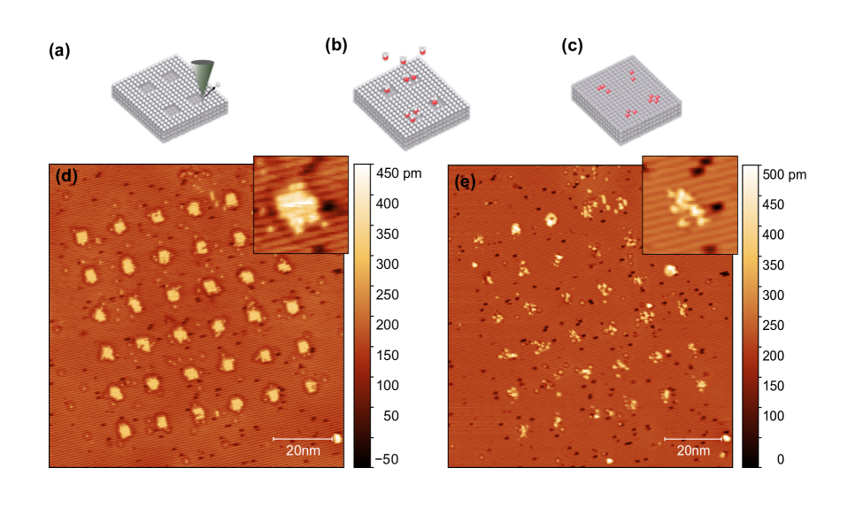
In contrast to doping via conventional ion implantation, APAM methods introduce dopants through a window in an atomically thin lithographic resist (e.g., a passivating layer of hydrogen). Fig.1 (a) shows a window created by H depassivation lithography (HDL) in which a scanning tunneling microscope (STM) tip is used to remove the H-resist with atomic precision. Then, as in Fig.1 (b), dopant atoms are introduced by exposing the templated surface to a flux of a gas-phase precursor. During a subsequent anneal, dopants incorporate into the Si, Fig.1 (c). Lateral dopant diffusion across the surface is bounded by the HDL template, while dopants are constrained to the surface layer by keeping the process temperature low ( K) to activate surface chemistry, while leaving bulk diffusion inactive. STM images of the process reveal atomic-scale roughness in feature shapes at the HDL step, Fig.1 (d) inset, and in the ultimate doping outcome, Fig.1 (e). The extent to which this is due to lithographic imperfection and/or stochastic incorporation kinetics is the question that we seek to answer.
It is worth emphasizing that this style of APAM fabrication relies on a relatively complicated sequence of surface chemical reactions for which the balance among the rates determine the ultimate stochastic incorporation outcome. Each step requires activation over a kinetic barrier that is significant compared to energetic differences between the initial and final states. Further, in many of the intermediate states, more than one reaction is simultaneously accessible enhancing the prospect for a random outcome. Thus we expect variability among samples in any ensemble depending on the probability of successful incorporation, . It has been empirically observed that delta layers achieve 1/4 P coverage and thus we can approximate a single incorporation event in a sufficiently large pattern as having a probability . To the extent that we can treat each possible P incorporation event as a single Bernoulli trial with probability (i.e., it either incorporates or does not with independent of other events) we expect the variance (standard deviation) in the number of dopants in a structure consisting of atoms to be (). For () the ensemble variability in will be negligible because the process will be deterministic, but for this variability will be strongest. In this manuscript we predict that – for our process, and thus variability in the number of dopant atoms in a nominally atom structure is significant.
There are relatively few examples of studies of the ensemble variability of APAM-fabricated structures 18, 19. However, such studies are becoming increasingly relevant with the growing drive to scale up APAM-fabricated devices like quantum processors, analog quantum simulators, and classical electronic components/circuits. In each of these technologies there is significant interest in architectures based on structures comprised of few-dopant clusters for which variance in the number of dopants might substantially change the on-site energy of the dopant clusters. This could lead to substantial randomness in the properties of an array of such few-dopant clusters, making controlled quantum devices less achievable using this methodology. Recent work in the field has selected the size of APAM engineered quantum dots specifically to avoid statistical variation in the number of dopants 20. By better understanding incorporation kinetics we can treat variance in the number of incorporations in a small window as a new engineering degree of freedom. This might enable robust device functionalities that continue to operate subject to this particular source of variability.
Here, we report the analysis of an ensemble of APAM windows and their incorporation statistics, relying on kinetic simulations of nanoscale lithographic features to understand the variability of doping outcomes for nominally identical nanostructures. We predict that for small dimer windows, we should see at least one incorporation for all windows larger than 23 silicon dimers in size. For larger windows, we predict that the fraction of sites incorporated quickly saturates as the circumference-to-area ratio decreases. Finally, we measure the experimental lithographic error on a number of 3 nm 3 nm wide arrays. We then use our kinetic model to predict the impact of this lithographic error on the system, finding good agreement with experimental results. These indicate that lithographic errors tend to have a small impact on the final system compared to the inherent chemical reaction path dependent stochasticity. Our simulations shows that while varying incorporation pathways can lead to stochastic results for single donor arrays, at larger sizes, these APAM fabricated arrays are largely robust to both chemical and lithographic variation. This implies that APAM multi-donor arrays can reliably be used in the construction of quantum dot devices in larger scale quantum computing and analog simulation.
2 Results
To study the incorporation statistics of HDL-fabricated windows we augmented a Kinetic Monte Carlo (KMC) model first demonstrated by Ivie, Campbell, and Koepke et al.21. This prior work only considered reactions within a single dimer-row and thus the chemistry was expanded to include reactions that become possible in larger windows, particularly PH3 dissociation reactions taking place across rows. Warschkow et al. demonstrated the first of these steps with a PH3 molecule losing a hydrogen atom to a different silicon dimer-row (as opposed to losing the hydrogen to another dimer along the same row) 22. However, an exhaustive set of inter-row reactions has not been comprehensively explored. We use density functional theory to calculate the reaction barriers for a large number of these reactions, with further details in Appendix A. We then include these reactions, along with the previously calculated reactions from Warschkow et al. 22 in the KMC model from Ivie, Campbell, and Koepke et al.21. More details of this kinetic model are given in Appendix B. The source code for these simulations is available on github 23.
2.1 Incorporation in small multi-donor clusters
We first focus on small windows that only allow donors to incorporate. For single-donor incorporation, it is common to create a window on one silicon dimer-row that is three dimers long 24. This provides sufficient room for one PH3 molecule to adsorb and then shed hydrogen to the surrounding silicon atoms before incorporating. While this suggests a clear route to single-donor incorporation, at typical room-temperature dosing conditions there is a probability that the associated P atom will fail to incorporate 25, seemingly due to interference with another adsorbed PH3 21. It is worth noting that other experiments have observed more favorable single-donor incorporation probabilities for smaller sample sizes 26. These aren’t inconsistent with data from larger samples, but they suggest that inference of the incorporation rate might be subject to systematic uncertainty that isn’t yet fully understood. This uncertainty notwithstanding, we should expect that expanding the three-dimer window used for single-donor incorporation will allow for more PH3 atoms to adsorb and dissociate, making it much more likely that at least one donor will incorporate within the window. We thus consider “small” windows as starting at three silicon dimers and expanding to include windows for which we expect donors to incorporate.
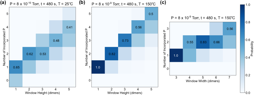
In Fig. 2a, we show predictions from our kinetic model for the probability of incorporating 1 to 5 atoms in a window three dimers wide along a row, as a function of the number of silicon dimer rows included in the window (i.e., 13, 23, 33, etc.). The number of possible incorporations varies across different window sizes. For both a 23 and 33 window, the most likely number of P incorporations is two, with a probability of 62% and 53%, respectively. For all windows larger than 23, the range of possible incorporations is at least three. Notably, even at the room-temperature dosing conditions, we predict only a neglible 0.2% chance of zero P atoms incorporating in any windows more than 2 dimers rows and 3 dimers within a row. This confirms what one might intuitively expect– that creating larger windows is an effective strategy for guaranteeing that every element in an array comprised of multi-donor patches has at least one donor. Our predictions suggest a lower bound on the window dimension for which this strategy will work.
Based on conditions predicted to lead to deterministic incorporation in our previous work, we also explore the same window sizes while using a higher temperature of during dosing. We predicted this arrangement would lead to deterministic incorporation for a single donor in the case of a 13 window 21. As shown in Fig. 2b, however, this elevated temperature dosing is not predicted to remain deterministic at larger patch sizes. While the number of expected incorporation events reliably shifts up, the probability of achieving as many donor incorporations as the number of depassivated sites would suggest decreases as the size of the window increases. This stochasticity can be entirely attributed to the new reactions across dimer rows introduced in Sec. Appendix C: 3 3 nm heatmaps of incorporation. Without these reactions, a 53 dimer window would be exactly equivalent to five separate 13 windows and five deterministic incorporation events would be expected at the elevated temperature dosing conditions under consideration. This shows that reactions across dimer rows are competitive with reactions along dimer rows and further that these reactions can lead to site blocking, preventing the dissociation of some of the adsorbed PH3 molecules.
We finally examine windows oriented along a single dimer-row, but with different widths in Fig. 2c. We again use the elevated temperature conditions associated with the deterministic incorporation of a single donor for a 13 window. We again see, however, that the deterministic nature of incorporation is limited to the 13 window providing exactly enough space for one molecule to dissociate. As the width of the window increases, more than one PH3 has room to dissociate within it. This might lead to multiple incorporations, but interference among adsorbed molecules might also prevent all incorporations but one. Notably, a 16 window does not behave the same as two 13 windows, there is still a 7.6% chance that only a single donor will incorporate. This stochasticity brings both the promise of more potential incorporations and the danger of fewer. A 16 window has a 26.8% chance of three donors incorporating if the adsorption and dissociation proceeds just right, which would not be possible in two separated 13 windows. Critically, this disorder does not lead to any configurations where zero incorporation events are predicted.
2.2 Size-dependence of incorporation in larger multi-donor clusters
One important question facing kinetic models of the APAM doping process is how to assign surface dissociation outcomes as leading to P incorporation. While the initial steps of PH3 dissociation on the silicon surface have been well mapped out by Warschkow et al. 22 and extended in Appendix A, modeling the full substitutional incorporation process once the P atom moves below the surface is computationally prohibitive. In our previous work, we used a bridging PH fragment as a proxy for incorporation. This was because its significant adsorption energy makes negligible the likelihood of the P atom desorbing during subsequent anneals 21. We further showed that this choice of incorporation proxy led to good agreement with the experimentally inferred incorporation rate based on STM images taken after an incorporation anneal. An analogous choice of bridging BH and BCl as incorporation proxies has also aligned with electrically measured incorporation rates for diborane and boron trichoride precursors 27, 28.
Nevertheless, this choice of incorporation proxy raises an important question– where does the final H on the bridging PH molecule go before incorporation? If it is shed onto the surface it could prevent the further dissociation of nearby PH3 molecules and fragments thereof, potentially lowering the overall incorporation rate. On the other hand, if the H is abstracted toward the surface within the post-anneal growth process and the P subsequently incorporates, then this process could likely also be extended to a less stringent proxy of PH2. To investigate this question, we examine the size dependence of APAM incorporation rates using multiple different proxies for incorporation.
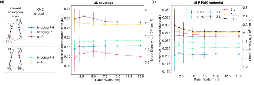
Fig. 3a compares the incorporation rates predicted using different proxies for incorporation and allowed adsorption sites as a function of the size of a square depassivated window with dosing conditions providing a 3 Langmuir (L) dose. We predict that once the lithographic window for atomic-precision exceeds 5 nm, the mean incorporation rate per unit area is practically constant for most incorporation proxies. The higher degree of change in the mean incorporation fraction at patch widths below 5 nm can likely be attributed to edge effects being relatively more important in smaller systems, where the circumference-to-area ratio is higher. As expected, the asymptotic density of incorporations is lower when using a bridging P atom as a proxy for incorporation instead of a bridging PH molecule.
We note that the fraction of a monolayer covered by incorporations for both the bridging PH and bridging P proxies (0.1 ML and 0.15 ML, respectively) is below the 0.25 ML figure from the literature. To investigate the limits of varying the incorporation proxy, we also consider a proxy for incorporation in which all of the P on the surface eventually incorporates, i.e. even P atoms that are locked in PH3 or PH2 configurations will be counted as incorporating. This is an overestimate of the actual number of incorporations as we are assuming perfect incorporation of molecules that have not completely dissociated and are likely to migrate. In this case, we predict much higher incorporation rates with an asymptotic value of 0.28 ML.
We next examine an additional assumption that has been used throughout our kinetic model. Silicon surface dimers tilt up and down, and Ivie, Campbell, and Koepke, et al. have shown using DFT that the lower side of the dimer is more favorable for PH3 adsorption 21. Our model has therefore assumed that PH3 molecules only adsorb on this lower side, an approach which led to excellent agreement with experiment for single-donor APAM processes 21. The DFT calculations, however, are clear that PH3 favorably adsorbs on both ends of the dimer even if the lower side is 0.2 eV more favorable. Additionally, in practice, the dimer tilt flips rapidly on the silicon surface, and there is no clear way of knowing a priori which tilt will be available when a PH3 molecule adsorbs on the surface. Thus we examine a KMC run where PH3 is allowed to adsorb with equal probability on both sides of the dimer, using both bridging PH and all P atoms as a proxy for incorporation. We predict that this increases the total number of incorporations when a bridging PH proxy is used, but slightly decreases the incorporation rate when counting all P on the surface. We attribute this decrease of total P to making it slightly easier to form bridging PH features, whose dissociation of hydrogen to nearby dimers can block further adsorption, lowering the number of PH2 fragments on the surface. For the bridging PH case, we predict an asymptotic coverage of 0.18 ML, and 0.27 ML coverage for all P on the surface.
The amount of phosphorus on the surface is highly dependent on the initial dose. In Fig. 3b, we show how the surface coverage changes as a function of the dose when using an all P incorporation proxy and allowing phosphine to adsorb on all lattice sites. For all of these systems, we hold the dosing time constant at 540 seconds and change the dosing pressure to achieve the stated Langmuir dose. Matching intuition, the amount of the phosphorus on the surface increases along with the dose, eventually saturating at around 10 L.
For comparison, several prior experiments estimated the P incorporation rates by closely examining P adsorption and incorporation chemistry on clean Si, finding a temperature and pressure-dependent saturation P density ML (TK) that drops to ML (TK). 29, 30, 31 Uncertainties are roughly ML owing to the challenge of accurately calibrating surface analytical tools, which included, e.g. X-ray photoelectron spectroscopy (XPS) and Auger electron spectroscopy (AES), and STM.
That incorporation rates are sensitive to T and PH3 pressure (dose rate) reemphasizes a role that kinetics plays in the doping process. For K and various PH3 pressures Torr, the surface saturates at a P density of ML, according to Yu and Lin’s XPS and Auger electron spectroscopy studies. 29, 30 This coverage is consistent with STM data reported indepedently by e.g. Wang, Oberbeck, Shen, and Schofield that indicates a short-range ordered c phase coexisting with a p phase, as first recognized by Schofield. 31, 32, 33, 34 Considering these two forms of order, we expect a coverage between the ML of the c phase, and the ML of p. 33, 34, 31 With increasing T, the trend reported by Yu and Lin, also reflected in subsequent electronic transport experiments from McKibbin, is a monotonic decrease such that by K, the saturation density drops to ML. 35, 36
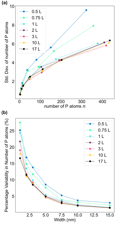
Finally, in Fig. 4a, we predict the relationship between the number of phosphorus atoms in a given APAM array, and the measured standard deviation in this number. We find a square root relationship in the error, supporting the intuition developed in Sec. 1 that multi-donor arrays can be qualitatively treated as a series of independent Bernoulli trials for a fixed probability of incorporation and a standard deviation . Since all of these simulations were done assuming perfect lithography, this relationship can be solely attributed to the stochastic nature of the phosphine decomposition pathway. The slope of the standard deviation curves varies as a function of the dose, which can then be related back to the probability of success in a Bernoulli trial via the formula for standard deviation. As the dose increases, the slope of the standard deviation curve stabilizes, indicating that the probability of incorporation saturates for doses greater than 1 L, matching intuition. These results indicate that the stochastic chemistry based error for a given APAM array will be a significant fraction of the total incorporated atoms at low system sizes such as single donor features, as shown in Fig. 4b. As the size of the APAM array increases, however, the error will saturate and become a much smaller fraction of total incorporations, making these large systems highly robust to the stochastic nature of phosphorus incorporation.
2.3 Impact of Lithographic Roughness
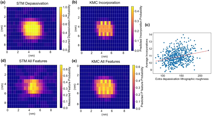
In a real world experiment, quite often the STM lithography will not be perfect, yielding windows with too many or (less often) too few sites depassivated. For example, note the varying shape and size of depassivated windows across the array in Fig. 1d. In Fig. 5a, we have averaged the actual depassivation rate for each dimer across 36 attempts at a 3 3 nm window using STM lithography. We calculate the image in Fig. 5a using thresholding to identify depassivated dimers, yielding a binary image followed by calculating mean of the set of 36 windows. Since depassivated dimers protrude from the surrounding passivated surface by a peak height of roughly 150 pm, we identify a dimer as depassivated if it’s median height exceeds a threshold value, chosen as 100 pm relative to the surrounding passivated surface. The fidelity of thresholding is comparable to more labor intensive visual-manual feature identification. In Fig. 5a, the soft transition from 0 to 1 over a range of about 1 nm in any direction indicates lithographic roughness that is typical in HDL. 19, 7, 20 While techniques such as feedback lithography could be used to improve the sharpness of the defined lithographic window 37, 38, this represents a reasonable STM lithography run that is similar to recent works utilized to fabricate quantum electronics. 19, 7, 20
Using our kinetic model, we predict that these errors in depassivation are often self-correcting, i.e. do not lead to significant deviations in the total number of incorporations for a given window. We investigate this by creating 500 depassivation patterns for our kinetic model based on the the empirical probability map in Fig. 5a. This approach assumes that the probability of depassivation at each dimer is independent, when in reality they are likely at least somewhat correlated. This model nevertheless serves as a good first approximation to real world systems, as any given configuration contains an average of up to 20 lattice sites depassivated that were not originally intended. In Fig. 5b, we demonstrate the predicted end location of incorporations, showing a sharp drop off in incorporations beyond the original window. While typical lithographic errors may be non-trivial beyond the intended window, these errors are largely self-correcting: the errors do not give the PH3 enough room to fully dissociate and thus are less likely to incorporate.
We further demonstrate the robustness of the incorporation to lithographic error by investigating the relationship between the “lithographic roughness” of a system and the number of incorporations. We define the total lithographic roughness for a given configuration as
| (1) |
where is a counter over the set of depassivation errors, and are the and locations of the error respectively, and and are the and locations of the nearest lattice site within the intended lithographic window. This definition of roughness means that in systems where depassivation errors occur close to the originally intended window, the score would be lower than in systems where the errors are far away from the intended window. As shown in Fig. 5c, we find a low correlation between the total lithographic roughness and the average number of incorporations for a system with an r2 value of just 0.06. While there is a slight positive correlation of incorporations with increased lithographic roughness, this variation is almost entirely swamped by the typical kinetic variation in total numbers of incorporations due to the uncertain chemical pathway for PH3 dissociation. We thus conclude that these atomic-precision processes in these systems are robust to typical lithographic error.
Finally, we demonstrate agreement between experiment and prediction in the location of post-doping incorporation-related features on the surface. Using STM data in Fig. 1e, acquired after dosing and annealing the lithographic windows used to generate the depassivation probability map in Fig. 5a, we threshold and count all features with height greater than 70 pm above the surrounding hydrogen passivation, then calculate a mean heatmap of P incorporation-related features in Fig. 5d. These features likely comprise a wide variety of features, including varying Si:P features and ejected Si adatoms on the surface. We identify all of these as likely to be P based features, not making strong distinctions between different PHx fragments, on the assumption that ejected Si adatoms represent P incorporating below this surface. This lack of distinction is both based on the limited resolution of the STM images and the desirability of developing a general sense of where P atoms are located on the surface, regardless of eventual incorporation. This is somewhat speculative; some amount of silicon adatoms will migrate both in and out of the window, and perhaps a few residual dangling bonds will be captured. Nevertheless, this provides a reasonable first-order estimate of where P features are located within a window. We then use our kinetic model to predict the location of all P atoms on the surface given an identical dosing and annealing process, as shown in Fig. 5e. The prediction matches the experimentally measured location well, with both showing peak probabilities in the center of the depassivated window around 60%. They both also show a steep dropoff in P features around the edge of the lithographic window, with only locations 1-2 lattice sites away from the intended window seeing significant levels of P buildup. In contrast to the predicted incorporations in Fig. 5b, however, the edge is less sharp, demonstrating that the need for PH3 dissociation is the main physical mechanism for atomic-precision in response to lithographic error. This provides a useful check on our kinetic model, giving confidence to our earlier predictions of the robustness of multi-donor incorporation.
3 Summary
Using kinetic simulations of the APAM doping process facilitated by hydrogen desorption lithography, we have predicted that multi-donor arrays are robust to both chemical and lithographic variation. Our results suggest that for small lithographic windows, even a window three silicon dimers wide and two dimer rows tall is sufficient to guarantee at least a single P incorporation. They also suggest that at window sizes larger than 5 nm the incorporation per unit area remains relatively constant, defining the scale at which edge effects become less pronounced. We further predict that the behavior of the system can, to a first order, be taken as a series of independent Bernoulli trials for each incorporation event. We examine typical lithographic variation in creating APAM windows, and simulations suggest that little correlation exists between the “roughness” of lithography and the resulting incorporations. This suggests that lithographic errors are largely self-correcting. Finally, we corroborate our model by comparing the predicted location of all PHx fragments on the surface to STM images.
Our results suggest that APAM multi-donor arrays are robust to typical sources of error in both lithographic and chemical processes. Thus APAM fabrication should be reliable for scalable device applications where more than a single donor can be used in individual elements (e.g., arrays of quantum dots).
We gratefully acknowledge useful conversations with Scott Schmucker, Rick Muller, Peter Schultz, and Joe Simonson. This work was partially supported by the Laboratory Directed Research and Development program at Sandia National Laboratories under project 213017 (FAIR DEAL) and project 226354. This work was also performed, in part, at the Center for Integrated Nanotechnologies, a U.S. DOE, Office of Basic Energy Sciences user facility. Sandia National Laboratories is a multi-mission laboratory managed and operated by National Technology and Engineering Solutions of Sandia, LLC, a wholly owned subsidiary of Honeywell International, Inc., for DOE’s National Nuclear Security Administration under contract DE-NA0003525. This paper describes objective technical results and analysis. Any subjective views or opinions that might be expressed in the paper do not necessarily represent the views of the U.S. Department of Energy or the United States Government.
Appendices are included in the Supporting Information concerning (A) DFT calculations across multiple silicon dimer rows, (B) Kinetic Monte Carlo details, and (C) 33 nm heatmaps of incorporation.
References
- Georgescu et al. 2014 Georgescu, I. M.; Ashhab, S.; Nori, F. Quantum simulation. Reviews of Modern Physics 2014, 86, 153
- Prati et al. 2012 Prati, E.; Hori, M.; Guagliardo, F.; Ferrari, G.; Shinada, T. Anderson–Mott transition in arrays of a few dopant atoms in a silicon transistor. Nature nanotechnology 2012, 7, 443
- Prati et al. 2016 Prati, E.; Kumagai, K.; Hori, M.; Shinada, T. Band transport across a chain of dopant sites in silicon over micron distances and high temperatures. Scientific reports 2016, 6, 19704
- Le et al. 2017 Le, N. H.; Fisher, A. J.; Ginossar, E. Extended Hubbard model for mesoscopic transport in donor arrays in silicon. Physical Review B 2017, 96, 245406
- Dusko et al. 2018 Dusko, A.; Delgado, A.; Saraiva, A.; Koiller, B. Adequacy of Si:P chains as Fermi–Hubbard simulators. npj Quantum Information 2018, 4, 1–5
- Altman et al. 2021 Altman, E.; Brown, K. R.; Carleo, G.; Carr, L. D.; Demler, E.; Chin, C.; DeMarco, B.; Economou, S. E.; Eriksson, M. A.; Fu, K.-M. C., et al. Quantum Simulators: Architectures and Opportunities. PRX Quantum 2021, 2, 017003
- Wang et al. 2021 Wang, X.; Khatami, E.; Fei, F.; Wyrick, J.; Namboodiri, P.; Kashid, R.; Rigosi, A. F.; Bryant, G.; Silver, R. Quantum Simulation of an Extended Fermi-Hubbard Model Using a 2D Lattice of Dopant-based Quantum Dots. arXiv preprint arXiv:2110.08982 2021,
- Büch et al. 2013 Büch, H.; Mahapatra, S.; Rahman, R.; Morello, A.; Simmons, M. Spin readout and addressability of phosphorus-donor clusters in silicon. Nature Communications 2013, 4, 1–6
- Hill et al. 2015 Hill, C. D.; Peretz, E.; Hile, S. J.; House, M. G.; Fuechsle, M.; Rogge, S.; Simmons, M. Y.; Hollenberg, L. C. A surface code quantum computer in silicon. Science Advances 2015, 1, e1500707
- Pakkiam et al. 2018 Pakkiam, P.; House, M. G.; Koch, M.; Simmons, M. Y. Characterization of a scalable donor-based singlet–triplet qubit architecture in silicon. Nano letters 2018, 18, 4081–4085
- Pakkiam et al. 2018 Pakkiam, P.; Timofeev, A.; House, M.; Hogg, M.; Kobayashi, T.; Koch, M.; Rogge, S.; Simmons, M. Y. Single-shot single-gate rf spin readout in silicon. Physical Review X 2018, 8, 041032
- He et al. 2019 He, Y.; Gorman, S.; Keith, D.; Kranz, L.; Keizer, J.; Simmons, M. A two-qubit gate between phosphorus donor electrons in silicon. Nature 2019, 571, 371–375
- Koch et al. 2019 Koch, M.; Keizer, J. G.; Pakkiam, P.; Keith, D.; House, M. G.; Peretz, E.; Simmons, M. Y. Spin read-out in atomic qubits in an all-epitaxial three-dimensional transistor. Nature Nanotechnology 2019, 14, 137–140
- Bussmann et al. 2021 Bussmann, E.; Butera, R. E.; Owen, J. H.; Randall, J. N.; Rinaldi, S. M.; Baczewski, A. D.; Misra, S. Atomic-precision advanced manufacturing for Si quantum computing. MRS Bulletin 2021, 46, 607–615
- Škereň et al. 2018 Škereň, T.; Pascher, N.; Garnier, A.; Reynaud, P.; Rolland, E.; Thuaire, A.; Widmer, D.; Jehl, X.; Fuhrer, A. CMOS platform for atomic-scale device fabrication. Nanotechnology 2018, 29, 435302
- Ward et al. 2020 Ward, D. R.; Schmucker, S. W.; Anderson, E. M.; Bussmann, E.; Tracy, L.; Lu, T.-M.; Maurer, L. N.; Baczewski, A.; Campbell, D. M.; Marshall, M. T.; Misra, S. Atomic Precision Advanced Manufacturing for Digital Electronics. Electronic Device Failure Analysis 2020, 22, 4–11
- Schofield et al. 2003 Schofield, S. R.; Curson, N. J.; Simmons, M. Y.; Rueß, F. J.; Hallam, T.; Oberbeck, L.; Clark, R. G. Atomically precise placement of single dopants in Si. Physical Review Letters 2003, 91, 136104
- Füchsle et al. 2010 Füchsle, M.; Mahapatra, S.; Zwanenburg, F.; Friesen, M.; Eriksson, M.; Simmons, M. Y. Spectroscopy of few-electron single-crystal silicon quantum dots. Nature Nanotechnology 2010, 5, 502–505
- Wyrick et al. 2019 Wyrick, J.; Wang, X.; Kashid, R. V.; Namboodiri, P.; Schmucker, S. W.; Hagmann, J. A.; Liu, K.; Stewart Jr, M. D.; Richter, C. A.; Bryant, G. W., et al. Atom-by-atom fabrication of single and few dopant quantum devices. Advanced Functional Materials 2019, 29, 1903475
- Kiczysnski et al. 2022 Kiczysnski, M.; Gorman, S. K.; Geng, H.; Donnelly, M. B.; Chung, Y.; He, Y.; Keizer, J. G.; Simmons, M. Y. Engineering topological states in atom-based semiconductor quantum dots. Nature 2022, 606, 694–699
- Ivie et al. 2021 Ivie, J. A.; Campbell, Q.; Koepke, J. C.; Brickson, M. I.; Schultz, P. A.; Muller, R. P.; Mounce, A. M.; Ward, D. R.; Carroll, M. S.; Bussmann, E., et al. Impact of incorporation kinetics on device fabrication with atomic precision. Physical Review Applied 2021, 16, 054037
- Warschkow et al. 2016 Warschkow, O.; Curson, N.; Schofield, S.; Marks, N.; Wilson, H.; Radny, M.; Smith, P.; Reusch, T.; McKenzie, D.; Simmons, M. Y. Reaction paths of phosphine dissociation on silicon (001). The Journal of Chemical Physics 2016, 144, 014705
- 23 Kinetic Monte Carlo code. https://github.com/quantumquinn/apam-kmc
- Fuechsle et al. 2012 Fuechsle, M.; Miwa, J. A.; Mahapatra, S.; Ryu, H.; Lee, S.; Warschkow, O.; Hollenberg, L. C.; Klimeck, G.; Simmons, M. Y. A single-atom transistor. Nature Nanotechnology 2012, 7, 242–246
- Füchsle 2011 Füchsle, M. Precision Few-Electron Silicon Quantum Dots. Ph.D. thesis, 2011
- Wyrick et al. 2021 Wyrick, J.; Wang, X.; Namboodiri, P.; Kashid, R. V.; Fei, F.; Fox, J.; Silver, R. M. Enhanced Atomic Precision Fabrication by Adsorption of Phosphine into Engineered Dangling Bonds on H-Si Using Scanning Tunneling Microscopy and Density Functional Theory. arXiv preprint arXiv:2112.12200 2021,
- Campbell et al. 2021 Campbell, Q.; Ivie, J. A.; Bussmann, E.; Schmucker, S. W.; Baczewski, A. D.; Misra, S. A Model for Atomic Precision p-Type Doping with Diborane on Si(100)-21. The Journal of Physical Chemistry C 2021, 125, 481–488
- Campbell et al. 2022 Campbell, Q.; Dwyer, K. J.; Baek, S.; Baczewski, A. D.; Butera, R. E.; Misra, S. Reaction pathways of BCl3 for acceptor delta-doping of silicon. arXiv preprint arXiv:2201.11682 2022,
- Yu et al. 1986 Yu, M. L.; Vitkavage, D.; Meyerson, B. Doping reaction of PH3 and B2H6 with Si (100). Journal of applied physics 1986, 59, 4032–4037
- Lin et al. 1999 Lin, D.-S.; Ku, T.-S.; Sheu, T.-J. Thermal reactions of phosphine with Si (100): a combined photoemission and scanning-tunneling-microscopy study. Surface science 1999, 424, 7–18
- Schofield et al. 2006 Schofield, S. R.; Curson, N. J.; Warschkow, O.; Marks, N. A.; Wilson, H. F.; Simmons, M. Y.; Smith, P. V.; Radny, M. W.; McKenzie, D. R.; Clark, R. G. Phosphine dissociation and diffusion on Si (001) observed at the atomic scale. The Journal of Physical Chemistry B 2006, 110, 3173–3179
- Wang et al. 1994 Wang, Y.; Chen, X.; Hamers, R. J. Atomic-resolution study of overlayer formation and interfacial mixing in the interaction of phosphorus with Si (001). Physical Review B 1994, 50, 4534
- Shen et al. 2002 Shen, T.-C.; Ji, J.-Y.; Zudov, M.; Du, R.-R.; Kline, J.; Tucker, J. Ultradense phosphorous delta layers grown into silicon from PH 3 molecular precursors. Applied Physics Letters 2002, 80, 1580–1582
- Oberbeck et al. 2002 Oberbeck, L.; Curson, N.; Simmons, M.; Brenner, R.; Hamilton, A.; Schofield, S.; Clark, R. Encapsulation of phosphorus dopants in silicon for the fabrication of a quantum computer. Applied physics letters 2002, 81, 3197–3199
- McKibbin et al. 2009 McKibbin, S.; Clarke, W.; Fuhrer, A.; Reusch, T.; Simmons, M. Investigating the regrowth surface of Si: P -layers toward vertically stacked three dimensional devices. Applied Physics Letters 2009, 95, 233111
- McKibbin et al. 2014 McKibbin, S.; Polley, C.; Scappucci, G.; Keizer, J.; Simmons, M. Low resistivity, super-saturation phosphorus-in-silicon monolayer doping. Applied Physics Letters 2014, 104, 123502
- Hersam et al. 2000 Hersam, M.; Guisinger, N.; Lyding, J. Silicon-based molecular nanotechnology. Nanotechnology 2000, 11, 70
- Wyrick et al. 2018 Wyrick, J.; Wang, X.; Namboodiri, P.; Schmucker, S. W.; Kashid, R. V.; Silver, R. M. Atom-by-atom construction of a cyclic artificial molecule in silicon. Nano letters 2018, 18, 7502–7508
- Giannozzi et al. 2009 Giannozzi, P.; Baroni, S.; Bonini, N.; Calandra, M.; Car, R.; Cavazzoni, C.; Ceresoli, D.; Chiarotti, G. L.; Cococcioni, M.; Dabo, I., et al. QUANTUM ESPRESSO: a modular and open-source software project for quantum simulations of materials. Journal of physics: Condensed matter 2009, 21, 395502
- van Setten et al. 2018 van Setten, M. J.; Giantomassi, M.; Bousquet, E.; Verstraete, M. J.; Hamann, D. R.; Gonze, X.; Rignanese, G.-M. The PseudoDojo: Training and grading a 85 element optimized norm-conserving pseudopotential table. Computer Physics Communications 2018, 226, 39–54
- Perdew et al. 1996 Perdew, J. P.; Burke, K.; Ernzerhof, M. Generalized gradient approximation made simple. Physical review letters 1996, 77, 3865
- Monkhorst and Pack 1976 Monkhorst, H. J.; Pack, J. D. Special points for Brillouin-zone integrations. Physical review B 1976, 13, 5188
- Bortz et al. 1975 Bortz, A.; Kalos, M.; Lebowitz, J. A New Algorithm for Monte Carlo Simulation of Ising Spin Systems. Journal of Computational physics 1975, 17, 10–18
- Gillespie 1976 Gillespie, D. T. A general method for numerically simulating the stochastic time evolution of coupled chemical reactions. Journal of Computational Physics 1976, 22, 403–434
- Leetmaa and Skorodumova 2014 Leetmaa, M.; Skorodumova, N. V. KMCLib: A general framework for lattice kinetic Monte Carlo (KMC) simulations. Computer Physics Communications 2014, 185, 2340–2349
- Arrhenius 1889 Arrhenius, S. Über die Reaktionsgeschwindigkeit bei der Inversion von Rohrzucker durch Säuren. Zeitschrift für physikalische Chemie 1889, 4, 226–248
Appendix A: DFT calculations across multiple silicon dimer rows
1 Electronic Structure Calculation Details
All total energy calculations are performed using the plane wave quantum-espresso software package.39 To compute reaction barriers between configurations we use the Nudged Elastic Band (NEB) method, also implemented in quantum-espresso. We use norm-conserving pseudopotentials from the PseudoDojo repository 40 and the Perdew-Burke-Ernzerhof exchange correlation functional. 41 We use kinetic energy cutoffs of 50 Ry and 200 Ry for the plane wave basis sets used to describe the Kohn-Sham orbitals and charge density, respectively. We use a 221 Monkhorst-Pack grid to sample the Brillioun zone.42
We perform all adsorption energy calculations on the 44 supercell of a seven-layer thick Si(100)-21 slab with a 20 Å vacuum region, where a single unit cell has a size of 3.87 Å3.87 Å. Matching the experimentally measured silicon structure, we model the silicon surface as antisymmetric with alternating buckled silicon dimers. On the other end of the slab, the dangling bonds of the silicon are passivated with selenium atoms to prevent spurious surface effects. Selenium was determined to be optimal for achieving this purpose with minimal strain. The bottom four layers of the slab are frozen and the geometry of the surface layers along with the adsorbate are relaxed until the interatomic forces are lower than 50 meV/Å.
2 Reaction barriers of reactions across multiple silicon dimers
We use Density Functional Theory (DFT) calculations to predict the reaction barriers of various reactions taking place across dimers. Given the distance between silicon dimer rows in the (100)-21 reconstruction is only 3.5 Å, reactions across these rows are not only possible, but likely. While Warschkow et al. explored some of these reactions (corresponding to Fig. A1b),22 we present a comprehensive report of these reactions and their reaction barriers in Fig. A1 and Fig. A2, which we apply in the kinetic model used throughout this work. We investigate PH3 and PH2 fragments either shedding hydrogen to the neighboring dimer row, or fully migrating on its own. We also simultaneously examine the same reaction when the neighboring dimer row is partially occupied, which leads to a uniform decrease of the reaction barrier.
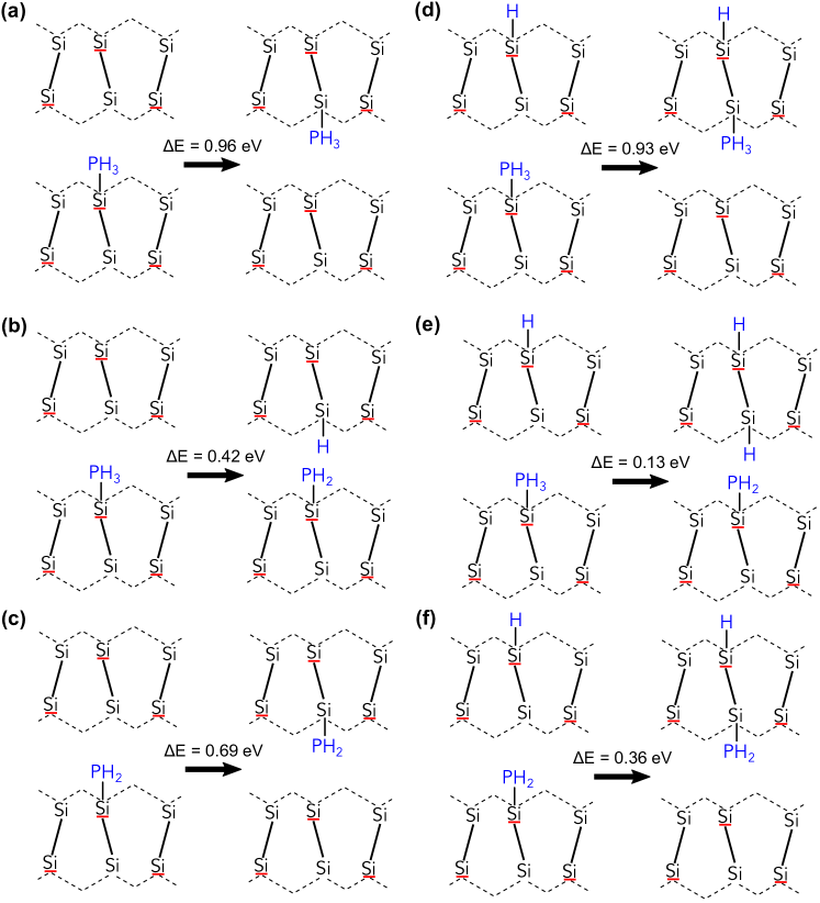
Most notably, the barrier for the reaction shown in Fig. A1b shows that a freshly adsorbed PH3 losing its hydrogen across dimer rows has nearly the same barrier (0.42 eV) as losing within the same dimer row (0.46 eV). This will lead to a significant spread of hydrogen across dimer rows as opposed to previous models where only reactions along the same dimer row are allowed. We also find that the barrier for a PH2 fragment jumping ship and moving to the neighboring silicon dimer row (0.69 eV) is only slightly higher than migration along the same dimer row (0.58 eV as predicted by Warschkow et al.), making migration of the phosphorus atom itself to a different dimer row a small but distinct possibility. In general, our calculations show that reactions that take place across multiple silicon dimer rows cannot be neglected in realistic models of multi-row patches.
Appendix B: Kinetic Monte Carlo Details
We use a Kinetic Monte Carlo model 43, 44 as implemented in the KMClib package 45 to determine the probability of incorporation. Our KMC model uses transition rates based on the Arrhenius equation 46, where is transition rate, is the attempt frequency, is the reaction barrier found from our earlier DFT calculations, is the Boltzmann constant, and is the temperature. We set all attempt frequencies to s-1 as a reasonable order of magnitude estimate based on an analysis of attempt frequencies for the dissociation of phosphine on silicon 22. We calculate the effusive flow rate of molecules landing on any particular silicon dimer as , where is the pressure of the incoming precursor gas, is the area of impingement, taken here as a single silicon dimer, is the mass of the precursor gas.
Each KMC calculation is repeated 200 times with different random seeds, and the sample mean of the results is reported. We calculate error bars by assuming a binomial distribution of measured counts and using the standard error based on sample size.
Appendix C: 3 3 nm heatmaps of incorporation
We next expand our kinetic model to investigate larger windows to examine the spatial distribution of incorporation for wider -doped regions. In Fig. C1, we predict the spatial distribution of a 3 nm 3 nm wide region which has been -doped. As noted in Sec. LABEL:sec:proxy-choice, the choice within our model of which molecule to use as a proxy for eventual incorporation can lead to significant differences in both the level and position of incorporation events.
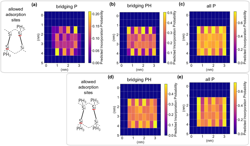
In Fig C1a, we use a bridging PH molecule as our proxy for incorporation. The most striking feature of the incorporation map here is the difference between the top and bottom dimer rows and the dimer rows in the middle of the structure. The top and bottom dimer rows both exhibit a checkerboard pattern, with every other silicon dimer having significant levels of incorporation, while the other sites see dramatically lowered levels of incorporation. This pattern can ultimately be attributed to the combination of the cross-dimer reaction illustrated in Fig. A1b, and the alternating tilt of silicon dimers. In the reconstructed silicon (100)-21 surface, each atom of a silicon dimer either tilts up or down and the silicon dimer next to it will have the opposite arrangement of tilts. Furthermore it is more favorable for a phosphine atom to adsorb on the lower end of the dimer, and within our model, we only allow this adsorption process, and not one at the higher end. This becomes important due to the low reaction barrier of a hydrogen dissociating from a PH3 on one dimer row to land on the silicon atom of the nearby separate dimer row. In our model, this is the lowest reaction barrier for a PH3 PH2 + H reaction, and thus highly favored. On the top and bottom rows, however, this means that it is only easy for half of the PH3 molecules to dissociate: the half which have an open silicon dimer row next to it and are not site blocked by the hydrogen termination of the pattern. These PH2 fragments go on to dissociate with high favorability and the shedded hydrogen further invade the nearby silicon dimers and block many dissociation pathway for these adsorbed PH3 molecules. In the middle of the depassivated window, the phosphine can dissociate to neighboring dimer rows on either side, and thus the checkerboard effect of the alternating up-down tilt on incorporation is not observed.
While this pattern produces a striking predictions, it should be noted that while it is more favorable for a phosphine atom to adsorb on the lower end of a silicon dimer, it is still favorable on the upper end and likely to occur. Within our model, we have assumed that phosphine molecules will always adsorb at this lower end, but in reality this preference is less strong. This, plus the tendency of dimer tilts to rapidly flip on the silicon surface, would likely lead to this checkerboard trend being, at best, dimly observed in real world devices. We verify this by also simulating systems where phosphine is allowed to adsorb on all silicon atoms with results shown in Fig. C1d and e. We indeed note that the checkerboard pattern is less well pronounced, although the predicted incorporation levels do not alter significantly.