Indirect band gap semiconductors for thin-film photovoltaics: High-throughput calculation of phonon-assisted absorption
Abstract
Discovery of high-performance materials remains one of the most active areas in photovoltaics (PV) research. Indirect band gap materials form the largest part of the semiconductor chemical space, but predicting their suitability for PV applications from first principles calculations remains challenging. Here we propose a computationally efficient method to account for phonon assisted absorption across the indirect band gap and use it to screen 127 experimentally known binary semiconductors for their potential as thin film PV absorbers. Using screening descriptors for absorption, carrier transport, and nonradiative recombination, we identify 28 potential candidate materials. The list, which contains 20 indirect band gap semiconductors, comprises both well established (3), emerging (16), and previously unexplored (9) absorber materials. Most of the new compounds are anion rich chalcogenides (TiS3, Ga2Te5) and phosphides (PdP2, CdP4, MgP4, BaP3) containing homoelemental bonds, and represent a new frontier in PV materials research. Our work highlights the previously underexplored potential of indirect band gap materials for optoelectronic thin-film technologies.
I. Introduction
Renewable electricity produced by photovoltaics (PV) is likely to become a cornerstone of a future sustainable and climate-neutral energy system. Although the current PV technology is mainly based on silicon (Si) wafer solar cells (26.7 efficiency)Green et al. (2022); Yoshikawa et al. (2017), thin film technologies have distinct advantages such as mechanical flexibility, reduced material usage, potential for low-cost, low-temperature processing, and integration with existing Si technology in tandem solar cells. After decades of research and device optimization various thin film absorber materials, like GaAs (29.1), CdTe (22.1), InP (24.2), CIGS (23.4), etc.Wanlass (2017); Green and Ho-Baillie (2019); Nakamura et al. (2019); Green et al. (2022) have reached efficiencies comparable to the Si-based technology. Most recently, hybrid lead-halide perovskite (MAPbI3) has emerged as an additional PV candidate material with a record efficiency of 25.8 Min et al. (2021).
Although promising, the thin film PV materials still suffer from major drawbacks associated with low material abundance (In, Ga), toxicity (Cd, As, Pb), and long-term device stability under ambient conditions (hybrid perovskites), which hinder their large-scale deployment. As such, the discovery of new (thin-film) PV materials remains a relevant and timely challenge. Within the PV literature, the most widely used selection-metric for absorber materials is the electronic band gap. Indeed, Shockley and Queisser demonstrated that thermodynamic detailed balance sets an upper limit to the power conversion efficiency (PCE) of a semiconductor given solely by its band gap.Shockley and Queisser (1961) More realistic PV descriptors have been developed by invoking further physical properties like the optical absorption coefficient, the carrier mobility, and internal quantum efficiency, along with device related aspects such as film thickness, light-trapping schemes, etc.Tiedje et al. (1984); Yu and Zunger (2012); Blank et al. (2017); Kim et al. (2020)
Recently, the substantial increase in computer power along with improvements in theoretical methods have ushered in an era where it is possible to screen for new materials faster, cheaper, and more rationally than the traditional approach based on experimental trial and error. In particular, high-throughput density functional theory (DFT) calculations have been employed to identify suitable PV candidate materials.Zhao et al. (2017); Kuhar et al. (2018); Choudhary et al. (2019); Li and Yang (2019); Luo et al. (2021); Dahliah et al. (2021); Gan et al. (2022) Indirect band gap semiconductors, which occupy a major portion of the semiconductor space, have mostly been ignored in these studies. This is because indirect gap materials will absorb photons less efficiently around the band gap, which is likely to lead to low PCE in thin film devices. On the other hand, it has been argued that a small indirect gap might be beneficial for PV applications due to reduced radiative recombination.Hutter et al. (2017); Kirchartz and Rau (2017) This situation clearly calls for a clarification.
The major bottleneck in evaluating the PV performance of an indirect band gap semiconductor from first-principles, is modeling indirect absorption. This is a higher order process involving one or several phonons (or defects or free carriers) in addition to the photon. Such calculations are very demanding. As a consequence, ab-initio calculations of momentum-indirect absorption has so far been limited to a few materialsNoffsinger et al. (2012); Kang et al. (2018); Monserrat et al. (2018); Menéndez et al. (2018); Bravić and Monserrat (2019); Ha et al. (2020); Ge et al. (2020); Jian et al. (2021); Willis et al. (2022).
In this work, we propose an approximate method to evaluate phonon-assisted absorption in indirect band gap semiconductors, which only involves the -point optical phonons and therefore is feasible for high-throughput studies. After establishing the accuracy of the approach for a few prototypical materials, we use it to evaluate the key PV performance parameters for 127 stable, binary semiconductors of which 97 have indirect band gaps. In addition to already known materials, we identify a number of new indirect band gap materials that show promising potential for thin film PV. All the materials along with their calculated properties are available in an open online database. To the best of our knowledge, this is the first high-throughput study evaluating indirect gap materials for PV, which includes calculation of phonon-assisted absorption.
II. Method
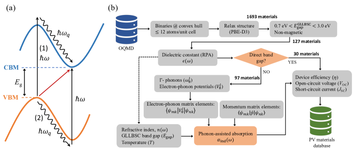
Phonon assisted absorption is a second order process, which involves a photon-phonon pair satisfying (crystal) momentum conservation (see Fig.1(a)). Because of the involved sum over intermediate states and the need to calculate all the phonons and electron-phonon couplings, its calculation from first-principles is very demanding. In this work we use a simplified approach that involves only the optical -point phonons. Within second order perturbation theory, the phonon-assisted absorption is given by,
| (1) |
where,
| (2) |
Here is the energy of the incident photon, denotes the phonon mode and its momentum, and is the refractive index of the semiconductor. The two sums in the square bracket of Eq. (2) correspond to the two transition pathways denoted ’1’ and ’2’ in Fig.1(a). The matrix elements appearing in Eq. (2) contain the electron-phonon potential, , and coupling to a photon field of polarisation , respectively. The phonon occupation factors, , are given by the Bose-Einstein distribution.
In our approximation, we assume that scattering on a -phonon can be replaced by scattering on a -phonon (acoustic phonons are disregarded). Specifically, we keep all transitions in Eq. (2), but make the replacements
| (3) | |||||
| (4) |
where is the periodic part of the Bloch function. Our approximation avoids the computation of the full -dependent phonons and electron-phonon couplings and instead requires these quantities only at the -point. The efficiency gain is largest for materials with small unit cells and it becomes exact in the limit of a large unit cell. In particular, due to band folding, the exact result for any crystal is obtained by using a supercell containing a sufficiently large number of copies of the primitive cell (although this strategy is inefficient as momentum selection rules are not exploited). Below we illustrate the performance of our approach for the case of bulk silicon, and refer to the supplementary information (SI) for further tests (BP, MoS2, MoSe2, etc.), all showing encouraging results. Details of the DFT calculations can be found in section V. Methodology.
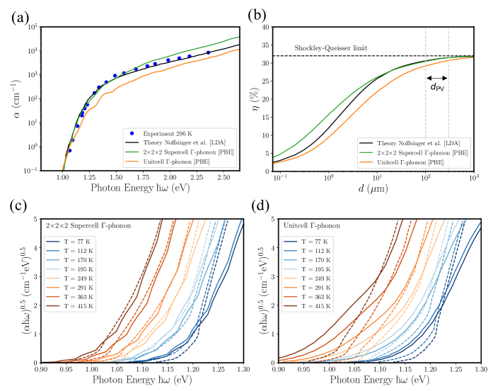
Fig. 2(a) shows the phonon-assisted absorption in silicon obtained within our approximate scheme applied to the Si primitive unit cell (orange - 3 optical phonons included) and a supercell containing repetitions of the primitive cell (green - 45 optical phonons). Our results are compared to experimental data (K) and a previous ab-initio result including all phonons. The theoretical spectra have been shifted horisontally to match the experimental absorption onset. We have checked that the use of the LDA and PBE xc-functionals lead to insignificant changes in the spectrum. While our supercell -phonon approach shows excellent agreement with both sets of reference data, the primitive unit cell -phonon approach slightly underestimates the absorption coefficient. Next, we add the first order absorption coefficient, , (calculated in the random phase approximation (RPA)) to the indirect absorption coefficients and evaluate the radiative device PCE, , as a function of thickness of the Si absorber, see Fig. 2(b). Overall, the different descriptions of the indirect absorption leads to similar PCEs with the most approximate -phonon description underestimating the PCE by maximum relative to experiments. The last two panels of Fig. 2 show the temperature dependence of the indirect absorption as calculated with the -phonons of the supercell (c) and primitive cell (d), respectively. The supercell calculations are in excellent agreement with the experimental data (dashed lines), except for small deviations at temperatures below 100K. The primitive cell calculations show larger deviations – also at higher close to the absorption onset.
The workflow used to calculate the PV performance parameters is illustrated in Fig. 1(b). For 1693 thermodynamically stable elemental and binary compounds from the Open Quantum Materials Database (OQMD) with up to 12 atoms/unit cell, we perform structural relaxations using the PBEPerdew et al. (1996) xc-functional with D3 correctionsGrimme et al. (2010) to account for van der Waals interactions (more details can be found in computational details section). The data set includes 338 semiconductorsSvendsen et al. (2022) for which we evaluate the band gaps using both the PBE and the GLLBSCKuisma et al. (2010) xc-functional. Keeping only nonmagnetic compounds with GLLBSC band gap between 0.7 eV and 3.0 eV, reduces the data set further down to 127 compounds. For these materials, the complex dielectric function is calculated in the RPA (this is a first order response function including only direct momentum-conserving transitions with local field effects accounted for). For the 97 semiconductors with indirect band gap, the phonon assisted absorption coefficient is calculated using the -phonon approximation in the primitive unit cell, c.f. Eqs. (1-2). Finally, the PV parameters are evaluated from the total absorption coefficient, including first and second order processes, as described in SI in section S1.
III. Results and discussion
A. Descriptors
The main descriptor used to quantify the potential of a PV absorber material, is its power conversion efficiency (PCE), , which can be expressed as,
| (5) |
In this expression is the voltage, is the short-circuit current density, is total recombination current density, and is the temperature. In the denominator, we have the input power density, where represents the photon flux from the incident solar spectrum (we have used the standard AM1.5G solar spectrum). More details can be found in Methodology section in SI. Here we stress that the only input required to obtain from Eq. (5) in the radiative limit (i.e. when non-radiative recombination processes are neglected and thus internal quantum efficiency ) is the material’s absorption spectrum.
In the simplest theory, the absorbance is assumed to be zero below the band gap and one above. In the radiative limit this yields the well known Shockley-Queisser (SQ) limit.Shockley and Queisser (1961) Clearly, this description fails to differentiate between different materials with the same band gap. While this is a reasonable approximation for bulk cells, a realistic description of thin film devices must account for the finite thickness and frequency dependent absorption.Tiedje et al. (1984); Yu and Zunger (2012); Blank et al. (2017)
A popular PV performance descriptor that invokes the absorption coefficient is the Spectroscopic Limited Maximum Efficiency (SLME).Yu and Zunger (2012) The SLME sets in Eq. (5) to account for non-radiative recombination. In other words, the effect of an indirect band gap is taken into account via an increased non-radiative loss rate. In fact, this can lead to erroneous conclusions for indirect band gap materials. For example, the calculated SLME for Si at 100 m thickness is only 1, while the experimental PCE is around 25%. We argue that explicitly accounting for indirect absorption processes is essential for a proper description of PV performance parameters across all band gap types. In particular, given the exact absorption coefficient, Eq. (5) would yield the exact PCE in the radiative limit. More detailed discussion is provided in the SI section S3. To account for non-radiative recombination we use the formalism proposed by Blank et al.Blank et al. (2017) as discussed later.
B. Si as a case study
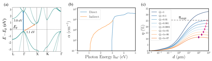
Before discussing our high-throughput results, we illustrate the PV analysis in detail for the well known case of Si. The silicon crystal has an indirect band gap of 1.1 eV, whereas the direct band gap at the -point is 3.0 eV (see Fig. 3(a)). Since the first-order absorption coefficient (e.g. evaluated using the independent particle approximation, the RPA, or the Bethe-Salpeter Equation), only includes vertical transitions, it will fail to account for photon absorption below the direct gap. The effect of including phonon-assisted transitions in the absorption coefficient can be seen in Fig. 3(b) (the orange curve is the same as shown in Fig. 2(a)). While the second-order processes are weak, they are completely essential for a correct description of the opto-electronic properties. In the radiative limit we obtain a PCE of 31.3% (with phonon-assisted processes) and 4.9% (only first-order processes) for a 100 m thick Si film.
To move beyond the radiative approximation one must account for non-radiative recombination such as Shockley-Read-Hall recombinationShockley and Read Jr (1952); Hall (1952) and Auger processesHuldt (1971). These are challenging to evaluate from first principles and to some extent dependent on the sample quality via the concentration and types of defects in the material. In addition, there are additional loss channels that depend on the device architecture, such as surface and interface recombination. Here we will neglect the latter types, and only consider the non-radiative processes taking place within the absorbing layer. To that end, we follow Blank et al.Blank et al. (2017) who proposed a detailed balance compatible approach where non-radiative processes are included via the internal luminescence quantum efficiency, (the ratio of the radiative to the total recombination rates inside the material under equilibrium conditions), which becomes a free parameter, see Section S1 in SI for more details.
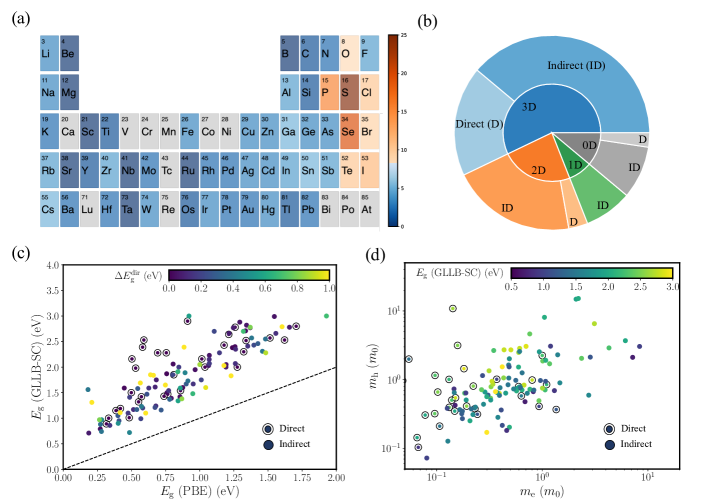
Fig. 3(c) shows the calculated vs film thickness for different values of . As expected, with increasing non-radiative recombination the maximum achievable efficiency decreases. Perhaps less obvious, also the optimal thickness (thickness at which is maximum) decreases when the non-raditaive recombination increases. This effect occurs because the optimal thickness occurs exactly when the increase in absorption due to a further increase in thickness is balanced by the increase in the non-radiative recombination. The existence of an optimal thickness then follows by noting that the former decays exponentially through the material while the latter is constant. We obtain an efficiency close to the experimental value () of 25 at optimal film thickness for around , see Fig. 3(c). The experimental value of in the highest-efficiency Si solar cell Yoshikawa et al. (2017) is Green and Ho-Baillie (2019), which implies a maximum efficiency of about 23%. We ascribe this small underestimation of the PCE to the -point phonon approximation and to the fact that the front surface of a real Si solar cell is textured to promote light scattering and increase the average optical path of photons in Si. Both approximations lead to a slight underestimation of the fraction of incident light absorbed in a film of given thickness, see Fig. 2(b).
C. High-throughput screening
Moving on to the main purpose of our work, namely the identification of high-performance indirect band gap PV absorbers, Fig. 4(a) shows the distribution of chemical elements in the 127 semiconductors that were subject to the workflow in Fig. 1(b). There is a relatively homogeneous distribution of cations, with the exception of certain 3d transition metals, which are absent because we have excluded magnetic materials. The anionic elements are dominated by the chalcogens (in particular sulphur) followed by the halogens. We note that we did not filter out materials containing rare or toxic elements at this step. In Fig. 4(b) we show how the 127 compounds are distributed over the dimensionality of their covalently bonded atomic clusters. The dimensionality analysis follows the method of Larsen et al.Larsen et al. (2019). It can be seen that the materials are almost evenly divided between ’3D’ and ’non-3D’ materials. About 50% of the latter class are van der Waals (vdW) layered 2D materials while the remainder are vdW-bonded 1D or 0D clusters. For each dimensionality class we show the fraction of direct (D) and indirect (ID) band gaps.
In total, more than 75 of the 127 semiconductors possess an indirect band gap. Fig. 4(c) shows the band gap distribution for our dataset. It is well known that the PBE xc-functional systematically underestimates the band gap. The GLLB-SC functional provides more accurate band gaps at little extra computational costKuisma et al. (2010); Rasmussen and Thygesen (2015). An important reason behind the good performance of the GLLB-SC is includes a correction of the Kohn-Sham band gap to account for the so-called derivative discontinuity. The GLLB-SC band gaps range from 0.7 eV to 3.0 eV, whereas with PBE band gap lies between 0.2 eV and 2 eV. From the color scale it is clear that most of the indirect gap materials have 0.5 eV while a only few compounds have 1.0 eV (all materials with above 1 eV have yellow color code) .
High absorption and low non-radiative recombination rates do not guarantee good PV performance. As an additional criterion, the carrier mobility, , should be high enough to ensure efficient electron-hole separation and extraction of charges at the contacts. The relaxation time, , accounts for scattering on other charge carriers, phonons, and crystal imperfections. While it can be accurately estimated from first principlesKaasbjerg et al. (2012); Kaasbjerg (2020), its calculation remains challenging in high-throughput studies. As a consequence we focus on the carrier effective mass
| (6) |
where is the effective mass along direction , which we calculate by fitting a parabola to the band extrema. Fig. 4(d) gives an overview of the hole and electron effective masses in the 127 semiconductors considered. The band gap is indicated by the color code.
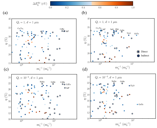
To evaluate the potential of a given PV material taking both optical absorption and carrier transport into account, we plot in Fig. 5 the PCE (for film thickness = 1 ) against the inverse carrier effective mass of electrons (left) and holes (right). We label all materials that are ”Pareto optimal”Khoroshiltseva et al. (2016), i.e. for which no other material has higher values for both and . In the upper panels (a-b), is evaluated in the radiative limit, , while we use a more realistic value of in the lower panels. The color scale represents the difference in direct and indirect band gap, .
Some well known thin film PV materials, like CdTe, PbS and InP, as well as emerging materials, like GaSe, SnS are found on the Pareto fronts in Fig. 5. Not unexpectedly, most of the promising PV materials have 0.5 eV (blueish rather than reddish color). In Table I, we list all materials satisfying the criteria: 20% at = 1, = 1 m, = 298 K, and , . The materials are ordered according to the size of . While there is a tendency for smaller to correlate with higher , there are also clear deviations from this trend. For example, SnSe2 with eV has , which is not far from the highest value obtained for the direct band gap material InP.
Established
Formula
space group
dim
(eV)
(m0)
(m0)
(%)
(%)
ICSD-id
InP
F-43m
3D
1.32
0.00
0.05
0.89
33.07
20.45
41443
CdTe
F-43m
3D
1.43
0.00
0.05
0.97
32.96
21.59
31844
PbS
Fm-3m
0D
1.15
0.00
0.24
0.31
32.86
17.99
62192
Emerging, PCE 5%
Formula
space group
dim
(eV)
(m0)
(m0)
(%)
(%)
ICSD-id
InSe
P63/mmc
2D
0.89
0.00
0.07
0.10
28.60
11.63
30377
Cu2O
Pn-3m
3D
1.01
0.00
0.93
0.41
30.52
14.89
261853
Se
P3121
1D
1.24
0.12
0.17
0.32
32.51
19.51
164271
WSe2
P63/mmc
2D
1.48
0.66
0.47
0.84
26.80
18.74
40752
Emerging, PCE 5%
Formula
space group
dim
(eV)
(m0)
(m0)
(%)
(%)
ICSD-id
GaSe
P63/mmc
2D
1.47
0.00
0.11
0.21
32.34
21.78
41978
ZnTe
P31
3D
2.00
0.00
0.08
0.31
22.98
17.53
80076
Ga2Se3
Cc
3D
2.00
0.00
0.15
0.35
22.88
17.56
35028
GeSe
Pnma
2D
1.60
0.03
0.23
0.40
30.00
20.93
17006
SnS
Pnma
2D
1.39
0.06
0.21
0.37
33.03
21.27
24376
InI
Cmcm
0D
2.00
0.07
0.21
0.25
21.49
16.66
38129
SnSe
Pnma
2D
1.20
0.18
0.18
0.27
31.58
18.72
16997
GeTe
R3m
2D
0.99
0.20
0.08
0.07
30.32
14.72
655497
SnSe2
P-3m1
2D
1.23
0.41
0.31
0.60
30.61
19.31
43594
MoSe2
P63/mmc
2D
1.34
0.58
0.56
0.98
29.93
19.72
49800
MoS2
P63/mmc
2D
1.38
0.83
0.62
0.77
27.77
18.92
24000
HfSe2
P-3m1
2D
1.11
1.02
0.42
0.22
29.34
17.40
638902
Unexplored
Formula
space group
dim
(eV)
(m0)
(m0)
(%)
(%)
ICSD-id
Ga2Te5
I4/m
3D
1.42
0.03
0.17
0.37
32.75
21.20
1085
TiS3
P21/m
2D
0.79
0.03
0.82
0.67
25.62
8.72
42072
CdP4
P21/c
3D
0.86
0.15
0.46
0.18
28.83
12.58
25605
MgP4
P21/c
3D
1.10
0.17
0.41
0.36
31.10
18.66
113
BaP3
C2/m
3D
1.41
0.18
0.39
0.59
29.73
20.55
23618
SiAs
C2/m
2D
1.75
0.20
0.37
0.65
24.31
18.36
43227
PdP2
C2/c
3D
0.88
0.36
0.15
0.73
29.05
10.83
166275
InBr
Cmcm
0D
1.73
0.37
0.22
0.31
22.47
17.12
55188
ZrCl2
R3m
2D
1.59
0.57
0.72
0.63
27.16
19.77
20144
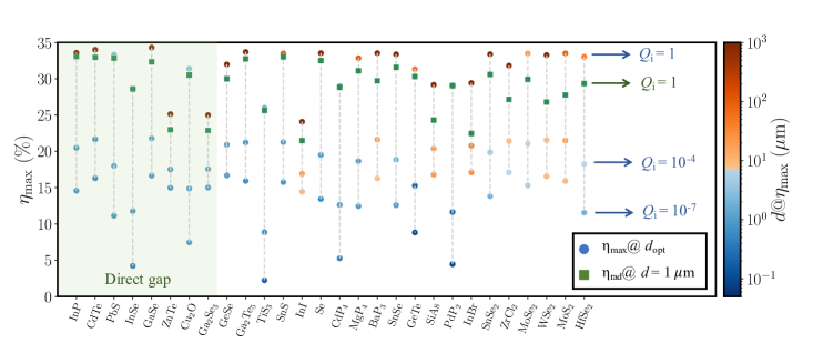
In Fig. 6, we show how varies with the amount of non-radiative recombination for some of the most promising materials. Here we vary from 1 (radiative limit) to 10-7 (dominant non-radiative recombination) and plot the corresponding maximum efficiency, , and optimal film thickness, , indicated by the color code. We also show at 1 m film thickness. In the SI we provide more detailed plots of versus film thickness for various values for (as in Fig. 3(c)) for all the materials in Fig. 6. The order of the materials in Fig. 6 is such that increases from left to right, i.e. direct band gap materials, indicated by green shaded region, are found to the left. Considering only when comparing a direct and indirect gap compound is not sufficient, as can be different for different materials. For example, CdTe has , whereas the known highest device efficiency is 22.1.Green et al. (2022) This efficiency is slightly higher than at =10-4. The measured on the highest-efficiency CdTe solar cell is Green and Ho-Baillie (2019), indicating that some additional loss mechanisms are present besides non-radiative recombination. At the same time, we can see a number of indirect gap materials which show , for practical (10-2-10-4) ranges. The optimal device thickness in case of indirect materials are higher mainly due to low absorption at the indirect gap. We can see a trend that with increasing the optimal device thickness (at different values) increases, which means with larger the suitability for thin film PV technology might reduce. Still, there are a number of indirect gap compounds showing excellent at thin film thickness range. These materials are discussed in the next section.
There has been a lot of discussion whether a small indirect gap can be beneficial for PV application.Hutter et al. (2017); Kirchartz and Rau (2017) With this study, we clarify how an indirect and direct gap material compare in the radiative limit for small film thicknesses (see SI section S7 for a detailed discussion). We find that at smaller film thicknesses (m), in the radiative limit (high mobility) adding a small indirect gap to a direct gap material will never show higher , as the gain in absorption (higher ) will be counteracted by higher radiative loss (lower ). However, an indirect gap material with small can exhibit higher compared to a direct gap material with same fundamental gap, as long as the gap is below the SQ maximum (1.1 eV). For example, an indirect gap material with = 0.95 eV and =0.1 eV can in principle show higher compared to a material with direct of 0.95 eV. This is mainly due to the opposite effect (higher gain in compared to loss in ) as discussed for the previous case. With this study, using our formalism we can provide real material examples here. For example, InSe is a direct gap material with =0.89 eV showing of 28.60%. In comparison, CdP4, which has an indirect gap of 0.86 eV and direct gap of 1.01 eV, shows higher of 28.83% (see Table I). More examples can be found in SI section S7 and related tables.
D. Discussion of final list of materials
Among the materials that pass all screening criteria, we discard the ones that have been shown to be unstable in air (elemental I, Cs2P3, Rb2P3, RbSb2, KSb2, Na3Sb, NaSe, YN). We also leave out the Tl-containing materials (Tl2O, Tl2Te3) due to serious toxicity concerns. Finally, we discard the Os- and Ru-containing materials (OsAs2, OsP2, RuP2) due to their very low earth abundance.
The final list of screened materials is presented in Table 1, grouped by maturity level. We note that all of the compounds have an ICSD-id, which means that they have been previously synthesized. CdTe, InP, and PbS are established materials which have been particularly successful in single-junction, multijunction, and quantum dot solar cells, respectively.
Among the emerging materials identified by our work, there are a few with record PCE above 5%. They are InSe Martínez‐Pastor et al. (1987), Cu2O Minami et al. (2016), elemental SeTodorov et al. (2017), and WSe2 Kim et al. (2022). The other emerging materials have been investigated for PV applications, but their record PCE is below 5% or they have not yet been incorporated in a working solar cell. Except for InI Dunlap-Shohl et al. (2018), all materials in this group are chalcogenides, and the large majority of them have 2D (layered) structures. Group IV, Ga-based, and transition-metal chalcogenides are particularly well represented. In many cases, the development of these layered compounds for PV applications has focused on extremely thin films, to take advantage of the enhanced light absorption that many of these compounds experience in atomically-thin form. ZnTe is a well known hole contact layer in CdTe PV technology, but it has also been tested as a wide-gap photoabsorber for tandem cell applications, although efficiencies are still very low Wang et al. (2011).
The ”rediscovery” of many already known PV materials lends credibility to our approach. We note that a few binary compounds with notable PV efficiencies, like Sb2S3 and Zn3P2, are missed by our approach because they have more than 12 atoms in their unit cell. We miss GaAs due to underestimation band gap using GLLB-SC functional (0.68 eV). We also miss CdSe because the calculated hole effective mass is higher than .
We find nine compounds that have not been previously studied as PV materials. We label them ”unexplored” in Table 1. To the best of our knowledge, none of these compounds have been synthesized as thin films, except for InBr Brothers et al. (1990). Intriguingly, none of these compounds belongs to traditional semiconductor families. What most of these semiconductors have in common is the existence of homoelement bonds, i.e., bonds between the same elements. This feature is absent in the currently known compound semiconductors for PV (III-V, II-VI, perovskites, and derivatives thereof). Due to this qualitative difference, the properties of these semiconductors with hybrid (homo- and heteroelement) bonding cannot be readily extrapolated from the properties of well-known semiconductors with only heteroelement bonds. Thus, these materials could be a new frontier of PV materials discovery.
Four compounds (CdP4, MgP4, BaP3, and PdP2) are phosphorus-rich phosphides, containing metal-P as well as P-P bonds. Due to these additional covalent bonds, phosphorus is in a higher oxidation state (ranging from -1 to -0.5) than the classic -3 state found in optoelectronic phosphides, e.g., InP, Zn3P2, and the II-IV-P2 ternaries. In general, phosphorus-rich phosphides have not been studied as potential PV materials before. They had hardly been grown in thin-film form until a very recent report of single-phase CuP2 films in the P21/c structure by reactive sputtering and soft annealing in an inert atmosphere Crovetto et al. .
In a similar spirit, TiS3 can be classified as a sulfur-rich sulfide due to the presence of both metal-S and S-S bonds. TiS3 has only been minimally investigated in photoelectrochemical cells and not in thin-film form Gorochov et al. (1983). In SiAs, all Si atoms are bonded to 3 As atoms and 1 Si atom, so Si can be considered as in the +3 oxidation state, thus explaining the 1:1 stoichiometry. There is one report of SiAs in a photoelectrochemical cell, but the sample was not in thin-film form Lewerenz and Wetzel (1983). In Ga2Te5, 20% of the Te atoms are only bonded to other 4 Te atoms (Te-Te bonds), and the remaining 80% is bonded to one Te atom and 2 Ga atoms.
On the other hand, the two halide compounds InBr and ZrCl2 do not have homoelement bonds and are quite different from each other. InBr should be qualitatively similar to the already known InI Dunlap-Shohl et al. (2018), but with a larger and a band gap closer to the SQ optimum. ZrCl2 is one of the first transition metal halides to be identified for potential PV applications. It has the same structure as 3R-MoS2 with Zr in the unusual +2 oxidation state. Unlike most of the known PV semiconductors, ZrCl2 has a lone valence band. It also has a large and reasonably low effective masses along its 2D layers.
Considering a combination of crustal abundance and elasticity of production Vesborg and Jaramillo (2012), we estimate that only five compounds from the ”unexplored” family could potentially be scaled to terawatt levels. These are TiS3, MgP4, BaP3, SiAs, and ZrCl2. These compounds deserve further investigation.
IV. Conclusion
In summary, we propose an efficient methodology to calculate phonon assisted absorption, which enables us to accurately evaluate optical absorption for indirect band gap materials. Using this method, along with various relevant photovoltaic (PV) descriptors (such as device efficiency, effective masses, internal luminescence quantum efficiency, etc.) we evaluate the potential of 127 experimentally known binary semiconductors (of which 97 are have indirect band gap) for thin film PV. After screening the materials based on the PV descriptors and considering toxicity, material abundance and air stability, we identify 28 promising materials of which 20 have an indirect gap. This list includes well established PV materials like InP, CdTe, PbS, as well as emerging ones such as, elemental Se, SnS, SnSe, SnSe2, lending credibility to our approach. Additionally, we discover 9 previously unexplored compounds with potential for thin film PV. Most of these compounds show homoelemental bonds and the constituent elements show deviation from their well known oxidation states. These materials (and their respective stoichiometric classes) have scarcely, if ever, been explored for photovoltaics and could become a new frontier of next generation PV materials research. Further theoretical work on these materials should address their defect tolerance, carrier mobilities and lifetimes. Such studies can benefit from our open database containing the calculated atomic and electronic structures as well as basic PV descriptors for the 127 materials investigated in this work.
V. Methodology
A. Computational Details
First principles calculations are performed using Density Functional Theory (DFT)Kohn and Sham (1965) within the Projector-Augmented Wave (PAW) formalismBlöchl (1994) as implemented in GPAW codeMortensen et al. (2005); Enkovaara et al. (2010), in combination with Atomic Simulation Environment (ASE)Larsen et al. (2017). A plane wave cutoff energy of 800 eV and k-mesh density of 8 Å-1 are employed for geometry optimization. Electronic structure calculations are performed using Perdew-Burke-Ernzerhof (PBE)Perdew et al. (1996) exchange correlation functional with double zeta polarized (dzp) basis setLarsen et al. (2009). The accuracy of dzp basis set was tested in a previous study and reported to produce phonon modes with fair accuracy Taghizadeh et al. (2020). The phonon modes are evaluated via calculating the dynamical matrices within the harmonic approximation. Force constant matrices are calculated using small displacement approachAlfè (2009) as implemented in ASE. Electron-phonon matrix elements are evaluated based on calculation of gradients of effective potential with finite difference technique Kaasbjerg et al. (2012) as implemented in GPAW. As our approximation involves only zone-center ( point) phonons, we use primitive unit cells for respective calculations. Next, the momentum matrix elements are obtained using the finite difference technique as implemented in GPAW. A real-space grid spacing of 0.2 Å is chosen for these calculations. We have used 161616 (8 Å-1) k-mesh (density) for systems with less (more) than 4 atoms in the unit cell, when evaluating the electron-phonon coupling matrix elements. For phonon calculations, 8 Å-1 (6 Å-1) k-mesh density is used for unit cells with less (more) than 4 atoms and the forces are converged until eV/Å. The width of the Fermi-Dirac smearing is kept at 50 meV. While calculating the probability of transition, the Dirac delta function is replaced with a Gaussian function with a smearing width of 40 meV, which accounts for inhomogeneous spectral broadening. The choice of PBE exchange-correlation functional which is known to slightly overestimate the lattice parameters and significantly underestimate the band gap values, is expected to have some effect on the calculated absorption coefficient and efficiency. In order to account for the band gap underestimation, we have calculated the band gaps with GLLB-SC functionalKuisma et al. (2010), which is known to produce accurate band gapsCastelli et al. (2015) and is highly affordable computationally. During the calculation of probability of transition, the conduction bands are scissor shifted to match the GLLB-SC gap. The effect of temperature is incorporated only into the phonon occupation numbers. We have considered = 298 K for all the calculations. Additional finite temperature effects (e.g. lattice expansion and electron-phonon renormalization, etc.) may exhibit effects on the absorption coefficient and as such device efficiency slightly. Optical absorption coefficient beyond the direct gap is obtained via calculating the frequency dependent dielectric function within the Random Phase Approximation (RPA) as implemented in GPAW. The computational workflow was constructed using the Atomic Simulation Recipes (ASR)Gjerding et al. (2021) and executed using the MyQueueMortensen et al. (2020) task scheduler frontend.
I Acknowledgements
We acknowledge funding from the European Research Council (ERC) under the European Union’s Horizon 2020 research and innovation program Grant No. 773122 (LIMA) and Grant agreement No. 951786 (NOMAD CoE). K. S. T. is a Villum Investigator supported by VILLUM FONDEN (grant no. 37789).
References
- Green et al. (2022) M. A. Green, E. D. Dunlop, J. Hohl‐Ebinger, M. Yoshita, N. Kopidakis, K. Bothe, D. Hinken, M. Rauer, and X. Hao, Solar cell efficiency tables (version 60), Progress in Photovoltaics: Research and Applications 30, 687 (2022).
- Yoshikawa et al. (2017) K. Yoshikawa, H. Kawasaki, W. Yoshida, T. Irie, K. Konishi, K. Nakano, T. Uto, D. Adachi, M. Kanematsu, H. Uzu, and K. Yamamoto, Silicon heterojunction solar cell with interdigitated back contacts for a photoconversion efficiency over 26%, Nature Energy 2, 17032 (2017).
- Wanlass (2017) M. Wanlass, Systems and methods for advanced ultra-high-performance InP solar cells, Tech. Rep. (National Renewable Energy Lab.(NREL), Golden, CO (United States), 2017).
- Green and Ho-Baillie (2019) M. A. Green and A. W. Ho-Baillie, Pushing to the limit: radiative efficiencies of recent mainstream and emerging solar cells, ACS Energy Letters 4, 1639 (2019).
- Nakamura et al. (2019) M. Nakamura, K. Yamaguchi, Y. Kimoto, Y. Yasaki, T. Kato, and H. Sugimoto, Cd-free cu (in, ga)(se, s) 2 thin-film solar cell with record efficiency of 23.35%, IEEE Journal of Photovoltaics 9, 1863 (2019).
- Min et al. (2021) H. Min, D. Y. Lee, J. Kim, G. Kim, K. S. Lee, J. Kim, M. J. Paik, Y. K. Kim, K. S. Kim, M. G. Kim, T. J. Shin, and S. Il Seok, Perovskite solar cells with atomically coherent interlayers on SnO2 electrodes, Nature 598, 444 (2021).
- Shockley and Queisser (1961) W. Shockley and H. J. Queisser, Detailed balance limit of efficiency of p-n junction solar cells, Journal of applied physics 32, 510 (1961).
- Tiedje et al. (1984) T. Tiedje, E. Yablonovitch, G. D. Cody, and B. G. Brooks, Limiting efficiency of silicon solar cells, IEEE Transactions on electron devices 31, 711 (1984).
- Yu and Zunger (2012) L. Yu and A. Zunger, Identification of potential photovoltaic absorbers based on first-principles spectroscopic screening of materials, Physical review letters 108, 068701 (2012).
- Blank et al. (2017) B. Blank, T. Kirchartz, S. Lany, and U. Rau, Selection metric for photovoltaic materials screening based on detailed-balance analysis, Physical review applied 8, 024032 (2017).
- Kim et al. (2020) S. Kim, J. A. Márquez, T. Unold, and A. Walsh, Upper limit to the photovoltaic efficiency of imperfect crystals from first principles, Energy & Environmental Science 13, 1481 (2020).
- Zhao et al. (2017) X.-G. Zhao, J.-H. Yang, Y. Fu, D. Yang, Q. Xu, L. Yu, S.-H. Wei, and L. Zhang, Design of lead-free inorganic halide perovskites for solar cells via cation-transmutation, Journal of the American Chemical Society 139, 2630 (2017).
- Kuhar et al. (2018) K. Kuhar, M. Pandey, K. S. Thygesen, and K. W. Jacobsen, High-throughput computational assessment of previously synthesized semiconductors for photovoltaic and photoelectrochemical devices, ACS Energy Letters 3, 436 (2018).
- Choudhary et al. (2019) K. Choudhary, M. Bercx, J. Jiang, R. Pachter, D. Lamoen, and F. Tavazza, Accelerated discovery of efficient solar cell materials using quantum and machine-learning methods, Chemistry of Materials 31, 5900 (2019).
- Li and Yang (2019) Y. Li and K. Yang, High-throughput computational design of organic–inorganic hybrid halide semiconductors beyond perovskites for optoelectronics, Energy & Environmental Science 12, 2233 (2019).
- Luo et al. (2021) S. Luo, T. Li, X. Wang, M. Faizan, and L. Zhang, High-throughput computational materials screening and discovery of optoelectronic semiconductors, Wiley Interdisciplinary Reviews: Computational Molecular Science 11, e1489 (2021).
- Dahliah et al. (2021) D. Dahliah, G. Brunin, J. George, V.-A. Ha, G.-M. Rignanese, and G. Hautier, High-throughput computational search for high carrier lifetime, defect-tolerant solar absorbers, Energy & Environmental Science 14, 5057 (2021).
- Gan et al. (2022) Y. Gan, N. Miao, P. Lan, J. Zhou, S. R. Elliott, and Z. Sun, Robust design of high-performance optoelectronic chalcogenide crystals from high-throughput computation, Journal of the American Chemical Society 144, 5878 (2022).
- Hutter et al. (2017) E. M. Hutter, M. C. Gélvez-Rueda, A. Osherov, V. Bulović, F. C. Grozema, S. D. Stranks, and T. J. Savenije, Direct–indirect character of the bandgap in methylammonium lead iodide perovskite, Nature materials 16, 115 (2017).
- Kirchartz and Rau (2017) T. Kirchartz and U. Rau, Decreasing radiative recombination coefficients via an indirect band gap in lead halide perovskites, The Journal of Physical Chemistry Letters 8, 1265 (2017).
- Noffsinger et al. (2012) J. Noffsinger, E. Kioupakis, C. G. Van de Walle, S. G. Louie, and M. L. Cohen, Phonon-assisted optical absorption in silicon from first principles, Physical review letters 108, 167402 (2012).
- Kang et al. (2018) Y. Kang, H. Peelaers, K. Krishnaswamy, and C. G. Van de Walle, First-principles study of direct and indirect optical absorption in basno3, Applied Physics Letters 112, 062106 (2018).
- Monserrat et al. (2018) B. Monserrat, C. E. Dreyer, and K. M. Rabe, Phonon-assisted optical absorption in basno 3 from first principles, Physical Review B 97, 104310 (2018).
- Menéndez et al. (2018) J. Menéndez, D. J. Lockwood, J. C. Zwinkels, and M. Noël, Phonon-assisted optical absorption in germanium, Physical Review B 98, 165207 (2018).
- Bravić and Monserrat (2019) I. Bravić and B. Monserrat, Finite temperature optoelectronic properties of bas from first principles, Physical Review Materials 3, 065402 (2019).
- Ha et al. (2020) V.-A. Ha, B. Karasulu, R. Maezono, G. Brunin, J. B. Varley, G.-M. Rignanese, B. Monserrat, and G. Hautier, Boron phosphide as a p-type transparent conductor: Optical absorption and transport through electron-phonon coupling, Physical Review Materials 4, 065401 (2020).
- Ge et al. (2020) Y. Ge, W. Wan, X. Guo, and Y. Liu, Direct and indirect optical absorptions of cubic bas and bsb, Optics Express 28, 238 (2020).
- Jian et al. (2021) C.-c. Jian, X. Ma, J. Zhang, and X. Yong, Strained mosi2n4 monolayers with excellent solar energy absorption and carrier transport properties, The Journal of Physical Chemistry C 125, 15185 (2021).
- Willis et al. (2022) J. Willis, I. Bravić, R. R. Schnepf, K. N. Heinselman, B. Monserrat, T. Unold, A. Zakutayev, D. O. Scanlon, and A. Crovetto, Prediction and realisation of high mobility and degenerate p-type conductivity in cacup thin films, Chemical Science 13, 5872 (2022).
- Perdew et al. (1996) J. P. Perdew, K. Burke, and M. Ernzerhof, Generalized gradient approximation made simple, Physical review letters 77, 3865 (1996).
- Grimme et al. (2010) S. Grimme, J. Antony, S. Ehrlich, and H. Krieg, A consistent and accurate ab initio parametrization of density functional dispersion correction (dft-d) for the 94 elements h-pu, The Journal of chemical physics 132, 154104 (2010).
- Svendsen et al. (2022) M. K. Svendsen, H. Sugimoto, A. Assadillayev, D. Shima, M. Fujii, K. S. Thygesen, and S. Raza, Computational discovery and experimental demonstration of boron phosphide ultraviolet nanoresonators, Advanced Optical Materials , 2200422 (2022).
- Kuisma et al. (2010) M. Kuisma, J. Ojanen, J. Enkovaara, and T. T. Rantala, Kohn-sham potential with discontinuity for band gap materials, Physical Review B 82, 115106 (2010).
- Shockley and Read Jr (1952) W. Shockley and W. Read Jr, Statistics of the recombinations of holes and electrons, Physical review 87, 835 (1952).
- Hall (1952) R. N. Hall, Electron-hole recombination in germanium, Physical review 87, 387 (1952).
- Huldt (1971) L. Huldt, Band-to-band auger recombination in indirect gap semiconductors, physica status solidi (a) 8, 173 (1971).
- Larsen et al. (2019) P. M. Larsen, M. Pandey, M. Strange, and K. W. Jacobsen, Definition of a scoring parameter to identify low-dimensional materials components, Physical Review Materials 3, 034003 (2019).
- Rasmussen and Thygesen (2015) F. A. Rasmussen and K. S. Thygesen, Computational 2d materials database: electronic structure of transition-metal dichalcogenides and oxides, The Journal of Physical Chemistry C 119, 13169 (2015).
- Kaasbjerg et al. (2012) K. Kaasbjerg, K. S. Thygesen, and K. W. Jacobsen, Phonon-limited mobility in n-type single-layer mos 2 from first principles, Physical Review B 85, 115317 (2012).
- Kaasbjerg (2020) K. Kaasbjerg, Atomistic t-matrix theory of disordered two-dimensional materials: Bound states, spectral properties, quasiparticle scattering, and transport, Physical Review B 101, 045433 (2020).
- Khoroshiltseva et al. (2016) M. Khoroshiltseva, D. Slanzi, and I. Poli, A pareto-based multi-objective optimization algorithm to design energy-efficient shading devices, Applied energy 184, 1400 (2016).
- Choi et al. (2020) M.-J. Choi, F. P. García de Arquer, A. H. Proppe, A. Seifitokaldani, J. Choi, J. Kim, S.-W. Baek, M. Liu, B. Sun, M. Biondi, et al., Cascade surface modification of colloidal quantum dot inks enables efficient bulk homojunction photovoltaics, Nature communications 11, 1 (2020).
- Martínez‐Pastor et al. (1987) J. Martínez‐Pastor, A. Segura, J. L. Valdés, and A. Chevy, Electrical and photovoltaic properties of indium‐tin‐oxide/ p ‐InSe/Au solar cells, Journal of Applied Physics 62, 1477 (1987).
- Minami et al. (2016) T. Minami, Y. Nishi, and T. Miyata, Efficiency enhancement using a Zn1-xGex-O thin film as an n-type window layer in Cu2O-based heterojunction solar cells, Applied Physics Express 9, 052301 (2016).
- Todorov et al. (2017) T. K. Todorov, S. Singh, D. M. Bishop, O. Gunawan, Y. S. Lee, T. S. Gershon, K. W. Brew, P. D. Antunez, and R. Haight, Ultrathin high band gap solar cells with improved efficiencies from the world’s oldest photovoltaic material, Nature communications 8, 1 (2017).
- Kim et al. (2022) K.-H. Kim, M. Andreev, S. Choi, J. Shim, H. Ahn, J. Lynch, T. Lee, J. Lee, K. N. Nazif, A. Kumar, et al., High-efficiency wse2 photovoltaic devices with electron-selective contacts, ACS nano (2022).
- Ishikawa et al. (2021) R. Ishikawa, P. J. Ko, R. Anzo, C. L. Woo, G. Oh, and N. Tsuboi, Photovoltaic characteristics of gase/mose2 heterojunction devices, Nanoscale Research Letters 16, 1 (2021).
- Wang et al. (2011) W. Wang, J. D. Phillips, S. J. Kim, and X. Pan, ZnO/ZnSe/ZnTe Heterojunctions for ZnTe-Based Solar Cells, Journal of Electronic Materials 40, 1674 (2011).
- Ho (2020) C.-H. Ho, Ga2se3 defect semiconductors: The study of direct band edge and optical properties, ACS omega 5, 18527 (2020).
- Liu et al. (2021) S.-C. Liu, Z. Li, J. Wu, X. Zhang, M. Feng, D.-J. Xue, and J.-S. Hu, Boosting the efficiency of gese solar cells by low-temperature treatment of pn junction, Science China Materials 64, 2118 (2021).
- Sinsermsuksakul et al. (2014) P. Sinsermsuksakul, L. Sun, S. W. Lee, H. H. Park, S. B. Kim, C. Yang, and R. G. Gordon, Overcoming efficiency limitations of sns-based solar cells, Advanced Energy Materials 4, 1400496 (2014).
- Dunlap-Shohl et al. (2018) W. A. Dunlap-Shohl, I. G. Hill, Y. Yan, and D. B. Mitzi, Photovoltaic Effect in Indium(I) Iodide Thin Films, Chemistry of Materials 30, 8226 (2018).
- Nandi et al. (2022) R. Nandi, P. S. Pawar, K. E. Neerugatti, J. Y. Cho, S. Kim, S. H. Cho, Y. S. Lee, and J. Heo, Vapor-transport-deposited orthorhombic-snse thin films: A potential cost-effective absorber material for solar-cell applications, Solar RRL 6, 2100676 (2022).
- Jones et al. (2016) A. M. Jones, R. A. Coutu, and R. A. Lake, Design and analysis of novel ge-gete pn junction for photovoltaics, in 2016 IEEE NAECON and OIS (IEEE, 2016) pp. 343–348.
- Yu et al. (2012) X. Yu, J. Zhu, Y. Zhang, J. Weng, L. Hu, and S. Dai, Snse 2 quantum dot sensitized solar cells prepared employing molecular metal chalcogenide as precursors, Chemical communications 48, 3324 (2012).
- Memaran et al. (2015) S. Memaran, N. R. Pradhan, Z. Lu, D. Rhodes, J. Ludwig, Q. Zhou, O. Ogunsolu, P. M. Ajayan, D. Smirnov, A. I. Fernandez-Dominguez, et al., Pronounced photovoltaic response from multilayered transition-metal dichalcogenides pn-junctions, Nano letters 15, 7532 (2015).
- Wi et al. (2014) S. Wi, H. Kim, M. Chen, H. Nam, L. J. Guo, E. Meyhofer, and X. Liang, Enhancement of photovoltaic response in multilayer mos2 induced by plasma doping, ACS nano 8, 5270 (2014).
- Afzal et al. (2021) A. M. Afzal, S. Mumtaz, M. Z. Iqbal, M. W. Iqbal, A. Manzoor, G. Dastgeer, M. J. Iqbal, Y. Javed, R. Khan, N. A. Shad, et al., Fast and high photoresponsivity gallium telluride/hafnium selenide van der waals heterostructure photodiode, Journal of Materials Chemistry C 9, 7110 (2021).
- Brothers et al. (1990) A. D. Brothers, F. J. Feuerborn, and S. E. Bauer, Excitons in Indium Halide Thin Films, physica status solidi (b) 158, 503 (1990).
- Crovetto et al. (0) A. Crovetto, D. Kojda, F. Yi, K. N. Heinselman, D. A. LaVan, K. Habicht, T. Unold, and A. Zakutayev, Crystallize it before it diffuses: Kinetic stabilization of thin-film phosphorus-rich semiconductor cup2, Journal of the American Chemical Society 0, null (0), pMID: 35822809, https://doi.org/10.1021/jacs.2c04868 .
- Gorochov et al. (1983) O. Gorochov, A. Katty, N. Le Nagard, C. Levy-Clement, and D. Schleich, Photoelectrochemical study of TiS3 in aqueous solution, Materials Research Bulletin 18, 111 (1983).
- Lewerenz and Wetzel (1983) H. Lewerenz and H. Wetzel, Photoeffect on sias electrodes, Journal of the Electrochemical Society 130, 1228 (1983).
- Vesborg and Jaramillo (2012) P. C. K. Vesborg and T. F. Jaramillo, Addressing the terawatt challenge: scalability in the supply of chemical elements for renewable energy, RSC Advances 2, 7933 (2012).
- Kohn and Sham (1965) W. Kohn and L. J. Sham, Self-consistent equations including exchange and correlation effects, Physical review 140, A1133 (1965).
- Blöchl (1994) P. E. Blöchl, Projector augmented-wave method, Physical review B 50, 17953 (1994).
- Mortensen et al. (2005) J. J. Mortensen, L. B. Hansen, and K. W. Jacobsen, Real-space grid implementation of the projector augmented wave method, Physical Review B 71, 035109 (2005).
- Enkovaara et al. (2010) J. Enkovaara, C. Rostgaard, J. J. Mortensen, J. Chen, M. Dułak, L. Ferrighi, J. Gavnholt, C. Glinsvad, V. Haikola, H. Hansen, et al., Electronic structure calculations with gpaw: a real-space implementation of the projector augmented-wave method, Journal of physics: Condensed matter 22, 253202 (2010).
- Larsen et al. (2017) A. H. Larsen, J. J. Mortensen, J. Blomqvist, I. E. Castelli, R. Christensen, M. Dułak, J. Friis, M. N. Groves, B. Hammer, C. Hargus, et al., The atomic simulation environment—a python library for working with atoms, Journal of Physics: Condensed Matter 29, 273002 (2017).
- Larsen et al. (2009) A. H. Larsen, M. Vanin, J. J. Mortensen, K. S. Thygesen, and K. W. Jacobsen, Localized atomic basis set in the projector augmented wave method, Physical Review B 80, 195112 (2009).
- Taghizadeh et al. (2020) A. Taghizadeh, U. Leffers, T. G. Pedersen, and K. S. Thygesen, A library of ab initio raman spectra for automated identification of 2d materials, Nature communications 11, 1 (2020).
- Alfè (2009) D. Alfè, Phon: A program to calculate phonons using the small displacement method, Computer Physics Communications 180, 2622 (2009).
- Castelli et al. (2015) I. E. Castelli, F. Hüser, M. Pandey, H. Li, K. S. Thygesen, B. Seger, A. Jain, K. A. Persson, G. Ceder, and K. W. Jacobsen, New light-harvesting materials using accurate and efficient bandgap calculations, Advanced Energy Materials 5, 1400915 (2015).
- Gjerding et al. (2021) M. Gjerding, T. Skovhus, A. Rasmussen, F. Bertoldo, A. H. Larsen, J. J. Mortensen, and K. S. Thygesen, Atomic simulation recipes: A python framework and library for automated workflows, Computational Materials Science 199, 110731 (2021).
- Mortensen et al. (2020) J. J. Mortensen, M. Gjerding, and K. S. Thygesen, Myqueue: Task and workflow scheduling system, Journal of Open Source Software 5, 1844 (2020).