Controlled quantum dot array segmentation via a highly tunable interdot tunnel coupling
Abstract
Recent demonstrations using electron spins stored in quantum dots array as qubits are promising for developing a scalable quantum computing platform. An ongoing effort is therefore aiming at the precise control of the quantum dots parameters in larger and larger arrays which represents a complex challenge. Partitioning of the system with the help of the inter-dot tunnel barriers can lead to a simplification for tuning and offers a protection against unwanted charge displacement. In a triple quantum dot system, we demonstrate a nanosecond control of the inter-dot tunnel rate permitting to reach the two extreme regimes, large GHz tunnel coupling and sub-Hz isolation between adjacent dots. We use this novel development to isolate a sub part of the array while performing charge displacement and readout in the rest of the system. The degree of control over the tunnel coupling achieved in a unit cell should motivate future protocol development for tuning, manipulation and readout including this capability.
Arrays of quantum dots (QDs) are identified as one possible road for scaling up electron spin-based quantum processors Vinet et al. (2018); Li et al. (2018); Veldhorst et al. (2017); Vandersypen et al. (2017). In this context, the ability to displace controllably individual electrons plays an important role for realizing elementary operations within the array. Displacement at the dot scale induces high fidelity coherent manipulation and interaction Petta et al. (2005); Brunner et al. (2011); Watson et al. (2018); Yoneda et al. (2018). Displacement at multi-dot scale enables array filling Mortemousque et al. (2021); Volk et al. (2019), and functionalities for long distance quantum interconnection Mortemousque et al. (2021); Mills et al. (2019a); Jadot et al. (2021). These displacement capabilities come with potential sources of errors such as incorrect positioning and tunneling while operating the electron spin qubits. It is therefore desirable to find protocols to minimize their impact on the rest of the qubits. The tunnel barrier control over a large range offers strategies to protect the electron spin information without losing quantum manipulation capabilities Eenink et al. (2019). In semiconductor devices, this method is commonly used to isolate QD arrays from electron reservoirs, thereby fixing the total number of charges in the system Bertrand et al. (2015); Yang et al. (2020).
Here we characterize the inter-dot tunnel rate from the sub-Hz to GHz regime and achieve complete isolation both from the reservoirs and the neighbor QD of up to three electrons. Then, we implement two functionalities demonstrating the potential of the array partitioning process. First, an improvement of metastable charge states lifetime and their readout at a fixed and optimized position, and then charge displacement and readout in the partitioned array.
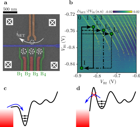
The device measured in this work is presented in Fig. 1a and is composed of a linear triple QD array defined electrostatically by voltages applied to metallic gates on a GaAs/AlGaAs heterostructure. The electrometer consists of a single electron transistor (SET) set on the side of a Coulomb peak to be sensitive to the charge configuration of the array. The QD array is tuned by adjusting the voltage applied on the gates labelled as . The gate voltages applied for each experiment discussed are summarized in Sup. Mat. I. We first focus on the protocol to isolate a quantum dot from the reservoirs. The first step is to load electrons from the bottom left reservoir (Fig. 1a) to the previously emptied QD nanostructure. We show in Fig. 1b, a so-called stability diagram where we vary the voltages applied on and while recording the current through the electrometer. In this diagram it is possible to determine the absolute number of electrons in the dot by identifying regions separated by charge degeneracy lines. The chemical potential of L is controlled by the voltage applied on while the reservoir to QD tunnel coupling is controlled by the voltage applied to , as indicated by the disappearance of the charge degeneracy lines for . The interruption of the degeneracy lines is an indicator of the isolated regime where the electron exchange rate with the reservoir is slower than the measurement sweep rate (250 mV/s). We engineered a pulse sequence to load the desired number of electrons in the QD structure and isolate them from the reservoir. The system is first initialized at point I empty of any electrons and the pulse sequence drawn on top of the stability diagram of Fig. 1b is applied. A voltage pulse on gate increases the coupling between the array and the reservoir, allowing the exchange of electrons with dot L. Then the chemical potential of the left QD is lowered by applying a voltage pulse on gate . By varying the amplitude of this pulse to reach either the point , or it is possible to load respectively 1, 2 or 3 electrons in the dot. A sketch of the potential landscape at the position is pictured in Fig. 1c. From the selected position, voltage pulses are applied on gate and then to reach the position I, where the electron tunneling to the reservoir is suppressed (see Sup. Mat. II). In this configuration, the high chemical potential of the left QD guarantees that all loaded electrons should eventually tunnel back to the reservoir leaving the QD empty. However, due to the low tunnel coupling to the reservoir this metastable configuration can be held for several tens of seconds (see Sup. Mat. II).
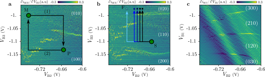
In this section, the isolation process is pushed one step further to perform array partitioning by demonstrating QD-to-QD decoupling. We note the charge configuration of the array with , and the charge occupation of the QDs L, M and R, respectively. After loading either 1, 2 or 3 electrons in L, we vary the voltages applied on and to progressively transfer charges to dot M. The corresponding stability diagrams are presented in Fig. 2a, b, c. For a system of dots containing a total of electrons, we expect charge states, which we experimentally observe for and up to 3. Analogous to the QD-reservoir decoupling, we observe the apparition of stochastic events as becomes increasingly more negative. This phenomenon now corresponds to the L-M inter-dot tunnel rate becoming comparable to the measurement sweep rate (250 mV/s).
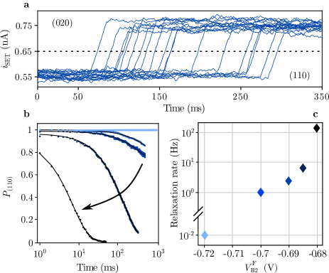
In order to quantify the inter-dot tunnel rate dependence with the voltage applied on gate , we designed the pulse sequence sketched on top of the stability diagrams in Fig. 2b. Two electrons are loaded in L and the system is brought in the configuration at position S. From this point, the tunnel coupling is lowered to the desired value using a voltage pulse on the gate . After 100 ns the detuning is set to reach the charge region via a voltage pulse on gate . At this position the charge state becomes metastable. To track the evolution of the charge state, we record the current during up to 1 s. The procedure is repeated 1000 times for between -0.72 V and -0.68 V. Selected records of for are shown in Fig. 3a and we observe sharp single jumps of from 0.55 nA to 0.75 nA. These events are associated to an electron tunneling from M to L. In Fig. 3b we compute the probability to observe the charge state as a function of the waiting time at point F and observe an exponential decay of the population. In Fig. 3c, we observe that the charge state lifetime can be tuned over 4 orders of magnitude in few tens of mV. In particular, for , no relaxation events are visible in a thousand 1 s-long time-traces, setting a higher tunnel rate bound at Hz. This demonstrates that we are able to reduce the inter-dot tunnel rate well below the Hz regime while keeping the initial QD structure intact. Moreover, the high level of control in the low inter-dot tunnel coupling regime did not prevent us to perform spin qubit operation which requires a GHz tunnel coupling in the same sample with the same tuning (data not shown here).
The capability to operate over such a wide range the inter-dot tunnel coupling enables novel functionalities for future prospects in spin qubit technology Li et al. (2018). Indeed, freezing on a fast timescale the electron dynamics results in a well separated and metastable charge configuration that can be efficiently probed. Proof of principle experiment is performed in a tunnel coupled double quantum dot (DQD) with up to three electrons. The protocol consists in loading a specific charge configuration in the double dot, decrease on fast timescale the tunnel barrier and then tune the system to a working point at which the charge detection has been optimized while preserving the charge configuration.
To do so we manipulate the inter-dot tunnel coupling and the detuning of the L-M DQD at the nanosecond timescale. The initialization of metastable charge configuration of the array is characterized using a freeze map protocol. It consists in setting the system at a given detuning and tunnel coupling value before pulsing the inter-dot tunnel rate to the sub-Hz regime to freeze the charge configuration. Followed by a charge readout, this protocol allows us to identify the detuning and tunnel coupling regions where a charge transfer is possible.
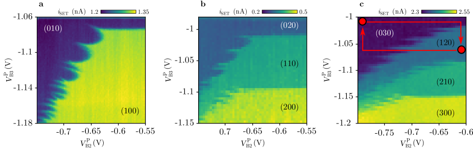
In addition to the already described notation for labelling the charge states we introduce a vertical bar indicating a sub-Hz tunnel coupling rate in between the QDs. The trajectory, visible in Fig. 2a, starts in the charge state at point M and is used to realize the freeze map protocol. Two 100 ns voltages pulses applied sequentially to and set the system to point P. Then, the inter-dot tunnel rate is lowered to the sub- regime and the detuning is set back to position M. At this position the electrometer signal is averaged during 5 ms. Depending on the coordinates of point P(,), we obtain two possible values for corresponding to either the or charge state, as shown in Fig. 4a. Comparing with the stability diagram in Fig. 2a, for we observe the same charge transition at . It indicates that the time spent at P is sufficient to observe charge transfer. For , the tunnel coupling rate is not strong enough to allow charge transfer in the ground state at . Nevertheless, by increasing the detuning () higher orbital states of M with higher tunnel coupling are accessible and allow the charge transfer within the time spent in P. The complete description of the charge dynamics to account for the precise shape of the charge transition is beyond the scope of this work and will be studied further in subsequent experiments. The agreement between the freeze map and the stability diagram is also observed for 2 and 3 electrons loaded in the array as shown in Fig. 4b,c. To conclude, we demonstrated the capability to initialize metastable charge configuration for a duration long enough to permit their readout at an optimized position in the voltage gate space. This study is a first demonstration of the novel initialization and readout protocols induced by the high level of control over the inter-dot tunnel coupling.
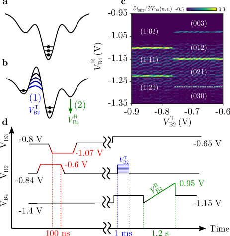
In addition to an improvement of the charge determination in QD arrays, the inter-dot tunnel coupling control also grants us the possibility to isolate subparts of a QD array to simplify the tuning and manipulation. In this section we demonstrate the complete isolation of a sub part of the QD array while keeping the complete control over the charge configuration in the rest of the system. To do so we initialize a metastable charge state of the L-M DQD in order to isolate an electron in L. Then we progressively transfer the charges remaining in M to R to control the number of electrons present in the M-R DQD subsystem.
The first step to implement this protocol consists in loading 3 electrons in M to reach the (030) charge state. From there, a () metastable charge configuration is initialized by pulsing the voltages applied on gate and , an equivalent of the pulse sequence performed is sketched on top of the freeze map in Fig. 4c. The next step consists in opening the tunneling between M and R by applying -0.65 V on gate , and lowering the chemical potential of R closer to the one of M by increasing the voltage applied on to -1.15 V. In this voltage configuration the L-M inter-dot tunnel coupling is pulsed during 1 ms using a voltage pulse of amplitude . Following the pulse, the detuning of L-R is ramped using the voltage applied on gate while is recorded. The derivative is plotted as a function of and in Fig. 5c. For we observe two degeneracy lines in the stability diagram indicating that the sub array composed of M and R QDs contains only two electrons while the third one is isolated in L. Due to the low L-M inter-dot tunnel coupling, the electron in L cannot tunnel back to M during the whole 1.2 s ramp, in this configuration the only charge states available by the array are , and (see Sup. Mat. III). They are identified and labelled on top of the stability diagram. For a pulse amplitude , we observe a third line, indicating that the electron stored in L tunneled back to M during the pulse. Indeed, this configuration allows the relaxation of the (120) to the (030) charge state and the resulting stability diagram corresponds to a classical one for three electrons loaded in a DQD. To conclude, we are able to perform electron manipulation in a partitioned DQD while preserving the charge state in the adjacent QD. This study demonstrates the ability of the array partitioning to lower the complexity of the stability diagrams by reducing the number of charge states available for the electrons.
The control of the tunnel couplings and the chemical potential of each QD on fast timescales allowed us to initialize arbitrary metastable charge state of up to three electrons in a DQD. The freeze map protocol developed in this article allowed us to enhance the lifetime and perform readout of these states at a fixed and optimized position in the voltage gate space. This demonstration is of particular interest in the context of the wide use of Pauli spin blocked spin to charge conversion whose fidelity is limited by the lifetime of such metastable charge states Barthel et al. (2009). We finally performed a segmentation of the array by decoupling a QD filled with one electron while performing charge displacement and readout in the rest of the structure. Doing so we observed a reduction of the charge states available for the system and therefore a reduction of the complexity while tuning the QD array. The partitioning protocol opens the door to more complex applications such as the operation of larger 1D or 2D arrays of QDs while keeping the low dimensionality of simple sub systems Mills et al. (2019b).
See supplementary material for additional information of the array tuning and the array partitioning protocol.
We acknowledge technical support from the Pole groups of the Institut Néel, and in particular the NANOFAB team who helped with the sample realization, as well as T. Crozes, E. Eyraud, D. Lepoittevin, C. Hoarau and C. Guttin. This work is supported by the ERC QUCUBE. A.L. and A.D.W. acknowledge gratefully support of DFG-TRR160 and DFH/UFA CDFA-05-06, DFG project 383065199, and BMBF QR.X Project 16KISQ009.
The data that support the findings of this study are available from the corresponding author upon reasonable request.
The authors have no conflicts to disclose.
M.N. and V.T. fabricated the sample. M.N. performed the experiment with the help of B.J. M.N. interpreted the data with the help of B.J., P.-A.M., E.C., M.D. and T.M. A.L. and A.D.W. performed the design and molecular-beam-epitaxy growth of the high-mobility heterostructure. All the authors discussed the results extensively, as well as the manuscript.
References
- Vinet et al. (2018) M. Vinet, L. Hutin, B. Bertrand, S. Barraud, J.-M. Hartmann, Y.-J. Kim, V. Mazzocchi, A. Amisse, H. Bohuslavskyi, L. Bourdet, A. Crippa, X. Jehl, R. Maurand, Y.-M. Niquet, M. Sanquer, B. Venitucci, B. Jadot, E. Chanrion, P.-A. Mortemousque, C. Spence, M. Urdampilleta, S. De Franceschi, and T. Meunier, “Towards scalable silicon quantum computing,” in 2018 IEEE International Electron Devices Meeting (IEDM) (2018) pp. 6.5.1–6.5.4.
- Li et al. (2018) R. Li, L. Petit, D. P. Franke, J. P. Dehollain, J. Helsen, M. Steudtner, N. K. Thomas, Z. R. Yoscovits, K. J. Singh, S. Wehner, L. M. K. Vandersypen, J. S. Clarke, and M. Veldhorst, “A crossbar network for silicon quantum dot qubits,” Science Advances 4, eaar3960 (2018).
- Veldhorst et al. (2017) M. Veldhorst, H. G. J. Eenink, C. H. Yang, and A. S. Dzurak, “Silicon CMOS architecture for a spin-based quantum computer,” Nature Communications 8, 1766 (2017).
- Vandersypen et al. (2017) L. M. K. Vandersypen, H. Bluhm, J. S. Clarke, A. S. Dzurak, R. Ishihara, A. Morello, D. J. Reilly, L. R. Schreiber, and M. Veldhorst, “Interfacing spin qubits in quantum dots and donors—hot, dense, and coherent,” npj Quantum Information 3, 34 (2017).
- Petta et al. (2005) J. R. Petta, A. C. Johnson, J. M. Taylor, E. A. Laird, A. Yacoby, M. D. Lukin, C. M. Marcus, M. P. Hanson, and A. C. Gossard, “Coherent Manipulation of Coupled Electron Spins in Semiconductor Quantum Dots,” Science 309, 2180–2184 (2005).
- Brunner et al. (2011) R. Brunner, Y.-S. Shin, T. Obata, M. Pioro-Ladrière, T. Kubo, K. Yoshida, T. Taniyama, Y. Tokura, and S. Tarucha, “Two-Qubit Gate of Combined Single-Spin Rotation and Interdot Spin Exchange in a Double Quantum Dot,” Physical Review Letters 107, 146801 (2011).
- Watson et al. (2018) T. F. Watson, S. G. J. Philips, E. Kawakami, D. R. Ward, P. Scarlino, M. Veldhorst, D. E. Savage, M. G. Lagally, M. Friesen, S. N. Coppersmith, M. A. Eriksson, and L. M. K. Vandersypen, “A programmable two-qubit quantum processor in silicon,” Nature 555, 633–637 (2018).
- Yoneda et al. (2018) J. Yoneda, K. Takeda, T. Otsuka, T. Nakajima, M. R. Delbecq, G. Allison, T. Honda, T. Kodera, S. Oda, Y. Hoshi, N. Usami, K. M. Itoh, and S. Tarucha, “A quantum-dot spin qubit with coherence limited by charge noise and fidelity higher than 99.9%,” Nature Nanotechnology 13, 102–106 (2018).
- Mortemousque et al. (2021) P.-A. Mortemousque, E. Chanrion, B. Jadot, H. Flentje, A. Ludwig, A. D. Wieck, M. Urdampilleta, C. Bäuerle, and T. Meunier, “Coherent control of individual electron spins in a two-dimensional quantum dot array,” Nature Nanotechnology 16, 296–301 (2021).
- Volk et al. (2019) C. Volk, A. M. J. Zwerver, U. Mukhopadhyay, P. T. Eendebak, C. J. van Diepen, J. P. Dehollain, T. Hensgens, T. Fujita, C. Reichl, W. Wegscheider, and L. M. K. Vandersypen, “Loading a quantum-dot based “Qubyte” register,” npj Quantum Information 5, 1–8 (2019).
- Mills et al. (2019a) A. R. Mills, D. M. Zajac, M. J. Gullans, F. J. Schupp, T. M. Hazard, and J. R. Petta, “Shuttling a single charge across a one-dimensional array of silicon quantum dots,” Nature Communications 10, 1063 (2019a).
- Jadot et al. (2021) B. Jadot, P.-A. Mortemousque, E. Chanrion, V. Thiney, A. Ludwig, A. D. Wieck, M. Urdampilleta, C. Bäuerle, and T. Meunier, “Distant spin entanglement via fast and coherent electron shuttling,” Nature Nanotechnology 16, 570–575 (2021).
- Eenink et al. (2019) H. G. J. Eenink, L. Petit, W. I. L. Lawrie, J. S. Clarke, L. M. K. Vandersypen, and M. Veldhorst, “Tunable Coupling and Isolation of Single Electrons in Silicon Metal-Oxide-Semiconductor Quantum Dots,” Nano Letters 19, 8653–8657 (2019).
- Bertrand et al. (2015) B. Bertrand, H. Flentje, S. Takada, M. Yamamoto, S. Tarucha, A. Ludwig, A. D. Wieck, C. Bäuerle, and T. Meunier, “Quantum Manipulation of Two-Electron Spin States in Isolated Double Quantum Dots,” Physical Review Letters 115, 096801 (2015).
- Yang et al. (2020) C. H. Yang, R. C. C. Leon, J. C. C. Hwang, A. Saraiva, T. Tanttu, W. Huang, J. Camirand Lemyre, K. W. Chan, K. Y. Tan, F. E. Hudson, K. M. Itoh, A. Morello, M. Pioro-Ladrière, A. Laucht, and A. S. Dzurak, “Operation of a silicon quantum processor unit cell above one kelvin,” Nature 580, 350–354 (2020).
- Barthel et al. (2009) C. Barthel, D. J. Reilly, C. M. Marcus, M. P. Hanson, and A. C. Gossard, “Rapid Single-Shot Measurement of a Singlet-Triplet Qubit,” Physical Review Letters 103, 160503 (2009), arXiv:0902.0227 .
- Mills et al. (2019b) A. R. Mills, M. M. Feldman, C. Monical, P. J. Lewis, K. W. Larson, A. M. Mounce, and J. R. Petta, “Computer-automated tuning procedures for semiconductor quantum dot arrays,” Applied Physics Letters 115, 113501 (2019b).