Designing, Building, and Characterizing RF Switch-based Reconfigurable Intelligent Surfaces
Abstract.
In this paper, we present our experience designing, prototyping, and empirically characterizing RF Switch-based Reconfigurable Intelligent Surfaces (RIS). Our RIS design comprises arrays of patch antennas, delay lines and programmable radio-frequency (RF) switches that enable passive 3D beamforming, i.e., without active RF components. We implement this design using PCB technology and low-cost electronic components, and thoroughly validate our prototype in a controlled environment with high spatial resolution codebooks. Finally, we make available a large dataset with a complete characterization of our RIS and present the costs associated with reproducing our design.
1. Introduction
Reconfigurable Intelligent Surfaces (RISs) are well-perceived as a key technology for next-generation mobile systems (Pan et al., 2021). Despite the recent hype on the topic, mostly driven by theoretical models and simulations, empirical studies are scarce due to lack of accessible and affordable RIS prototypes.
A RIS is essentially a planar structure with passive reflective cells that can control the electromagnetic response of impinging radio-frequency (RF) signals, such as changes in phase, amplitude, or polarization. Indeed, RISs open a new paradigm (Albanese et al., 2022) where the wireless channel—traditionally treated simply as an optimization constraint—plays an active role subject to optimization with the potential of increasing the energy efficiency of mobile networks by (Yang et al., 2022).
To this end, a RIS must satisfy the following requirements: () RISs shall (re-)steer RF signals with minimal power loss; () RISs must not use active RF components; () RISs must minimize the energy required to re-configure their reflective cells; () RISs shall be re-configurable in real-time; and () RISs must be amenable to low-cost production at scale.
Related Work. Among existing literature on prior experiences, (Yezhen et al., 2020) discloses a x RIS operating at GHz, whereas (Trichopoulos et al., 2021) introduces a x RIS working at sub-GHz with an Arduino control unit where only groups of elements can be configured. Both solutions implement a PIN diode-based RIS with a -bit resolution phase shift. Additionally, the prototype presented in (Dai et al., 2020) obtains a -bit phase quantization by using PIN diodes per RIS element, whereas in (Hu et al., 2020) the use of PIN diodes allows for phase states. (Fara et al., 2021) discloses a x RIS based on varactor diodes, which allows continuous control of the phase shifts at the cost of a wide range in control voltages, which is generally hard to achieve.
Conversely, RF switch-based implementations unveil a lower cost w.r.t. PIN diodes used to control the reflector units. In particular in (Tan et al., 2018), a RIS prototype with x reflectors at GHz is presented. The unit elements are placed more than one away to reduce the mutual coupling at the expense of a tighter maximum scanning angle ( is the operating wavelength). In (Arun and Balakrishnan, 2020), reflectors are mounted on the boards, they are tall, wide, and separated on both the x and y-axis. Finally, (Dunna et al., 2020) allows singular configurations of the elements, thereby reducing the number of utilized pins at controller side. This RIS is made of x patch antennas operating at GHz and controlled with -bit phase shifter made with the transmission line method.
Our design. Besides meeting the usual requirements for a RIS, our approach provides additional features compared to previous work. First, in contrast to diode-based approaches, usually constrained to 1-bit phase shifters, our design has a resolution of 3 bits, enabling high spatial resolution codebooks.
Second, our design permits coordinating multiple () boards, and hence it enables larger-scale structures of surfaces in a modular and flexible manner.
Finally, in addition to producing phase shifts onto impinging signals in a programmable manner, we can configure individual cells to fully absorb the energy of RF signals, which open several opportunities. For instance, we can effectively switch off reflective components, which let us virtually optimize the shape and the size of the RIS to meet system constraints. We would like to remark that switching off a cell in a RIS is not trivial when a cell is specifically designed to reflect signals passively, without a direct energy feed that could be cut off.
2. RIS design
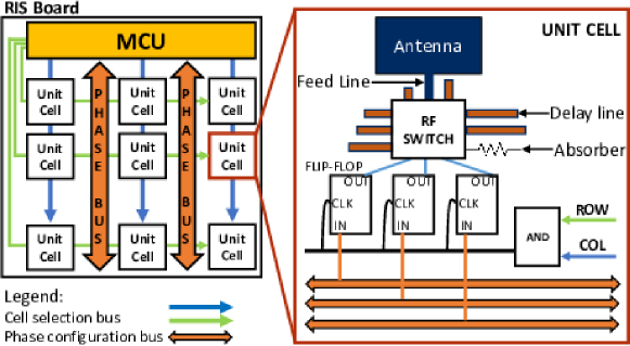
The main purpose of our RIS is to perform 3D beamforming passively, i.e., re-focus the energy received from impinging RF signals towards specified directions without active (energy-consuming) RF components. Fig. 1 illustrates a board consisting of a grid of unit cells distributed in a 2D array. Unit cells are elements that can reflect RF signals with configurable phase shifts.
Phase shifts are configured by a microcontroller unit (MCU), which can be programmed from an external controller. Conventional RIS designs are characterized by dedicated connections from the MCU to each unit cell. However, MCUs only support a limited number of such connections, which constrains the maximum number of cells and, consequently, the achievable beamforming gains (Mursia et al., 2021). A more scalable approach is to connect each cell with a pair of buses, denoted as column/row cell selection buses, that select the cell to be configured, and a phase configuration bus, which communicates the desired configuration index out of a discrete set. In this way, we reduce the complexity of the design from to connections per board.
As shown in the right-hand side of Fig. 1, each unit cell connects both column/row selection buses with an AND gate. Hence, when the MCU sets a high voltage state in row and column , the MCU activates the configuration bus for unit cell , whereas all the remaining gates across the board will output a low voltage state ( V). Each cell also integrates a set of flip-flop D, which exploit the high-state exiting the AND gate as a rising edge to update and send out the value stored in memory. We designed our RIS with 3-bit phase shifters, which enable high spatial resolution codebooks. Therefore, each cell uses three 1-bit phase configuration buses and three flip-flops.
The latter are connected to configuration ports in an RF switch. An RF switch is a component that can redirect the RF signal received from an input port towards one output port, as indicated by the configuration ports. The input port is connected to a patch antenna, the ultimate responsible for interacting with the medium, through a feeding line. Each output port (except one) uses an open-ended delay line with a suitably-designed length to reflect impinging signals with a specific time delay, shifting the signal phase.
We reserve one output port of the RF switch to connect an absorber, an impedance-matching component that absorbs the energy of incoming signals instead of reflecting them back. We call this configuration absorption state, and it let us virtually optimize the reflective area of the RIS to meet system constraints. For instance, we can flexibly adapt to different time constraints when optimizing the RIS configuration (which takes longer the larger the number of active cells in the RIS. This is illustrated in Fig. 3. Alternatively, an energy harvester (Mir et al., 2021) may be employed instead to re-use the dissipated energy to feed a low-consuming MCU, becoming self-sustainable boards, which we leave for future work.
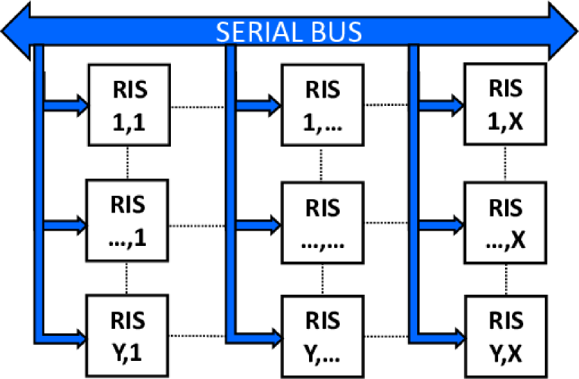
Our RIS design is modular: as shown in Fig. 3, multiple boards can be coordinated through a common bus. The disposition of the unit cells across different boards has been carefully designed to have a separation of , where is the operating wavelength. Such modular boards let us increase/decrease the physical area of our structure without compromising the inter-cell distance, as depicted in Fig. 3.
3. Beamforming codebook
A RIS board can be modelled as a uniform planar array (UPA) comprised of antenna elements (Basar et al., 2019; Mursia et al., 2021). Hence, we define the array response at the RIS for the steering angles , along the azimuth and elevation, respectively, as
| (1) | ||||
where is the ratio between the antenna spacing and the signal wavelength (usually ). Assuming line-of-sight signal propagation and a single-antenna transmitter, the channel between the latter and the RIS is given by
| (2) |
where we define the average channel power gain as , with the average channel power gain at a reference distance. represents the distance between the transmitter and the RIS, whereas , denote the angles of arrival at the RIS along the azimuth and elevation, respectively. With similar reasoning, the channel between the RIS and the single-antenna receiver is given by
| (3) |
The matrix containing the RIS configuration is defined as
| (4) |
with and the quantized RIS phase shift set. Note that, to preserve a tractable model in (4), we have neglected any phase-dependent reflection coefficient at the RIS. Lastly, the received signal at the receiver is given by
| (5) |
where is the transmitted symbol and is the noise term distributed as .
Let and , such that the power at the receiver is maximized by letting (Wu et al., 2018)
| (6) |
where projects each element of the vector in (6) onto the closest element of set to obtain a feasible solution.
It is important to highlight that vector has the form of a scaling term times the UPA response vector in (1) for some steering angles . Hence, in order to design a codebook of RIS beamforming vectors, we artificially create pairs of couples and generate the corresponding UPA response vectors . Given the symmetry of the array response around the -axis for the azimuth and around the -axis for the elevation, and in the interest of saving measurement time, we sample a regular grid of points spaced by degrees in the search space , such that . Finally, we obtain the RIS configurations for each steering angle couple in the codebook by applying the expression in (6).
4. Prototype Implementation
We prototyped our design using a two-layer PCB (Printed Circuit Board). The substrate material is FR-4, a composite material made of woven fiberglass with an epoxy resin binder that is flame resistant. Its relative electrical permittivity is in the range of , and is coated by two layers of 1-ounce copper (35). In general, thick substrates and high permittivity lead to small bandwidths and low efficiency due to surface waves (Pandey, 2019). Since the operating frequency of our prototype is GHz ( mm), we chose a substrate thickness of mm, that is in the range as suggested in (Pandey, 2019).
4.1. Patch Antenna
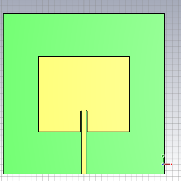
Patch antennas are implemented by cutting out a particular shape from the copper of the board’s upper layer. In this way, the remaining metallic shape can radiate at the desired frequency while the back layer operates as ground for the antenna. Following the conventional literature on antenna design, we used a rectangular shape, as shown in Fig. 5. In more detail, we used the transmission-line model from (Balanis, 2016) to calculate its width and length as follows:
| (7) | ||||
| (8) |
where is the effective dielectric constant that takes into account the fact that the electric field lines reside in the substrate and partially in the air, is the effective length, is the speed of light, and is an offset to obtain the antenna physical length from (see (Balanis, 2016) for details).
As shown in Fig. 5, a microstrip connects each antenna to the RF switch. To this end, we selected an inset feeding approach, with a notch at the edge of the antenna. This approach allows us to adapt the antenna to a precise characteristic impedance, which is crucial to maximizing power transfer. Given this notch (see details later), we refined the geometry derived before with the parameters shown in Fig. 5 by exhaustive search using a full-wave simulator (Dassault Systèmes, 2022), thus setting and .
In the following we describe in detail two crucial parameters, namely () the width of the microstrip that connects the RF switch (see Fig. 1), and () the position of the notch. The former is essential to guarantee impedance-matching, and, since the usual characteristic impedance is 50 , the width of all the microstrips must be selected accordingly.
4.1.1. Width of the feeding line
To avoid power loss between the feeding line and the RF switch, their characteristic impedance should match. Therefore, we used the model described in (Analog Devices, 2009) to estimate a -mm line width, which equalizes the -impedance of the switch.
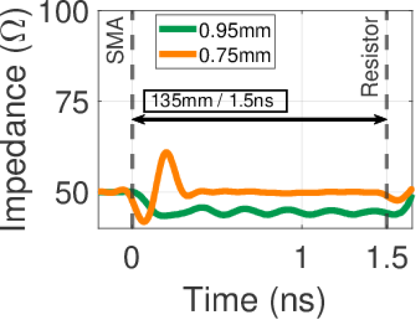
To validate this, we printed a mm-width microstrip and applied the Time Domain Reflectometry (TDR) technique using a Vector Network Analyzer (VNA) to measure the actual characteristic impedance along the line. TDR generates a pulse with a short rising time that allows us to calculate the impedance along the line based on the received reflections.
As depicted in Fig. 5 (green), this experiment shows that the actual impedance along the line is smaller than the predicted . Such a mismatch with the impedance of the switch would incur some power loss at every unit cell and, consequently, poor beamforming gains overall.
Consequently, we opted for a simple empirical approach: we printed out several mm-length microstrips with different widths, and applied the TDR method to each sample. Fig. 5 shows with an orange line the result of the selected sample, with a width equal to 0.75 mm, which provided the best performance. Ignoring the large oscillation at the beginning of the line, which is due to the soldered SMA connector that we used to connect the line and the VNA, the experiment shows a perfect match with the expected value of .
4.1.2. Notch
The second relevant parameter is the depth of the notch, which should minimize the amount of reflected power. This is achieved when the impedance of the antenna matches that of the feeding line. However, the antenna’s impedance diminishes as one moves towards its center because the current’s intensity is higher at that point. Hence, it is important to carefully design the depth of the notch.
Following the analytical method introduced in (Balanis, 2016), we first estimated the impedance at the bottom edge of the antenna and centered on the horizontal plane (see red bullet in Fig. 5). At this point, the impedance is purely resistive, i.e., its reactance is zero, and should be equal to (we omit the details of the mathematical model, which can be found in (Balanis, 2016), to reduce clutter). Then, the optimal depth of the notch can be computed as:
| (9) |
where is the desired impedance (i.e., ).
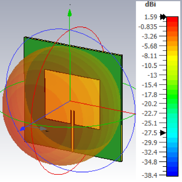
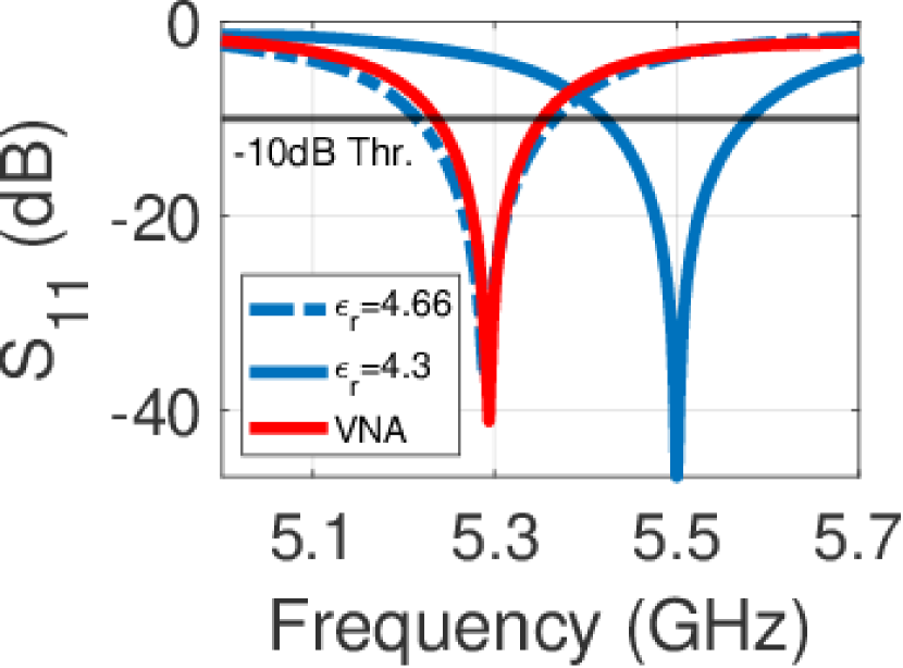
We attempted to validate this result with the full-wave simulator (Dassault Systèmes, 2022) and found that a -mm depth, cutting across the patch antenna as shown in Fig. 5, maximizes performance ( difference with respect to the model). Fig. 7 shows with a blue line the amount of power that is reflected, estimated by the simulator and referred to as S11 parameter in antenna design. The result shows good performance at 5.5 GHz, the operating frequency of choice. Fig. 7 shows the simulated radiation pattern, with minimal backwards propagation. Note that the antenna is not very directive and has an expected gain of 1.5dBi, which is common for this type of low-cost antennas.
To validate the patch design, we printed a sample antenna with the aforementioned parameters. Using our VNA, we measured the empirical and plotted the result with a red line in Fig. 7. Perhaps surprisingly, the minimal- frequency point is 5.3 GHz instead of the intended 5.5 GHz. After some research, we realized that the offset stems from an error on the nominal permittivity used in our model/simulations for the PCB substrate. After some iterations with our simulator, we estimated the real permittivity to be . In light of this, we changed the operating frequency to GHz.
From Fig. 7, we can also estimate that the bandwidth of our approach, i.e., the range of frequencies where the antenna’s is dB, is 118MHz (note the black horizontal line). We finally note that, at 5.3 GHz, the is dB, which corresponds to a Voltage Standing Wave Ration (VSWR) of . This means that the amount of power from the feeding line that is reflected back is negligible, which was our goal.
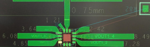
| Output port | 7 | 6 | 5 | 1 | 3 | 2 | 4 |
|---|---|---|---|---|---|---|---|
| (deg) | 51.42 | 102.85 | 154.28 | 205.71 | 257.14 | 308.57 | 360 |
| (mm) | 1.21 | 2.42 | 3.64 | 4.85 | 6.08 | 7.28 | 8.49 |
4.2. Phase shifters
At each cell, a specific phase shift is applied by routing the RF signal towards a specific delay line, implemented with a microstrip, that reflects the signal back to the patch antenna. To this end, we use a 3-bit RF switch SKY13418-485LF (Skyworks Solutions, Inc, 2019), which has 1 input port (attached to the feeding line), 3 configuration ports (more later), and 8 output ports connected to delay lines of different lengths. Given one configuration (input-output port mapping encoded as 3 bits in the configuration ports), the resulting phase shift follows as:
| (10) |
where denotes the distance travelled from the patch antenna to the end of the delay line (including the switch and the feeding and delay lines), and is the velocity factor of the microstrip material. Note that accounts for the round-trip between antenna and delay line.
To estimate empirically, we take advantage of the TDR technique used earlier, which also measures the time it takes for a signal to travel through a microstrip of length . As shown in Fig. 5, ns for a line of mm, which is sufficiently long to force the signal to travel at least and hence enable highly accurate delay estimates. We then calculate , where is the velocity of the signal through the microstrip.
Given and the selected microstrips width derived in §4.1.1 ( mm), we can calculate the length of the delay lines corresponding to the phase shifts that need to be encoded into each output port, as indicated in Table 1. Note that port 8 has no associated phase shift. Instead, this port connects with a delay line that ends with a -resistor, which prevents the signal to be reflected back. We refer to this configuration as “absorption state”, which enables us to build virtual RISs of any size and shape. Alternatively, an energy harvester (Mir et al., 2021) can be used to feed the MCU and effectively make it self-sustainable. The resulting design is shown in Fig. 8.
4.3. Microcontroller Unit (MCU)
As explained in §2, an MCU is in charge of parametrizing the configuration ports of the RF switch in each unit cell. We have selected the STM32L071V8T6 MCU from STMicroelectronics (STMicroelectronics, 2021), which is low cost (see §6), high-speed (configuring 100 cells takes ms), and low energy-consuming ( mW in high-performing mode). We note that we have not optimized the MCU, which we leave for future work. For instance, we only use the MCU’s high-performance (high-consuming) mode, although it provides low-consuming modes too. Exploiting these modes could reduce its energy consumption to the order of W, which is amenable to energy harvesters (Mir et al., 2021).
4.4. RIS board
The spacing between unit cells (antennas) has to be carefully designed to maximize beamforming gains. Roughly speaking, a small spacing increases the probability of mutual coupling, which decreases the efficiency of each antenna because of surface waves propagation. Conversely, a large spacing leads to grating lobes, as we demonstrate in §5. All in all, the inter-cell spacing depends on the maximum steering angle of the main lobe, which is given by . Note that, though maximizes the steering angle range of the array, is not achievable in practice (Delos et al., 2020).
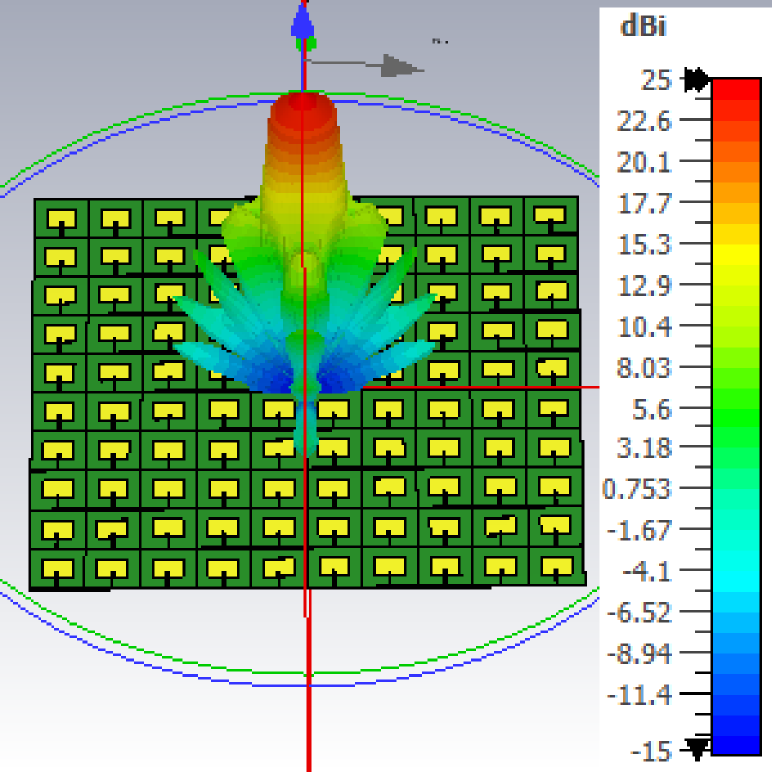
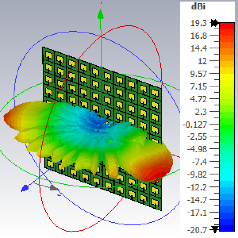
Prior to developing a prototype, we simulated a RIS board with a regular planar antenna array. In our first set of simulations, each antenna element is fed with equal power from an open-ended transmission line that induces a phase delay that is optimized offline to maximize power towards the selected azimuth and elevation angles. Figs. 9(a) and 9(b) show the expected radiation pattern of two different configurations that maximize power towards an elevation of and, respectively, an azimuth of .
On the one hand, we can observe from Fig. 9(a) that the array can achieve a narrow beampattern, with a Half Power Beamwidth (HPBW) equal to , with a gain of dBi in the intended direction, which halves with a 10-degree offset. No back-radiation is expected. On the other hand, Fig. 9(b) shows that a large steering angle of dissipates half the energy towards the opposite direction and drops the power of the beam to dBi.

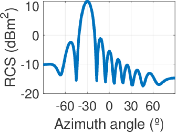
Note however that the power radiated by a RIS comes from an external source that illuminates the surface. In order to simulate this behavior, we generated a plane wave linearly polarized, and measured the resulting Radar Cross Section (RCS). The RCS estimates how much of the incident power at every point of the surface is scattered back to the receiver. Hence, we expect high RCS values in the direction of the main beam and lower in other directions. This is indeed confirmed in Figs. 10(a) and 10(b) for an incidence angle of and , respectively. In both cases, the RIS is configured to reflect the received signal perpendicularly to the incidence angle of the received signal, i.e., the RIS should maximize power in the same direction of the incidence angle, which is confirmed by both figures with a RCS approximately equal to dBsm in the intended direction. This highlights the fact that, in real life scenarios, the angle of arrival must be known to the controller to maximize beamforming gains.
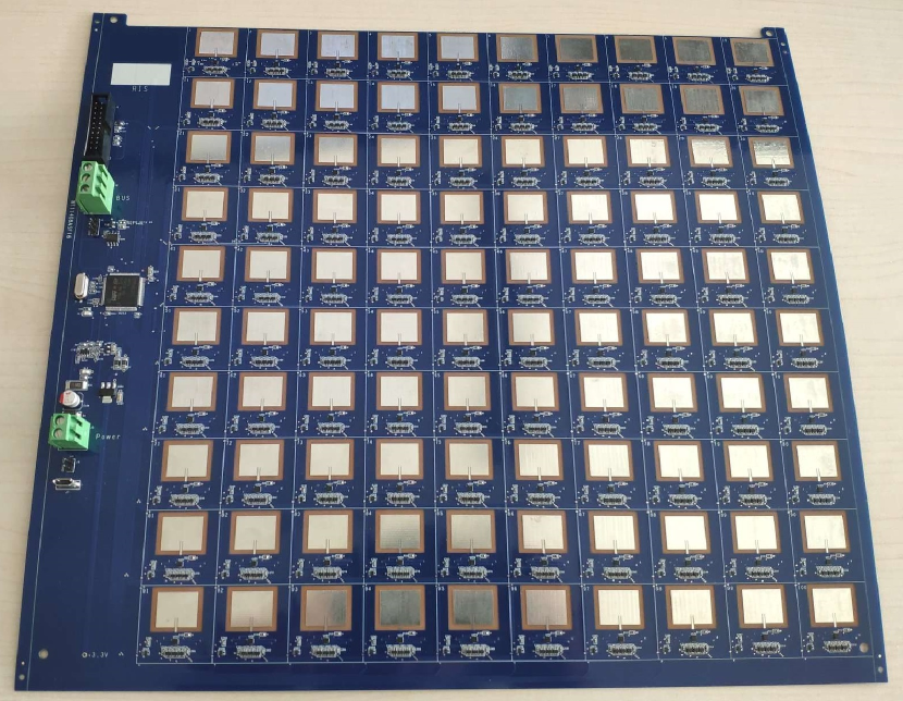
We manufactured 10 boards of 10x10 unit cells each. All the phase and selection buses, which connect each unit cell with an MCU, are built with microstrips. Unit cells are deployed in the PCB layout such that the same inter-cell distance can be maintained across co-located boards. The remaining elements described in §2 (flip-flops, resistors, etc.), are standard components assembled on the PCB. The final printout is shown in Fig. 11(a).
5. Empirical Characterization
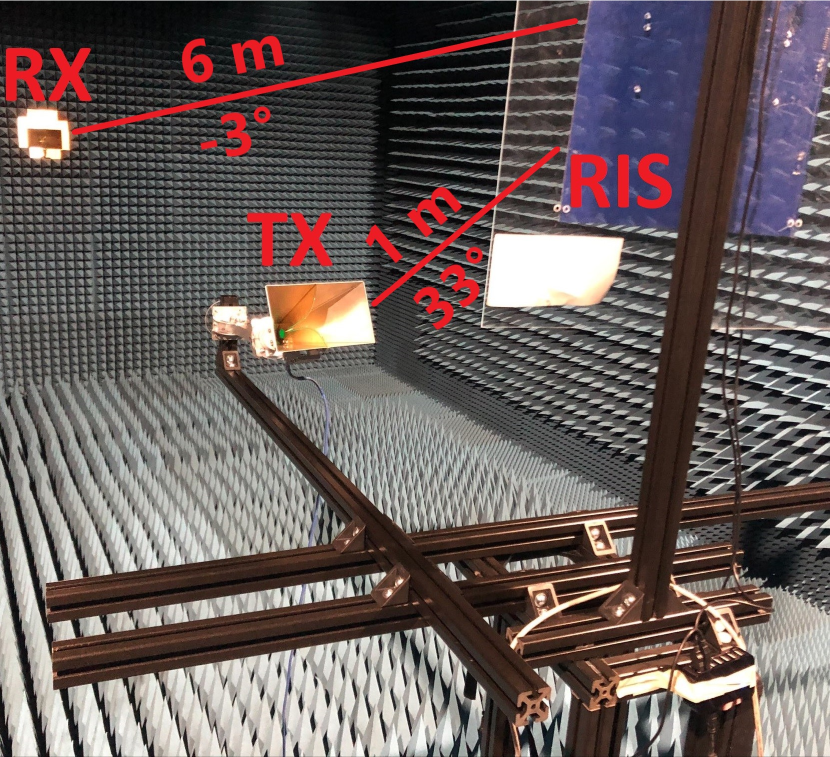
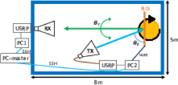
We characterized one of our 10x10 RIS boards in an 8m5m anechoic chamber. Figs. 11(b) and 12 illustrate our testbed. We mounted the board on a turntable controlled remotely from a master PC, which is also used to configure the beamforming parameters of the RIS. We use two software-defined radio devices attached to horn antennas with gain dBi to generate (“TX”) and receive (“RX”) a continuous stream of OFDM QPSK-modulated symbols with 5 MHz of bandwidth and numerology that meets 3GPP LTE requirements. The transmission power of TX is -30 dBm per subcarrier, and we sample the reference signal received power (RSRP) at RX.
The distances RIS-TX and RIS-RX are m and m, respectively. Considering the size of the RIS and its operating frequency, it is hard to guarantee that is larger than the far-field threshold, which is m (Balanis, 2016), where m is the diagonal of the array. Nevertheless, our choice of is larger than the reactive near-field threshold, which is m (Balanis, 2016), and sufficient for our purposes. As shown in Fig. 12, the rotation of the table determines the azimuth angle , and the location of TX determines . Conversely, the elevation angles of RIS-TX and RIS-RX are fixed to and , respectively.
5.1. Codebook characterization
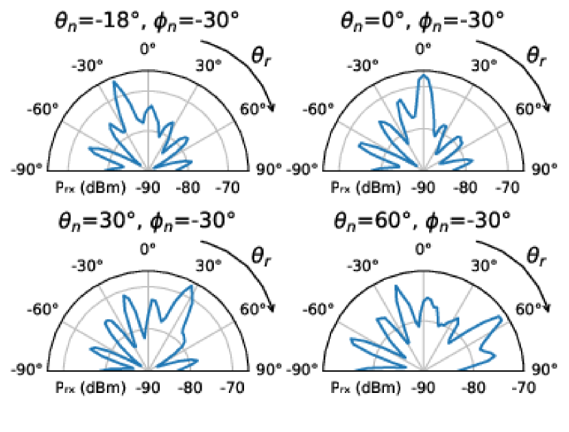
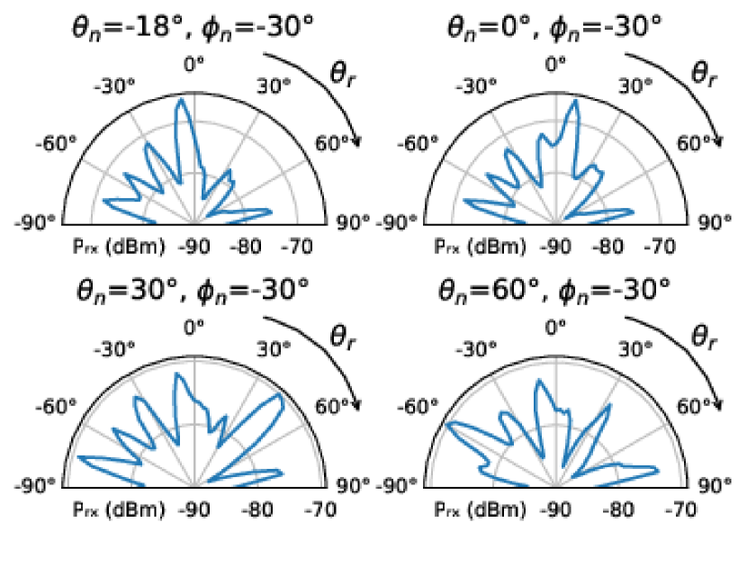
We begin our experimental campaign by characterizing the codebook generated in §3. To this end, we test out all the configurations for a wide range of and for .
For our empirical results, the first observation is that the direction of the main lobe points towards , as intended, for all configurations . These results, hence, validate our prototype for practically all configurations in . Figs. 13 and 14 depict some representative configurations for both settings, respectively. These figures show that the main beam points towards the intended directions. We note, however, that the gain of the main lobe is penalized when we use large steering angles (see, e.g., in both figures), which is expected (Delos et al., 2020). Overall, the power received in the intended direction ranges between dBm (for large steering angles) and dBm (for smaller angles), which give us remarkable beamforming gains between dB and dB over the noise floor.
Using the radar range equation in (Balanis, 2016), the peak RCS can be calculated as dBm2. Moreover, the HPBW is in average around for all beampatterns. Both results are in line with our simulations in §4.4.
5.2. Scalability analysis


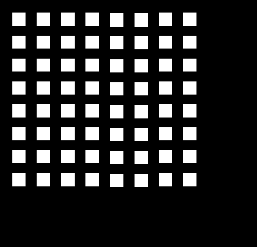
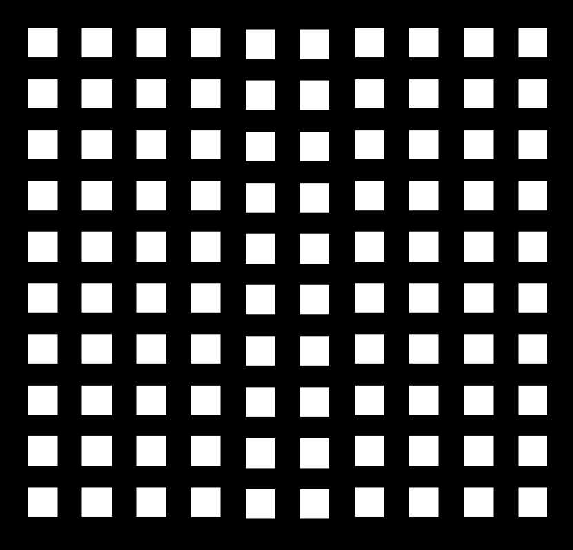
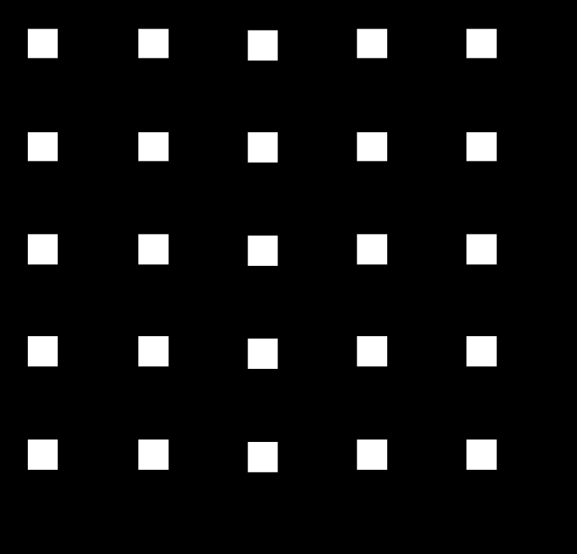
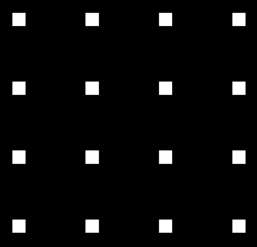
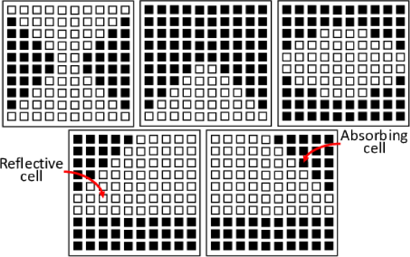
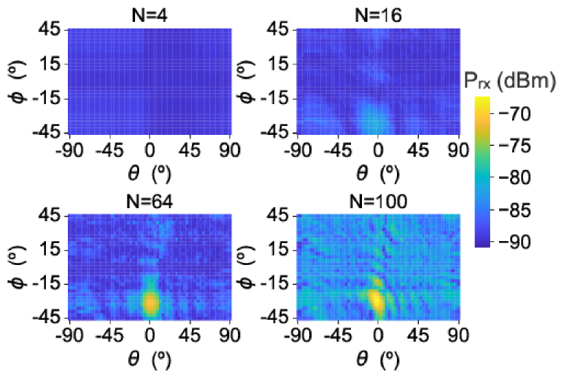
To assess scalability, we analyze the beamforming gain of our RIS for a variable number of unit cells. To this goal, we take advantage of the absorption state available in our design for each cell, and produce virtual RISs with different sizes by setting the activation patterns shown in Figs. 15(a) to 15(d). For every virtual RIS, we re-optimized its codebook to account for its effective size and inter-cell spacing.
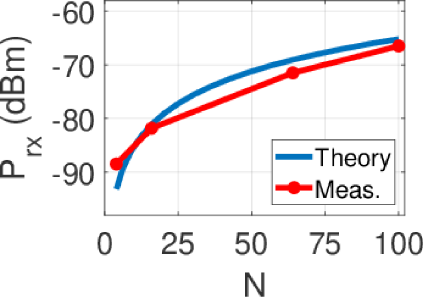
To ease the analysis, we now fix and measure the power received for every configuration . The results are shown in Fig. 16, which represent the measured power with a color range for every combination of (x-axis) and (y-axis) from , and for . From these plots, we can observe how the main beam becomes sharper and carries more power as we increase . With (top left plot), no configuration produces a distinguishable beam, which renders a 2x2 RIS ineffective. For the rest, we note a growing amount of power in the intended direction, respectively, equal to dBm (), dBm (), and dBm (all cells are activated). This behavior is expected: Fig. 19 depicts in red the power observed at RX with the optimal configuration as a function of , and compares that with the mathematical model in (Tang et al., 2021) (see eq. (5) therein) represented in blue. Both results are remarkably close to each other, which validates the ability of our approach to effectively create virtual surfaces with different shapes.
5.3. Other activation patterns
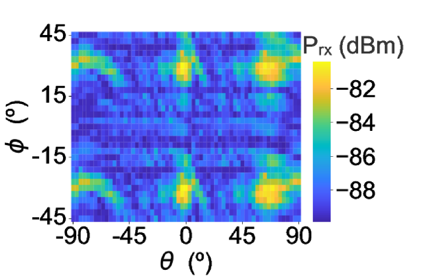
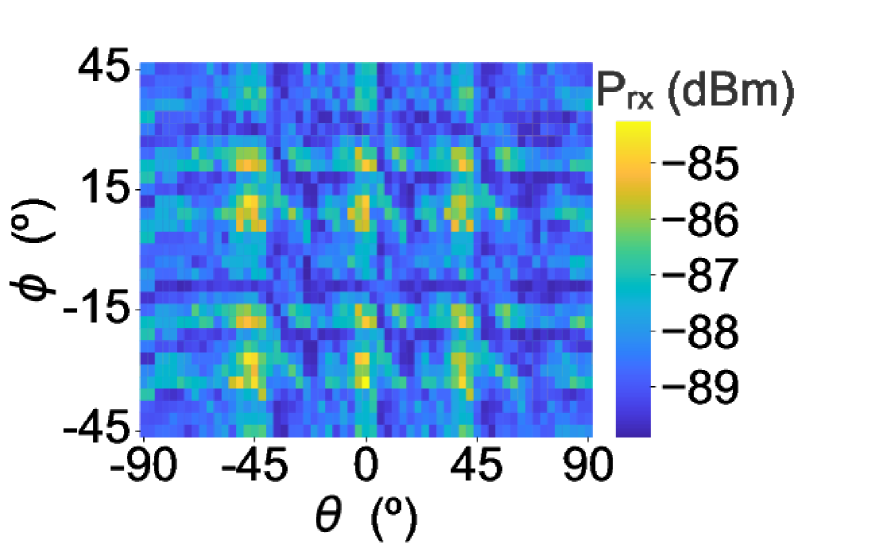
To conclude our characterization, we study the performance of our RIS prototype when the inter-cell distance differs from (shown in Fig. 16 for ). Like before, we calculated new optimized codebooks for , and plot in Fig. 17 the power received at RX for each configuration . We do this for both activation patterns depicted in Fig. 15(e) (“off2”) and 15(f) (“off3”), for and , respectively.
By changing , we also change the density of active cells per board, for (Fig. 17(a)) and for (Fig. 17(b)). As shown earlier, this has a cost in terms of beamforming gains that is evidenced also in Fig. 17: the maximum power is dBm and dBm for the two cases, respectively. Both plots reveal the presence of grating lobes, which are symmetrical beams that are denser for larger values. These effects are well understood in the literature of antenna design and their distance can be estimated using our model in §3. The figure depicts with red circles the expected location of these lobes, which match our measurements remarkably well. This further validates our design to effectively modify the shape of the RIS to the requirements of any given use case.
6. Reproducibility
To conclude our paper, we provide some final remarks that shall help researchers in the RIS domain build on our results (dataset) and/or reproduce our RIS prototype.
For starters, we publicly release the dataset111We will publish the dataset upon the paper acceptance. we have generated during our empirical characterization in §5, which aggregates a total number of power samples. This data can help other researchers study RIS-related problems without the need of building a prototype.
Next, we report the costs associated for building our prototype. For this purpose, we have used prices publicly available. There are three sources of cost to manufacture each board: () PCB production (including the patch antenna and the microstrips for the delay lines and the buses); () additional electronic components (including RF switches, MCU, resistors, flip-flops, AND gates, etc.); and () assembly all components onto the PCB.
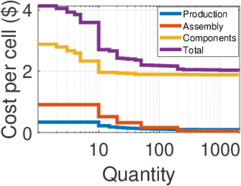
According to PCBWay (PCBWay, [n. d.]), producing 10 PCB boards, as specified in our design, costs $0.22 per unit cell; but it drops to $0.11 and $0.09 when the production scales up by 20x and 100x, respectively. Concerning additional electronic components, each 10x10 board bears 300 flip-flops, 100 AND gates, 100 RF switches, and 1 MCU. According to Digikey.de, the cost boils down to $1.88 per unit cell when purchasing a batch of 1000 of such boards. The assembly process, according to PCBWay, scales down from $0.51 to $0.05 per cell when we scale up the number of boards from 10 to 1000 10x10-RISs. Fig. 19 depicts how these costs (normalized per unit cell) evolve with the manufacturing scale.
7. Conclusion
Reconfigurable Intelligent Surfaces (RISs) can become a major densification solution for future mobile systems. We designed, prototyped and characterized an RF switch-based RIS that met our defined requirements in terms of RF steering, reconfigurability, energy efficiency, and cost. Throughout the paper, we reported on our learnings along with the related experiments. These learnings ranged from our experience bridging theory and empirical findings (e.g., unexpected sensitivity to certain model parameters) to practical considerations (e.g., costs and hardware constrains). As a result, our contributions can be used by the research community to: () build realistic RF switch-based RIS models, () leverage on the dataset provided to further study related challenges, () reproduce our RIS prototype for research purposes, and () estimate the deployment costs at scale.
References
- (1)
- Albanese et al. (2022) Antonio Albanese et al. 2022. MARISA: A Self-configuring Metasurfaces Absorption and Reflection Solution Towards 6G. In IEEE INFOCOM 2022 - IEEE Conference on Computer Communications.
- Analog Devices (2009) Analog Devices. 2009. Microstrip and Stripline Design: MT-094 tutorial. https://www.analog.com/media/en/training-seminars/tutorials/MT-094.pdf. (2009). Accessed: 2022-03-01.
- Arun and Balakrishnan (2020) Venkat Arun and Hari Balakrishnan. 2020. RFocus: Beamforming using thousands of passive antennas. In USENIX NSDI.
- Balanis (2016) Constantine A Balanis. 2016. Antenna theory: analysis and design. John wiley & sons.
- Basar et al. (2019) Ertugrul Basar et al. 2019. Wireless communications through reconfigurable intelligent surfaces. IEEE access 7 (2019), 116753–116773.
- Dai et al. (2020) Linglong Dai et al. 2020. Reconfigurable intelligent surface-based wireless communications: Antenna design, prototyping, and experimental results. IEEE Access 8 (2020), 45913–45923.
- Dassault Systèmes (2022) Dassault Systèmes. 2022. CST Studio Suite: Electromagnetic field simulation software. https://www.3ds.com/products-services/simulia/products/cst-studio-suite/. (2022). Accessed: 2022-03-01.
- Delos et al. (2020) Peter Delos, Bob Broughton, and Jon Kraft. 2020. Phased Array Antenna Patterns—Part 2: Grating Lobes and Beam Squint. 26 Phased Array Antenna Patterns—Series (2020), 39.
- Dunna et al. (2020) Manideep Dunna et al. 2020. ScatterMIMO: Enabling virtual MIMO with smart surfaces. In ACM MobiCom.
- Fara et al. (2021) Romain Fara et al. 2021. A Prototype of Reconfigurable Intelligent Surface with Continuous Control of the Reflection Phase. arXiv preprint arXiv:2105.11862 (2021).
- Hu et al. (2020) Jingzhi Hu et al. 2020. Reconfigurable Intelligent Surface Based RF Sensing: Design, Optimization, and Implementation. IEEE Journal on Selected Areas in Communications 38, 11 (2020), 2700–2716.
- Mir et al. (2021) Muhammad Sarmad Mir et al. 2021. PassiveLiFi: rethinking LiFi for low-power and long range RF backscatter. In ACM MobiCom.
- Mursia et al. (2021) Placido Mursia et al. 2021. RISMA: Reconfigurable Intelligent Surfaces Enabling Beamforming for IoT Massive Access. IEEE Journal on Selected Areas in Communications 39, 4 (2021), 1072–1085.
- Pan et al. (2021) Cunhua Pan et al. 2021. Reconfigurable Intelligent Surfaces for 6G Systems: Principles, Applications, and Research Directions. IEEE Communications Magazine 59, 6 (2021), 14–20.
- Pandey (2019) Anil Pandey. 2019. Practical microstrip and printed antenna design. Artech House.
- PCBWay ([n. d.]) PCBWay. [n. d.]. PCB prototype and fabrication. https://www.pcbway.com. ([n. d.]).
- Skyworks Solutions, Inc (2019) Skyworks Solutions, Inc. 2019. SKY13418-485LF: 0.1 to 6.0 GHz SP8T Antenna Switch. https://www.skyworksinc.com/-/media/SkyWorks/Documents/Products/701-800/SKY13418_485LF_201712F.pdf. (2019). Accessed: 2022-03-01.
- STMicroelectronics (2021) STMicroelectronics. 2021. STM32L071V8: Ultra-low-power Arm Cortex-M0+ MCU with 64-Kbytes of Flash memory, 32 MHz CPU . https://www.st.com/en/microcontrollers-microprocessors/stm32l071v8.html. (2021). Accessed: 2022-03-01.
- Tan et al. (2018) Xin Tan, Zhi Sun, Dimitrios Koutsonikolas, and Josep M Jornet. 2018. Enabling indoor mobile millimeter-wave networks based on smart reflect-arrays. In IEEE INFOCOM 2018-IEEE Conference on Computer Communications. IEEE, 270–278.
- Tang et al. (2021) Wankai Tang et al. 2021. Wireless Communications With Reconfigurable Intelligent Surface: Path Loss Modeling and Experimental Measurement. IEEE Transactions on Wireless Communications 20, 1 (2021), 421–439. https://doi.org/10.1109/TWC.2020.3024887
- Trichopoulos et al. (2021) Georgios Trichopoulos et al. 2021. Design and Evaluation of Reconfigurable Intelligent Surfaces in Real-World Environment. arXiv preprint arXiv:2109.07763 (2021).
- Wu et al. (2018) Qingqing Wu et al. 2018. Intelligent Reflecting Surface Enhanced Wireless Network: Joint Active and Passive Beamforming Design. IEEE Transactions on Wireless Communications 18, 11 (2018), 5394–5409.
- Yang et al. (2022) Zhaohui Yang et al. 2022. Energy-Efficient Wireless Communications With Distributed Reconfigurable Intelligent Surfaces. IEEE Transactions on Wireless Communications 21, 1 (2022), 665–679.
- Yezhen et al. (2020) Li Yezhen et al. 2020. A Novel 28 GHz Phased Array Antenna for 5G Mobile Communications. ZTE Communications 18, 3 (2020), 20–25.