Memristive and tunneling effects in 3D interconnected silver nanowires
Abstract
Due to their memristive properties nanowire networks are very promising for neuromorphic computing applications.
Indeed, the resistance of such systems can evolve with the input voltage or current as it confers a synaptic behaviour to the device.
Here, we propose a network of silver nanowires (Ag-NWs) which are grown in a nanopourous membrane with interconnected nanopores by electrodeposition.
This bottom-up approach fabrication method gives a conducting network with a 3D architecture and a high density of Ag-NWs.
The resulting 3D interconnected Ag-NW network exhibits a high initial resistance as well as a memristive behavior.
It is expected to arise from the creation and the destruction of conducting silver filaments inside the Ag-NW network.
Moreover, after several cycles of measurement, the resistance of the network switches from a high resistance regime, in the range, with a tunnel conduction to a low resistance regime, in the range.
A limitation of current computer architecture is the separation between the memory and the processing unit which leads to the von Neumann bottleneck. To go beyond this bottleneck, a new field named neuromorphic computing1 has emerged which takes inspirations from the brain to be more efficient. Indeed, in the brain, the synapses, which act as memory, and the neurons, which act as processing units, are distributed and the neurons are strongly interconnected through the synapses resulting in a highly parallel architecture. The complexity of the brain, its high number of interconnections, which can be recurrent, inspire the fabrication of neuromorphic devices2. They are based on various physical principles like spintronics3, optics4 or memristive devices5, 6, 7, 8.
Memristors were theorised by Chua in 1971 and described as the missing component linking charge and flux9. In 2008, Strukov et al10 showed that some nanodevices exhibiting a non-linear hysteretic curve are in fact memristive devices. This phenomena was previously observed in memory based on resistive switching 11 and memristor were proposed later as neuromorphic synapses5. Resistive switching arises from different phenomena11, 12 including the formation and destruction of conductive filaments (CFs) from the migration of metallic ions of Cu13 or Ag14 for example. Atomic switches based on CF are convenient as they can be integrated in a crossbar structure 14. However, in the brain, neurons are highly interconnected by synapses and the connections can be recurrent which leads to a much more complex structure compared to crossbar architecture. Thus, nanowire networks and especially silver nanowire (Ag-NW) networks15 seem to be good candidates for neuromorphic computing as they have both numerous interconnections and memristive properties. In addition, Ag-NWs can be used for transparent electronics16, have a low electrical resistivity17, and are easily fabricated by different methods6, 18, 19.
Several fabrication processes are used to fabricate Ag-NW network like growing Ag-NWs from Cu seeds6 or with a polyol synthesis20 and a polyvinylpyrrolidone (PVP) coating18, 7, 8, 21 (more fabrication processes are detailed in this review19). PVP coated Ag-NWs can exhibit different density of Ag-NWs in the sample8 as well as a larger resistance because of the PVP coating18. Several post-treatments can be used to increase the connections between Ag-NWs including thermal annealing, mechanical pressing and other techniques17, 18. On the contrary, one can use post-treatments to increase the resistance of the network and create opportunities for the creation of Ag CFs so that the network exhibits a memristive behavior. It can be done either thanks to the encapsulation of the Ag NWs in an insulating shell like PVP18, 8, 21 where conductive filaments grow across the PVP insulating layer21 or by fragmenting the Ag-NWs with an UV/ozone irradiation followed by an annealing7.
In this work, we propose a memristive device made of three-dimensional (3D) interconnected Ag-NWs. Those are deposited inside a nanoporous membrane which allows a bottom-up fabrication of a random but ordered NW network with a high number of interconnections22.
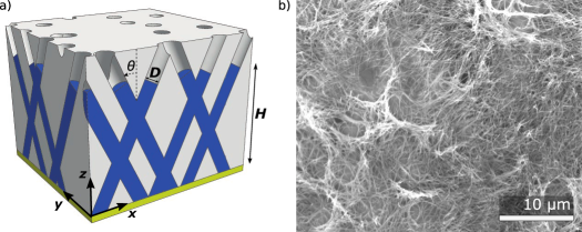
An electrochemical deposition in ion track nanoporous polycarbonate (PC) membrane was employed to produce 3D interconnected Ag-NWs as shown schematically in fig.1(a). The PC nanoporous membrane with interconnected nanopores has been fabricated by exposing a -thick PC film to a two-step irradiation process. The topology of the membrane was defined by exposing the film to a first irradiation step at two fixed angles of and with respect to the normal axis of the film plane. In pratice, the angles are between and . After rotating the PC film in the plane by , the second irradiation step took place at the same fixed angular irradiation flux to finally form a 3D nanoporous network. The diameter of the latent tracks was enlarged by following a previously reported protocol23 to obtain a membrane with an average pore diameter of 30 nm and a volumetric porosity of about 0.4%. Next, the PC templates were coated on one side using an e-beam evaporator with a metallic Cr (3 nm)/Au (250 nm) bilayer to serve as a cathode during the electrochemical deposition. The Ag-NWs were fabricated by electrodeposition using a silver-cyanide-based commercial electrolyte (Silver-Bright-100, Metaken GmbH) in a two-electrode configuration at room temperature by applying a constant potential of -1.5 V versus a double-junction Ag/AgCl reference electrode and a platinum strip used as a counter electrode. The reaction is the following:
| (1) |
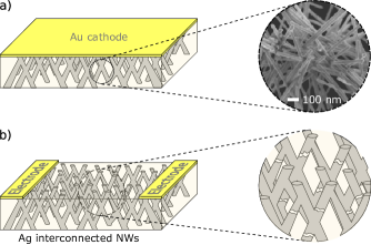
After the silver electrodeposition process, the network height is approximately . A schematic view of the sample is presented in fig.1(a). The morphology of the interconnected Ag-NW network was characterized using a field-emission scanning electron microscope (FE-SEM). For the electron microscopy analysis, the PC template was removed by chemical dissolution using dichloromethane from Sigma-Aldrich. As the network porosity is low, the network collapses once the membrane is completely removed as shown on the SEM image in fig. 1(b). A scheme of the Ag-NWs encapsulated in the membrane with the Au cathode is presented in fig. 2(a) while its inset shows a closer and tilted view of SEM image of the 3D interconnected Ag-NW network. As it can be seen, the Ag-NW network has a complex interconnected structure.
The 3D structure presents a high number of interconnections with the possibility of recurrent connections with the advantages of NWs with a regular diameter and length. The number of interconnections is estimated numerically and gives 5.5 1.0 interconnections per . For the network height, the density is around 107 interconnections per which is one order of magnitude greater than this recent structure24. The number of interconnection is easily adapted by adjusting the NWs diameter as well as the membrane porosity. It is interesting to note that the interconnections between Ag NWs share different portion of volume from none (i.e. no crossing) to a complete crossing.
Previously reported 3D interconnected NW network25 with NWs made of Ni with a diameter of 80 nm and a volumetric porosity of 3% have reached resistance as low as . To increase the resistance of the 3D interconnected Ag-NW network and see a memristive behavior, the Ag-NWs needs to be damaged. This is achieved during the etching process where the cathode is partially removed to create a two electrodes device for electrical measurements26 while insulating domains are created in the network (see fig. 2(b)). Indeed, the plasma etching also led to some heating of the polymer membrane which is expected to generate gaps and holes in the sparse network of Ag-NW resulting in a sample with a high initial resistance. The resistance of the 3D interconnected Ag-NW network is then in the range and above. The etching process is thus considered as a functionalizing step.
This fabrication process allows to produce NWs below the lithography limit with numerous interconnections and a complexity beyond crossbar architecture as well as providing an easy scale-up of the system by simply increasing its surface. As the Ag-NWs are already interconnected, the membrane is not dissolved at the end of the fabrication. Thus, the network has an enhanced solidity, is flexible27 and is protected against oxidation. In addition, the randomness needed for neuromorphic application is conserved due to the random location of nanopores in the membrane, the variety of crossing types and the functionalizing step. This method is low-cost, reliable and both diameter and density of Ag-NWs can be easily tuned.
The measured sample is about 5 mm long and 1 mm wide, and the electrical contacts were directly made by silver paint. The curves of the Ag-NWs were obtained using a Keithley 617 electrometer. All measurements are made at room temperature and tests were made to discard any electrical conduction via the PC membrane to ensure a complete conduction through the Ag-NWs and their interconnections only. First, an cycle is repeated several times with a voltage ramp increasing from 0 V to 100 V before decreasing back to with a time step of 1 V/s (see Fig. 3). The data are denoised thanks to a digital wavelet transform28 and the same offset is added to each sweep to ensure a positive current. Four consecutive cycles are plotted in Fig. 3). One can see the typical behavior of a memristive system with a pinched hysteresis for all measurements. Similar results were obtain in bulk silver nanowire–polystyrene composites15 with an applied voltage ramp up to 160 V and with PVP-coated Ag-NW network 29 for a threshold voltage below 2V. We expect that the memristive behaviour arises from the creation of field-induced Ag CF in the holes and gaps created during the plasma etching when the voltage increases. However, when the voltage decreases, the new filaments break due to Rayleigh instability30 and, hence, the resistance increases. Indeed, the atoms in the filaments are less stable than the atoms in bulk nanowires, thus the creation of silver filaments is volatile.
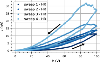
For each cycle, there is a local minimum resistance. Their values are 8.40 0.02 , 7.11 0.04 , 4.84 0.02 and 2.73 0.02 , respectively. One can notice that the local minimum resistance decreases with each consecutive cycle. Even with a voltage ramp reaching a high voltage (100 V), as the current flowing in the device is in the nA range, the maximal power reach for each sweep is respectively , , and . This device is then resilient to high input voltage with a moderate power consumption.
For the first sweep, a change of the conduction occurs when a threshold voltage is exceeded which leads to a strong current increase. Below this threshold, the increase of the current with the voltage is much smaller. This can be explained by the switching between direct tunneling at low voltage and field emission at high voltage as a Fowler-Nordheim plot suggests 31 (see Fig. 4(b)). Similar results have been reported with another type of Ag-NW network7. We suppose that the tunnel conduction arises when nanowires are separated by an empty zone or gap acting like an insulating barrier which appears during the etching of the cathode.
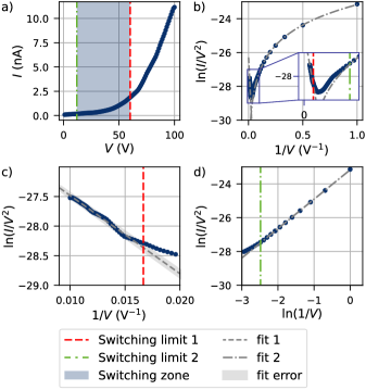
In order to have an estimation of the switching zone between these two regimes, a linear fitting is performed on a selection of data for both field emission and direct tunneling (respectively "fit 1" and "fit 2" on Fig. 4). For the field emission, a linear dependence is shown when is plotted as a function of as it appears in Fig. 4(c). The direct tunneling exhibits a linear dependence when is plotted as a function of as shown in Fig. 4(d). An error is extracted from "fit 1" (resp. "fit 2") and the switching limits are determined as the first (resp. last) value outside the fitting error range. The error of "fit 2" is small and is hardly seen in Fig. 4(d). These two switching limits are 12 and 60 V for the direct tunneling and field emission respectively. The switching of the tunneling conduction arises from a change of the tunneling barrier shape from a rectangular barrier to a triangular barrier31 which enhances the probability of tunneling.
We repeatedly measured this sample with cycles, until its resistance dropped in the range and below. This new regime is called low resistance regime (LR) due to the decrease of the minimum resistance by a factor of about 47,000.
After several repeated cycles, we suppose that some filaments present an extended lifetime leading to a strong decrease of the resistance.
A similar behaviour was reported by Avizienis et al6.
Several measurements are made in the low resistance regime and two consecutive cycles are reported in Fig. 5. The data are denoised in two steps. First, outliers above are suppressed and replaced thanks to an interpolation. Then, the data are denoised with a digital wavelet transform28. As seen in Fig. 5, a different memristive behavior is observed compared to the high resistance regime.
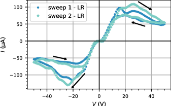
The voltage ramp starts at 0 V, increases to 50 V before decreasing to -50 V and returning to 0 V. The curves show several interesting behaviors. At first, the current increases with the voltage for V until V depending on the sweep. Then, the current decreases while the voltage continues to increase until V is reached. Then, the current increases while the voltage decreases until 15-20 V and finally, the current decreases with the voltage until V. The same repeats in a symmetric way when the voltage goes down to -50 V and back to 0 V.
This induces that during the first half of the sweep, a local maximum and two local minima of resistance are reached.
The corresponding resistances are given in Table 1 before being averaged.
The resulting averaged minimum resistance is while the following averaged maximum resistance is obtained: .
There is a factor six between the minimum and the maximum averaged resistance in the first-half of the sweeps.
Similar results were obtained in the second half of the sweeps with and .
In this low resistance regime, the minimum resistances are in the range, with a voltage threshold in the order of 2 V.
| Sweep 1 - LR | Sweep 2 - LR | |
|---|---|---|
| 0.150 at 13 V | 0.168 at 15 V | |
| 1.007 at 50 V | 0.923 at 50 V | |
| 0.157 at 10 V | 0.178 at 9 V |
In conclusion, we reported a 3D interconnected Ag-NW network with a simple two step fabrication process composed of a template-assisted electrodeposition and an etching leading to a highly interconnected network. The latter has a double function as it both damages the Ag NWs creating holes and gaps were Ag CF can grow, giving rise to memristive properties to the 3D interconnected Ag NW network, and defines electrode pads for electrical connection. In the future, the etching pattern will be tuned from a basic two electrodes design to a more elaborate pattern with numerous input/output pads. The resulting NWs are highly ordered and encapsulated in a 3D nanoporous polymer film. The 3D architecture allows to have 5.5 1.0 108 interconnections per with an increased complexity as the interconnections are random with a variety of crossing type. Two resistance regimes are measured with different resistance range: in the range and above for the high resistance regime and in the range and below for the low resistance regime. A tunneling conduction arises in the high resistance regime and both high and low resistance regimes exhibit a memristive behavior. The presented 3D interconnected Ag-NW network could be used for neuromorphic applications due to its memristive properties and more precisely for reservoir computing in a similar way as these recent studies32, 21. In addition, the high density of interconnections will be exploited to train multiple learning process on the same device as numerous pathway are expected to growth in the Ag-NWs network29. Thus, it is a promising device for future application in neuromorphic computing.
Author’s contribution
F.A.A. and L.P. designed the study. N.M., L.P., and P.V.V. fabricated the samples. F.A.A. conceived and designed the experimental measurement setup and the analysis. F.A.A., C.C. and S.d.W. collected the data and performed the analysis. C.C. wrote the core of the manuscript and all the other co-authors contributed to it.
F.A.A. is a Research Associate of the F.R.S.-FNRS. S.d.W. aknowledges the Walloon Region and UCLouvain for FSR financial support. N.M. acknowledges the Research Science Foundation of Belgium (F.R.S.-FNRS) for financial support (FRIA grant). The authors would like to thank Dr. E. Ferain and the it4ip Company for supplying polycarbonate membranes.
References
- Indiveri and Horiuchi 2011 Indiveri, G.; Horiuchi, T. K. Frontiers in neuromorphic engineering. Frontiers in neuroscience 2011, 5, 118, DOI: 10.3389/fnins.2011.00118
- Zhu et al. 2020 Zhu, J.; Zhang, T.; Yang, Y.; Huang, R. A comprehensive review on emerging artificial neuromorphic devices. Applied Physics Reviews 2020, 7, 011312, DOI: 10.1063/1.5118217
- Grollier et al. 2020 Grollier, J.; Querlioz, D.; Camsari, K.; Everschor-Sitte, K.; Fukami, S.; Stiles, M. D. Neuromorphic spintronics. Nature electronics 2020, 3, 360–370, DOI: 10.1038/s41928-019-0360-9
- Shastri et al. 2021 Shastri, B. J.; Tait, A. N.; de Lima, T. F.; Pernice, W. H.; Bhaskaran, H.; Wright, C. D.; Prucnal, P. R. Photonics for artificial intelligence and neuromorphic computing. Nature Photonics 2021, 15, 102–114, DOI: 10.1038/s41566-020-00754-y
- Jo et al. 2010 Jo, S. H.; Chang, T.; Ebong, I.; Bhadviya, B. B.; Mazumder, P.; Lu, W. Nanoscale memristor device as synapse in neuromorphic systems. Nano letters 2010, 10, 1297–1301, DOI: 10.1021/nl904092h
- Avizienis et al. 2012 Avizienis, A. V.; Sillin, H. O.; Martin-Olmos, C.; Shieh, H. H.; Aono, M.; Stieg, A. Z.; Gimzewski, J. K. Neuromorphic atomic switch networks. PLoS ONE 2012, DOI: 10.1371/journal.pone.0042772
- Wan et al. 2018 Wan, T.; Pan, Y.; Du, H.; Qu, B.; Yi, J.; Chu, D. Threshold switching induced by controllable fragmentation in silver nanowire networks. ACS applied materials & interfaces 2018, 10, 2716–2724, DOI: 10.1021/acsami.7b16142
- Diaz-Alvarez et al. 2019 Diaz-Alvarez, A.; Higuchi, R.; Sanz-Leon, P.; Marcus, I.; Shingaya, Y.; Stieg, A. Z.; Gimzewski, J. K.; Kuncic, Z.; Nakayama, T. Emergent dynamics of neuromorphic nanowire networks. Scientific reports 2019, 9, 1–13, DOI: 10.1038/s41598-019-51330-6
- Chua 1971 Chua, L. Memristor-the missing circuit element. IEEE Transactions on circuit theory 1971, 18, 507–519, DOI: 10.1109/TCT.1971.1083337
- Strukov et al. 2008 Strukov, D. B.; Snider, G. S.; Stewart, D. R.; Williams, R. S. The missing memristor found. nature 2008, 453, 80–83, DOI: 10.1038/nature06932
- Waser and Aono 2010 Waser, R.; Aono, M. Nanoscience And Technology: A Collection of Reviews from Nature Journals; World Scientific, 2010; pp 158–165, DOI: 10.1142/9789814287005_0016
- Sawa 2008 Sawa, A. Resistive switching in transition metal oxides. Materials today 2008, 11, 28–36, DOI: 10.1016/S1369-7021(08)70119-6
- Banno et al. 2006 Banno, N.; Sakamoto, T.; Hasegawa, T.; Terabe, K.; Aono, M. Effect of ion diffusion on switching voltage of solid-electrolyte nanometer switch. Japanese journal of applied physics 2006, 45, 3666, DOI: 10.1143/jjap.45.3666
- Terabe et al. 2005 Terabe, K.; Hasegawa, T.; Nakayama, T.; Aono, M. Quantized conductance atomic switch. Nature 2005, 433, 47–50, DOI: 10.1038/nature03190
- White et al. 2011 White, S. I.; Vora, P. M.; Kikkawa, J. M.; Winey, K. I. Resistive switching in bulk silver nanowire–polystyrene composites. Advanced Functional Materials 2011, 21, 233–240, DOI: 10.1002/adfm.201001383
- Hu et al. 2010 Hu, L.; Kim, H. S.; Lee, J.-Y.; Peumans, P.; Cui, Y. Scalable coating and properties of transparent, flexible, silver nanowire electrodes. ACS nano 2010, 4, 2955–2963, DOI: 10.1021/nn1005232
- Bellew et al. 2015 Bellew, A. T.; Manning, H. G.; Gomes da Rocha, C.; Ferreira, M. S.; Boland, J. J. Resistance of single Ag nanowire junctions and their role in the conductivity of nanowire networks. ACS nano 2015, 9, 11422–11429, DOI: 10.1021/acsnano.5b05469
- Du et al. 2017 Du, H.; Wan, T.; Qu, B.; Cao, F.; Lin, Q.; Chen, N.; Lin, X.; Chu, D. Engineering silver nanowire networks: from transparent electrodes to resistive switching devices. ACS applied materials & interfaces 2017, 9, 20762–20770, DOI: 10.1021/acsami.7b04839
- Milano et al. 2019 Milano, G.; Porro, S.; Valov, I.; Ricciardi, C. Recent developments and perspectives for memristive devices based on metal oxide nanowires. Advanced Electronic Materials 2019, 5, 1800909, DOI: 10.1002/aelm.201800909
- Coskun et al. 2011 Coskun, S.; Aksoy, B.; Unalan, H. E. Polyol synthesis of silver nanowires: an extensive parametric study. Crystal Growth & Design 2011, 11, 4963–4969, DOI: 10.1021/cg200874g
- Milano et al. 2021 Milano, G.; Pedretti, G.; Montano, K.; Ricci, S.; Hashemkhani, S.; Boarino, L.; Ielmini, D.; Ricciardi, C. In materia reservoir computing with a fully memristive architecture based on self-organizing nanowire networks. Nature Materials 2021, 1–8, DOI: 10.1038/s41563-021-01099-9
- Rauber et al. 2011 Rauber, M.; Alber, I.; Müller, S.; Neumann, R.; Picht, O.; Roth, C.; Schökel, A.; Toimil-Molares, M. E.; Ensinger, W. Highly-ordered supportless three-dimensional nanowire networks with tunable complexity and interwire connectivity for device integration. Nano letters 2011, 11, 2304–2310, DOI: 10.1021/nl2005516
- Ferain and Legras 2003 Ferain, E.; Legras, R. Track-etch templates designed for micro-and nanofabrication. Nuclear Instruments and Methods in Physics Research Section B: Beam Interactions with Materials and Atoms 2003, 208, 115–122, DOI: 10.1016/S0168-583X(03)00637-2
- Milano et al. 2020 Milano, G.; Pedretti, G.; Fretto, M.; Boarino, L.; Benfenati, F.; Ielmini, D.; Valov, I.; Ricciardi, C. Brain-inspired structural plasticity through reweighting and rewiring in multi-terminal self-organizing memristive nanowire networks. Advanced Intelligent Systems 2020, 2, 2000096, DOI: 10.1002/aisy.202000096
- da Câmara Santa Clara Gomes et al. 2019 da Câmara Santa Clara Gomes, T.; Marchal, N.; Abreu Araujo, F.; Piraux, L. Tunable magnetoresistance and thermopower in interconnected NiCr and CoCr nanowire networks. Applied Physics Letters 2019, 115, 242402, DOI: 10.1063/1.5130718
- da Câmara Santa Clara Gomes et al. 2019 da Câmara Santa Clara Gomes, T.; Abreu Araujo, F.; Piraux, L. Making flexible spin caloritronic devices with interconnected nanowire networks. Science advances 2019, 5, eaav2782, DOI: 10.1126/sciadv.aav2782
- da Câmara Santa Clara Gomes et al. 2021 da Câmara Santa Clara Gomes, T.; Marchal, N.; Abreu Araujo, F.; Velázquez Galván, Y.; de la Torre Medina, J.; Piraux, L. Magneto-Transport in Flexible 3D Networks Made of Interconnected Magnetic Nanowires and Nanotubes. Nanomaterials 2021, 11, 221, DOI: 10.3390/nano11010221
- Lee et al. 2019 Lee, G. R.; Gommers, R.; Waselewski, F.; Wohlfahrt, K.; O’Leary, A. PyWavelets: A Python package for wavelet analysis. Journal of Open Source Software 2019, 4, 1237, DOI: 10.21105/joss.01237
- Diaz-Alvarez et al. 2020 Diaz-Alvarez, A.; Higuchi, R.; Li, Q.; Shingaya, Y.; Nakayama, T. Associative routing through neuromorphic nanowire networks. AIP Advances 2020, 10, 025134, DOI: 10.1063/1.5140579
- Wang et al. 2019 Wang, W.; Wang, M.; Ambrosi, E.; Bricalli, A.; Laudato, M.; Sun, Z.; Chen, X.; Ielmini, D. Surface diffusion-limited lifetime of silver and copper nanofilaments in resistive switching devices. Nature communications 2019, 10, 1–9, DOI: 10.1038/s41467-018-07979-0
- Araidai and Tsukada 2010 Araidai, M.; Tsukada, M. Theoretical calculations of electron transport in molecular junctions: Inflection behavior in Fowler-Nordheim plot and its origin. Physical Review B 2010, 81, 235114, DOI: 10.1103/PhysRevB.81.235114
- Kuncic et al. 2020 Kuncic, Z.; Kavehei, O.; Zhu, R.; Loeffler, A.; Fu, K.; Hochstetter, J.; Li, M.; Shine, J. M.; Diaz-Alvarez, A.; Stieg, A., et al. Neuromorphic information processing with nanowire networks. 2020 IEEE International Symposium on Circuits and Systems (ISCAS). 2020; pp 1–5, DOI: 10.1109/ISCAS45731.2020.9181034