Evidence of the disorder-independent electron-phonon scattering time in thin NbN films
Abstract
We report on experimental study of the effect of disorder on electronic parameters and inelastic scattering mechanisms in ultrathin superconducting NbN films, which are commonly used in single-photon detectors. An increase in disorder in the studied 2.5 nm thick NbN films characterized by Ioffe-Regel parameter from 6.3 to 1.6 is accompanied by a decrease in the critical temperature from 11.5 K to 3.4 K. By measuring magnetoconductance in the range from to , we extract the inelastic scattering rates of electrons, including electron-phonon (e-ph) scattering rates . We observe that and their temperature dependencies are insensitive to disorder that is not described by the existing models of the e-ph scattering in disordered metals and can be due to the presence of weakly disordered metal grains. As the temperature decreases the temperature dependence changes from to , which can be result of a decrease in the dimension of the phonons involved in the e-ph scattering. The obtained values of material parameters of ultrathin NbN films can be useful for optimization of performance of NbN-based electronic devices.
I INTRODUCTION
Physical mechanisms governing the behavior of superconducting and electronic properties in ultrathin films have been studied extensively in order to understand the impact of disorder and quantum effects on electron transport in that sort of materials [1]. These fundamental studies are also motivated by usability of thin disordered films in superconducting devices, such as photon detectors [2, 3, 4, 5]. To optimize the operation of these thin-film devices, it is essential to know parameters, which control the non-equilibrium response to radiation: for instance, electronic and phonon heat capacities, electron diffusivity, rates of inelastic electron-electron (e-e) and electron-phonon (e-ph) scattering processes. Numerous studies of electron transport in disordered metals reveal significant impact of disorder on the mechanisms of inelastic scattering. For example, an enhancement of the e-e scattering rates is expected due to a strong elastic scattering of quasiparticles in thin disordered films [6] or due to the presence of a moderate density of magnetic impurities in low-dimensional devices [7, 8]. It is also proposed that strong disorder can modify the e-ph scattering, and one can expect weakening or strengthening of the e-ph interaction, depending on the specific properties of disordered systems [9, 10], or emergence of additional relaxation channels [11]. In samples with reduced dimensions, relaxation processes also depend on samples size [12, 13, 14], which can lead to an even greater variety of effects in inelastic relaxation. Thus, an understanding of the role of disorder in inelastic scattering in thin-film devices can come mainly from an empirical study of a specific material.
Thin film of niobium nitride (NbN) is a typical material, in which disorder can be tuned from moderate to strong limit [15, 16, 17]. This material has been extensively used for the production of modern electronic devices such as SNSPDs (Superconducting Nanowire Single Photon Detectors) [18, 19], HEB (Hot Electron Bolometer) mixers [20], microwave nanoinductors [21] and resonators [22], quantum phase slip devices [23, 24, 25, 26, 27, 28], and etc. The choice of NbN for these technological applications has been justified by its relatively high superconducting critical temperature ( K in nm thick films), high values of resistivity ( cm) and the relatively fast e-ph relaxation ( ps at K[29]). On the fundamental level there is observed an ongoing interest in effects of disorder on superconducting and normal state properties in NbN films [15, 16, 30, 31, 32, 33, 34]. Mechanisms of inelastic relaxation in thin NbN films have been studied with various experimental methods, however significant inconsistencies in the data have appeared in literature over the past decades [29, 35, 36, 37, 38, 39, 40]. They are mainly caused by changing material parameters due to different deposition conditions. Nevertheless, a steady progress in production of NbN films [41, 42, 17] opens up new horizons for further research, in particular for a systematic study of the effect of disorder on electron transport and inelastic scattering mechanisms in ultrathin films of NbN.
In this work we have prepared a set of ultrathin NbN samples with a tunable intrinsic disorder by depositing films in different conditions. Here we change only one deposition parameter at a time and fix the others. We studied evolution of electronic parameters and inelastic scattering mechanisms with the increase of disorder. To study inelastic scattering we applied magnetoconductance measurements, which have been successfully used to study inelastic scattering in some samples of NbN [43, 39] and NbTiN [44] recently. We have observed that the increase of disorder in the studied NbN films has no noticeable effect on the magnitude and the temperature dependence of the e-ph scattering rate . The results for are also in good agreement with previous experimental data, extracted from the magnetoconductance for NbN films [39] as well as with the results obtained from a photoresponse of the NbN detector [29].
II SAMPLES AND MEASUREMENT SETUP
Ultrathin NbN films are deposited using magnetron sputtering system (AJA International Inc.) with a background pressure of torr. Samples are deposited on r-cut sapphire substrates by sputtering of Nb target in an argon-nitrogen atmosphere (99.998% purity of both gases). Growth rate equal to nm/s is controlled via quartz crystal microbalance in each deposition run. Studied films have thickness of nm. The level of disorder in five NbN films (s1-s5 in Table 1) is varied by changing a substrate temperature in each deposition process : , , , , and ∘C (no additional heating), respectively. The films s1-s5 are also grown at a fixed nitrogen concentration of 22%, while operating pressure is maintained constant at 3.6 mtorr. Heating of substrates was carried out by using the built-in resistive SiC heater with a PID controller. The most disordered samples are grown at the following conditions: = 500 ∘C; 27% of nitrogen at 6.5 mtorr for s6 and 23% of nitrogen at 6.8 mtorr for s7. Operating pressure was adjusted using a throttle valve. As result, we obtained NbN films of the same thickness but of different resistance per square and critical temperature by varying heating of substrates and partial nitrogen pressure. To prevent unintentional oxidation of NbN films in the atmosphere, films are covered with a 5-nm thick passivating silicon layer in situ. Structural characterization of a 2.5-nm thick NbN sample (s1) is performed using X-ray diffraction analysis, X-ray photoelectron spectroscopy (XPS) and atomic force microscopy (AFM). The details of structural characterization are given in Appendix A.
To study transport properties of NbN, we patterned films into 500-m wide and 1000-m long Hall-bars. Electrical transport measurements were carried out with Lake Shore 370 AC Resistance Bridge at a bias current less than 1 A. Normal-state resistance was measured in a four-probe configuration. The measurements were carried out in a homemade 4He cryogenic insert immersed in a dewar and performed in a wide temperature range (from 300 K to 1.7 K). At low temperatures we measured magnetoresistance , temperature dependencies of the second critical magnetic field and the Hall constant at 25 K by applying perpendicular magnetic field up to 4 T. By measuring -dependencies at different values of (not shown here) we determined the slope at . The latter allows to estimate the critical magnetic field , the electron diffusivity and the Ginzburg-Landau (GL) coherence length using the following expressions , , and . Here, the critical temperature is determined as temperature at .
III RESULTS AND DISCUSSION
III.1 Normal-state properties
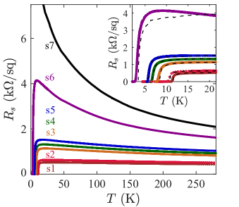
Figure 1 shows temperature dependencies of the sheet resistance for all NbN films under study. for all films gradually rises as temperature decreases and drops to zero at vicinity of . The temperature trend of can be characterized by the resistance ratio parameter , where is the maximal sheet resistance just above the resistive transition. Commonly observed is well-known behavior for disordered NbN films. It reflects sensitivity of electron system to quantum corrections, meanwhile contribution of e-ph scattering is considered to be negligible here. We also observed the suppression of with increasing disorder, which is consistent with the fermionic mechanism of suppression of superconductivity in moderately disordered films (see Appendix B for details).
Table 1 gives an overview of metallic properties for studied NbN films. The details about the carrier density , the Ioffe-Regel (disorder) parameter , the mean free path , the electron diffusivity , and the density of states estimates are provided in Appendix C. High normal-state resistance and low resistance ratio parameter of the magnetron-sputtered NbN films are also known to be strongly influenced by grain-boundary scattering [45, 46, 47], which is related to electron transmission through grain boundaries [48]. One should note that the graininess of ultrathin NbN films is not as pronounced as that of thick films (see AFM studies of ultrathin NbN films in Appendix A). Meanwhile, we assume that the electron transport through the grains can be considered as one of the main factors limiting the mean free path in NbN films (see Appendix C for details).
| (/sq) | (K) | (cm2/s) | (nm) | (T) | (m-3) | (fs) | () | (eV-1m-3) | (/sq) | (ps) | (eV) | ||||
|---|---|---|---|---|---|---|---|---|---|---|---|---|---|---|---|
| s1 | 437 | 0.85 | 6.3 | 11.54 | 0.59 | 3.9 | 14.8 | 1.9 | 0.7 | 3.5 | 4.8 | 497 | 8.3 | 3.05 | 5.9 |
| s2 | 509 | 0.81 | 5.5 | 10.76 | 0.57 | 4.0 | 14.3 | 1.8 | 0.6 | 3.16 | 4.3 | 602 | 7 | 3 | 6.2 |
| s3 | 815 | 0.72 | 3.5 | 8.43 | 0.36 | 3.6 | 17.9 | 1.7 | 0.4 | 2 | 4.3 | 1010 | 20.5 | 3.05 | 5.9 |
| s4 | 912 | 0.69 | 3.2 | 7.02 | 0.35 | 3.8 | 15.3 | 1.6 | 0.35 | 1.9 | 3.9 | 1160 | 21 | 2.4 | 6.1 |
| s5 | 1025 | 0.67 | 2.8 | 6.03 | 0.34 | 4.1 | 13.5 | 1.6 | 0.27 | 1.65 | 3.6 | 1287 | 20 | 2 | 6.6 |
| s6 | 1574 | 0.38 | 2.1 | 3.40 | 0.27 | 4.9 | 9.7 | 1 | 0.28 | 1.5 | 3.0 | 2550 | 30 | 1.7 | 5.0 |
| s7 | 1950 | 0.26 | 1.6 | - | 0.19 | - | - | 1.1 | 0.15 | 1.1 | 2.4 | - | 300 (T=1 K) | 1.7 | 6.9 |
III.2 Magnetoconductance
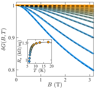
To study inelastic relaxation in NbN films as a function of disorder, we measured magnetoresistance by varying magnetic field in the range from to T at a set of fixed temperatures from to K. The NbN films studied represent quasi two-dimensional (2D) system with respect to characteristic length scales, i.e. the thermal coherence length and the superconducting coherence length (). The dimensionless change in magnetoconductance at the fixed can be determined from the measured using the following expression:
| (1) |
Figure 2 shows typical experimental dependencies of for NbN samples. The data, presented for a representative sample (s5), look similar for other samples.
Applying the fluctuation spectroscopy approach, we fit the experimental data in Figure 2 by the relative magnetoconductance (see the Appendix D for details). In this approach for superconducting samples reflects the change in conductance originated from superconducting fluctuations and the weak localization. Using as a fitting parameter, we estimated the anomalous Maki-Thompson term, which contains information about the temperature-dependent electron phase-breaking rate . Note that the choice of in 2D disordered superconducting films is ambiguous due to disorder induced spatial inhomogeneity of superconducting properties [49, 50, 51]. Nevertheless, in our measurements the choice of barely affects the extracted values of (see Appendix E for details). The best fits of in Figure 2 are shown with black curves with values of varying in under % in respect to the values determined at . It is important to note that the phase-breaking length is larger than the film thickness in a considered temperature range. This fact supports validity of using 2D expressions for NbN films under study. The values of , obtained for the most disordered and non-superconducting sample (s7), are extracted by taking into account only the weak localization term (see Eq. 4b in the Appendix D).
The same approach, with adding the e-e scattering term to the conductivity, can be exploited for fitting of -dependencies above (see the inset of Figure 1). Here we use the expression , where is a fitting parameter and the values of in are those extracted from the magnetoconductance processing. The values of turn out to be close to for moderately-disordered films. The discrepancy between and in the strongly disordered NbN film (s6) may be explained by changing their granular properties (size of granules, intergranular properties) and approaching the Anderson-Mott transition [52].
III.3 Electron phase-breaking rate
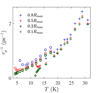
As a next step, we explore the impact of disorder on inelastic scattering in NbN films. Figure 3(a) shows the temperature dependences of for all studied samples. First of all, the data demonstrate the close resemblance of the results for NbN samples with different level of disorder. The data are characterized by close values of , as well as a similar power-law decrease in with lowering temperature. The exact expression for is represented by sum of scattering mechanisms due to superconducting fluctuations , the e-e scattering rate , the spin-flip scattering rate , and the e-ph scattering rate as follows [53]:
| (2a) | |||
| The presence of surface magnetic defects can significantly increase [7, 8] and lead to the -independent behavior at low temperatures [13, 8]. The magnetic disorder in superconductors can lead to a time-reversal symmetry breaking caused by spin-flip scattering, altering superconducting state and suppressing more strongly than the nonmagnetic disorder [54, 55, 56]. Recent studies of Nb and NbN-based devices reveal unintentional surface magnetic disorder due to the unpaired spins in native oxide [57, 58, 59, 60]. Nevertheless, we found that the passivating Si layer on top of NbN films fortunately prevented strong oxidation (see XPS analysis in Appendix A). In addition, the suppression of in our films can be explained by the strong electron interaction (see Appendix B). Thus, we treat the effects of magnetic disorder as negligible in analysis of -dependencies. | |||
The e-e and superconducting fluctuations phase-breaking rates can be defined as [6, 61]:
| (2b) | |||
| (2c) |
where , and . The value of is taken here at the highest temperature of our measurements (300 K), where the effect of e-e interactions is expected to be small [62, 52]. The expression for the e-e scattering rate accounts only for the processes with small energy transfer - the so-called Nyquist quasielastic scattering, which dominates in our experimental temperature range with K. The e-e scattering rate is expected to enhance greatly with increasing disorder [6], but we estimate the increase of as two times for the given change of . Since in our measurements is characterized by a stronger -dependence than the e-e and SC phase-breaking rates, we believe that the e-ph scattering is the dominant dephasing process here. Applying that , where and are fitting constants, we fit the data in Figure 3(a) (see the dashed lines). Table 1 gives an overview of the best-fit values for the power index and , where the latter reflects the e-ph scattering time at .
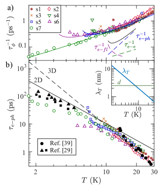
Figure 3(b) shows the temperature dependencies of extracted from the total dephasing rate by subtracting and . We observe that the magnitude and the temperature dependences of for the studied NbN films do not depend on disorder, but demonstrate the non-monotonic temperature dependence: it is proportional to above K, and it modifies to at lower temperatures. To compare our findings with the previous results, we added to Figure 3(b) the experimental data for some different NbN films measured by magnetoconductance in Ref. [39] and extracted from a response to the amplitude-modulated radiation (AMAR method) of NbN detector in Ref. [29, 63]. We observe the close agreement between all experimental data for obtained for various NbN films. Below we will discuss potential mechanisms responsible for the observed rates of the e-ph scattering.
III.4 Electron-phonon scattering in ultrathin films
In search of potential explanation for the observed behavior, we turned to the existing models of the e-ph scattering in thin disordered metals [64, 9, 65]. In general, the e-ph coupling occurs because the passing phonons distort the local lattice structure and conduction electrons respond to the resulting band distortion. A widely used standard model of the low temperature e-ph scattering in bulk metals (i.e. jellium model) [66, 67] assumes (i) a clean three-dimensional (3D) free electron gas with a spherical Fermi surface; (ii) a Debye description of the acoustic phonons; (iii) the scalar deformation potential, expected to be dominant at long-wavelength phonons and (iv) the dimensions of the metal are much longer than the average phonon wavelength (3D phonon spectrum). In this model, the average e-ph scattering rate appropriate for these assumptions is given by [66, 67]: , where is the reduced Planck’s constant, the mass density, the metal volume, the sound speed, the Fermi velocity, and the Fermi energy. In disordered metals the e-ph scattering is non-local with a characteristic size of the interaction region about the phonon wavelength . In the diffusive limit, when , the theory considers the following modifications of the rate [64, 9, 65] and [10], depending on the dominant phonon polarization (longitudinal or transverse ones) and type of disorder (vibrating or static types). One should note that numerous studies of the inelastic scattering with magnetoconductance reveal that there does not exist a universal temperature behavior of in disordered conductors [13]. In particular, the value of the temperature exponent might be quite sensitive to the microscopic quality and the intrinsic material properties such as characteristic of the Fermi surface [68, 69], the dimensionality of the electron and phonon systems [70], nontrivial phonon dispersion [71], etc.
Study of the inelastic scattering with magnetoconductance in NbN films reveal that the power-law index and the magnitude of do not change with increasing disorder in explicit way. Note that the spread of the estimated values of the Fermi energy (see Table 1) is within 10%, so in the further analysis, we assume that the change in the electronic parameters makes a negligible contribution to the change in the e-ph scattering. On the other hand, one would expect that strongly depends on the phonon properties, which, in samples with reduced dimensions, may differ from the Debye spectrum, accepted in the models. Previous studies of the response of thin NbN films to the modulated terahertz radiation revealed a -dependence of the e-ph relaxation rate [29] (see the black-filled symbols in Figure 3(b)), which has been explained by the renormalization of the phonon spectrum in thin films.
In this work, we compare the experimental data in Figure 3(b) with the theoretical predictions for the e-ph scattering in clean case (). One can describe the electron scattering on 3D phonons by the expression [72], and for 2D phonons by . Here is the e-ph coupling constant, and , and are the Debye temperatures and the mean sound velocities, respectively, for 3D and 2D phonons, nm is the NbN lattice constant. The fitting values (the same value as in Ref. [73]), K with m/s for 3D case and , K with m/s for 2D case provide the close agreement with the experimental data in Figure 3(b). Note that the fitting value of is slightly lower the estimated values previously reported for thin NbN films ( K) [15, 39]. Taking into account the average value of , one can estimate the phonon wavelength (here is a constant given in the dominant phonon approximation), which is comparable with the film thickness , see the inset of Figure 3(b). Here the crossover is expected at K. Therefore, the e-ph scattering in ultrathin NbN films can be considered in 3D regime at temperatures higher than , and in 2D regime at low temperatures.
To ensure the condition that the film is two-dimensional for the phonons, one can assume that there is a substantial acoustic mismatch between the film and and the substrate [74, 75]. In that case, the quantization of the phonon spectrum in direction perpendicular to the film may be significant, leading to reduced phonon density of states and, hence, a weakened temperature dependence. Using the fitting parameters K, m/s, and the value of the phonon escape time ps (see Appendix F for details), we estimate the phonon transmission coefficient , which is consistent with the previous results for NbN/Al2O3 interface [39]. This small value of indicates that available directions for the phonon escape from the ultrathin film are strongly restricted.
Another surprising fact is that the observed T-dependences of for NbN films are close to predictions of the simple model for the e-ph scattering in clean metals. Typically, NbN films have a polycrystalline structure [76], which can be considered as a composite of crystalline grains separated by thin amorphous boundaries [77]. In our study, we observe a significant increase of the sheet resistance with change of deposition conditions, which may indicate a change in crystalline properties. At the same time, we see that the disorder weakly affects the e-ph scattering rates in these NbN films. One should note that the disorder in the models of the e-ph scattering in disordered metals [9, 10, 13] is usually treated as point defects, while in NbN films the increase in resistance and decrease in the mean free path may be related to a different origin, for instance, electron tunneling through barriers, which separate NbN grains. Thus, the disorder-independent character of in granular samples might come from the presence of weakly disordered metal grains. However, this assumption requires further theoretical and empirical study.
IV Discussion
In this paper, we investigate the evolution of electronic parameters and inelastic scattering rates with increasing disorder in ultrathin NbN films. We find that the inelastic scattering rates of electrons and their temperature dependencies are close for NbN films of different microscopic quality and with different levels of disorder. Our experimental results in Figure 3 are in agreement with previous studies of the inelastic scattering times in NbN films [29, 39].
One should note that, in detectors, the energy relaxation time due to e-ph scattering differ from by a numerical coefficient , where for , respectively [78]. Thus, the weak dependence on disorder for in NbN films with a higher level of disorder and lower values can facilitate for increase of sensitivity and spectral characteristics of HEBs devices [3] as well as for increase the efficiency of single photon detection of SNSPDs. In the latter case, the fast inelastic scattering and the electron diffusivity both affect the hotspot size and the superconducting gap suppression [79]. This expectation correlates with a recent breakthrough in detection efficiency in SNSPDs, when one uses NbN films with high normal-state resistance values [80, 17, 81]. On the other hand, one should keep in mind that the operation of the detectors is also limited by the phonon escape rate, which is proportional to the sound velocity. As shown in Section D, the analysis of -dependence indicates low values of the sound velocity, which in turn can affect the phonon escape rate and limit the device response. Thus, further experimental study of the features of phonon transport in ultrathin disordered metals is advisable.
In summary, we observe the disorder-independent character of the electron-phonon scattering time in ultrathin NbN films. The observed results are not described by existing models of the e-ph scattering in disordered metals. The experimental values of , measured above K, are proportional to , expected for the electron scattering on three-dimensional acoustic phonons in clean case. At lower temperatures, modifies to , which is likely due to lowering the dimensionality of the phonons involved in the e-ph scattering. Our results call for further theoretical and experimental studies of the e-ph scattering in the presence of strong disorder.
Acknowledgement
We acknowledge valuable discussions with V.S. Khrapai and M. Sidorova. We are grateful to S.V. Simonov for their assistance with the X-ray studies. X-ray studies were performed using Rigaku SmartLab SE diffractometer at shared facility center of ISSP RAS. The growth of NbN films, material characterization and magnetotransport measurements were funded by the RFBR project No. 19-32-60076. The surface analysis and analysis of transport properties were carried out with the financial support of the Ministry of science and higher education of the Russian Federation in the framework of the Agreement No. 075-11-2022-026 dated 06.04.2022.
Appendix A: X-ray diffraction, XPS analysis and atomic force microscopy of a NbN film
Structural characterization of a 2.5-nm thick NbN sample (s1) is shown in Figure 4. We plot the X-ray diffraction (XRD) data for a coupled scan and identify main diffraction peaks of NbN (101), (202) and Al2O3 (012), (024) for film and for substrate, respectively. The x-ray data indicates that NbNx has a tetragonal phase (-phase), which is generally characterized by [82]. This phase is considered to be a deformed cubic phase (-phase) with a similar transition temperature and the electronic spectrum as in a -phase but has less N content [83, 84]. The observed -phase is in accordance with the phase diagram of NbN calculated as a function of the substrate heating temperature [85].
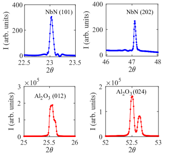
Figure 5 displays the experimental data on X-ray photoelectron spectroscopy (XPS) presented for the least-disordered sample in the set (s1). The XPS studies of samples surfaces were performed with the help of the electron-ion spectroscopy module based on Nanofab 25 (NT-MDT) platform in the analysis chamber an ultrahigh oil-free vacuum about Pa. Figure 5 shows decomposition of XPS lines of an element of interest (Nb, N, O, Al) into component peaks that reveals presence of different phases in the sample (NbNx, NbN-Si).The XPS result are obtained on the base of the method described in Ref. [86]. The results allow to extract thicknesses of layers of different phases. The data for the studied NbN sample is presented in Table 2.
| Formula | (nm) | |
|---|---|---|
| 1 | SiO2 | 1.030.19 |
| 2 | Si | 5.30.5 |
| 3 | NbN-Si | 0.590.11 |
| 4 | NbN | not records |
| Substrate | Al2O3 | Inf |
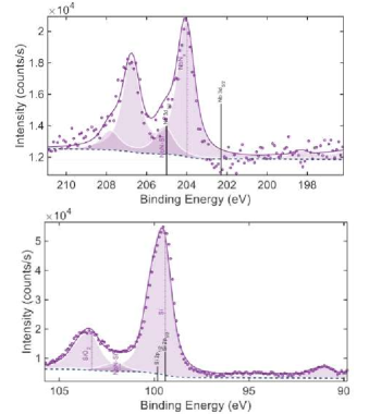
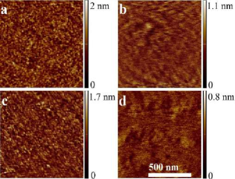
Figure 6 shows the atomic force microscope (AFM) images of a few NbN samples covered by 5-nm thick Si layer and a sapphire substrate. The AFM images are obtained with NT-MDT (INTEGRA series) setup in classical contact mode. The rms surface roughness of NbN films is below 0.2 nm, which corresponds to atomically smooth surface. In contrast to thick NbN films ( nm), which have a pronounced granular structure [87], ultrathin NbN can be considered as a quasiamorphous matrix with the grain size smaller the film thickness.
Surface topography of NbNx is known to be strongly affected by the substrate heating temperature and the nitrogen partial pressure during deposition process [88]. As shown in Figure 6, the microstructure of the samples deposited at high (s1, s6) is compact-grained, since heating of the substrate increases mobility of adatoms and increases density of the film. The sample deposited at room temperature (s5) is characterized by less compact microstructure without pronounced grains. As the nitrogen content in the system changed, various and interrelated types of crystallographic structures are expected to form [85, 88]. With increase of the nitrogen background pressure, one can expect that the kinetic energy and flux of the ablated materials are reduced, and the latter results in less nitrogen ratio in NbNx film as well as a decrease in material density [82].
Appendix B: variation of in ultrathin NbN films
Here we discuss the correlation between and , shown in Figure 7. The breakdown of the superconductivity with the increase of disorder can be related to two different, but not mutually exclusive effects [1]. The first effect results from a decrease of electronic screening, which enhances the e-e repulsion and partially cancels the e-ph mediated attractive interaction. This fermionic effect leads to a mechanism described in Ref. [89, 90]. The second effect comes from the disorder-induced decrease in superfluid density, which makes a superconductor susceptible to phase fluctuations [91, 92]. The latter is known as a bosonic mechanism.
As shown in Figure 7, the suppression of follows the expectations of the fermionic mechanism, which can be expressed in the following form [90]:
| (3) |
where the first term in rhs corresponds to the three-dimensional ballistic motion of electrons, the second term in rhs is related to 2D diffusive motion of electrons. Here is the critical temperature in bulk, is the electron–electron coupling constant, and is the material dependent coefficient of the order of unity. The experimental data is in good agreement with Eq. 3 taking , m-1, =40 fs and treating K and as the fitting parameters, see the red solid line in Figure 7. It is instructive to note that suppression of , related to 2D diffusive nature of electron motion, is weak here (the black dashed line), and it is likely determined by the 3D ballistics [90]. The observed dependence can be associated with the following hierarchy of length scales in the studied NbN films, and thus the suppression of is likely to be controlled by parameter rather than . One should also note that the change in the density of states at the Fermi level is small (see values of in Table 1) and cannot distort the analysis within the framework of the fermionic scenario.
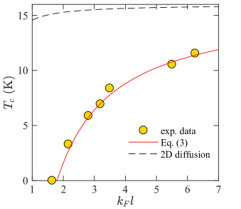
Meanwhile, in the previous studies [30, 16], the electronic system in NbN films was observed to undergo the fermionic scenario at moderate level of disorder () and cross to a bosonic route at stronger disorder (). The estimated level of disorder in our NbN films, in comparison to those in Ref. [16], shows that the e-e repulsion can play a major role in destruction of the superconducting state for samples s1-s5, whereas the strong phase fluctuations due to small superfluid density can be more pronounced for the most disordered samples in this study (s6 and s7). The latter means that these two effects, which provide the disorder-induced suppression of , should be considered collectively. However, we leave further refinements beyond the scope of this work, since the exact microscopic picture of the suppression of does not play a large role in the results obtained for (see Appendix E for details).
Appendix C: electron transport
We calculate all electronic parameters at the highest temperature of our measurements (300 K), where the effect of e-e interactions is expected to be small [62]. Firstly, to estimate the Hall coefficient we consider the expression [6], where is an empirical parameter [93]. Using the value of we derive the carrier density , where is the electron charge. It is also important to note that samples s1-s5 are characterized by a moderate change ( %) in the carrier density at increase of in two times. Meanwhile, the most disordered samples (s6 and s7) are characterized by a twofold decrease of at three- and fourfold increase of . The latter change in can be a result of the increase of Nb and N vacancies due to the increase of the nitrogen partial pressure in the mixture during deposition of NbN [15].
To characterize electron transport, we estimate the mean free path , the elastic scattering time and the single-spin density of states (DOS) at the Fermi level assuming the free electron model [94] and using the following expressions , , and , where is the Fermi wavevector. We believe that this ab-initio estimates are well justified, since , which is in order of the lattice constant in our disordered NbN films, thereby a possible Fermi surface anisotropy can be negligible. The electronic transport is also characterized by the Ioffe-Regel parameter , which is a common indicator of the disorder in homogeneously disordered material. All estimated parameters are listed in Table 1. In addition, Figure 8(a) shows the relationship between the experimental values of and , which can be approximated as , where m/s is the Fermi velocity determined as a fitting parameter here. The estimate of is two times lower than the one previously reported [32], and it corresponds to the effective mass of charge carriers , which decreases from to as increases (here is the mass of a free electron). Note that taking into account these values of allows to correct underestimation of determined from optical measurements in NbN [95].
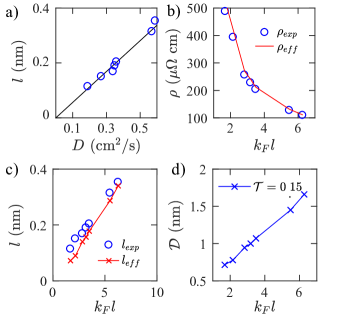
In an attempt to understand electron transport in NbN films better, we performed a simple analysis of resistivity in terms of the grain boundary model [48, 45, 46, 47]. In general, resistivity of granular films can be qualitatively given in the following way [48]: , where is the mean free path in absence of granularity, is the mean grain size, is the transmission probability of electrons through the grain boundary, is the carrier density of bulk material without crystal boundaries. Resistance here is increased since the effective mean free path is reduced due to the reflection on the grain boundaries: . Figure 8(b-d) demonstrates an attempt to evaluate the effect of granularity on resistivity of the studied NbN films. In Figure 8(b-c) we compare the values of resistivity and the mean free path deduced from transport measurements with and as a function of disorder (). Taking into account cm-3 and nm reported for crystalline NbN films [96], we evaluated , which is a function of the coupled parameters and . In contrast to thick NbN films, which exhibit a pronounced polycrystalline structure [97], ultrathin NbN films can represent a quasiamorphous matrix with the expected grain size smaller than the film thickness but larger than the characteristic unit cell. Taking into account the fixed value [47], we estimate the effective size of a crystalline grain in studied NbN samples ( Figure 8(d)), which falls within the range , where nm is the film thickness and nm is the lattice constant [98, 73]. As revealed in AFM studies (see Appendix A), ultrathin NbN films grown at different substrate temperatures are characterized by different grain packing density: NbN films deposited at high typically have a more compact and dense microstructure than films deposited at low . In case of films deposited at different nitrogen partial pressures, this difference is not so obvious. Meanwhile, one can expect a decrease in the effective grain size for NbN films deposited at lower , as well as under excessive nitrogen partial pressure [82]. Thus, increase of disorder in NbN films may reflect change of microstructure due to emergence of some granular structure as well as an increase in the number of point scatterers, such as vacancies at lattice sites.
Appendix D: Magnetoconductance
To derive from the magnetoconductance at temperatures , we fit data with the dimensionless change in magnetoconductance, which is given by expression:
| (4a) | |||
| where and are a sum of four terms of quantum corrections to conductivity at finite and zero magnetic fields: the weak localization (WL), the Aslamazov-Larkin (AL) term, the density of states (DOS) contribution term, and Maki-Thomson (MT) term.
The sum of these terms is given by the following expression [53, 99, 100, 101]: | |||
| (4b) | |||
| where is Digamma function, and , , , , and . The characteristic fields are defined as , , and , where , , and are the relaxation time for elastic, spin-orbit, and phase-breaking scattering, respectively. The spin-orbit time can be roughly estimated using ps, where is the elastic scattering time, is the fine structure constant, and is the effective atomic number of material (). The magnetic scattering is assumed to negligible () since the samples are covered with a protective layer. The coefficient in MT term is given as [100]: | |||
| (4c) | |||
| where and .
Note, that AL and DOS terms in the Eq.(4b) are asymptotics for low temperatures . Nevertheless, the derivation of at high temperatures do not dependent on presence of AL and DOS terms in the Eq.(4b).
In the limit of zero magnetic field, Eq.(4b) with adding the e-e contribution [6] can be transformed to: | |||
| (4d) | |||
The Eq.(4d) can be used for fitting -curve at low temperatures . To fit high- part of resistance we replace the AL and DOS terms with and asymptotics, respectively [99].
Appendix E: Influence of the choice of on estimates of
To fit the experimental data for the magnetoconductance with the fluctuation spectroscopy, we use as a fitting parameter. Nominally, the critical temperature in our study is determined as the temperature at which . Figure 9 shows that the choice of at different setpoints barely affects the extracted phase-breaking time .
. The data are presented for two samples: s1 (cross-shaped symbols) and s6 (round symbols).
Appendix F: Estimate of the phonon escape time
The characteristic phonon escape time can be found as [102], where is the phonon heat capacity in the 3D Debye model and is the heat flow rate limited by the Kapitza resistance. Taking into account the experimentally determined cooling rate for NbN-Al2O3 interface WK-4m-2 [102], nm, nm, and K, we obtain ps.
References
- Sacépé et al. [2020] B. Sacépé, M. Feigel’man, and T. M. Klapwijk, Quantum breakdown of superconductivity in low-dimensional materials, Nat. Phys. 16, 734 (2020).
- Semenov [2021] A. D. Semenov, Superconducting nanostrip single-photon detectors some fundamental aspects in detection mechanism, technology and performance, Supercond. Sci. Technol. 34, 054002 (2021).
- Shurakov et al. [2015] A. Shurakov, Y. Lobanov, and G. Goltsman, Superconducting hot-electron bolometer: from the discovery of hot-electron phenomena to practical applications, Supercond. Sci. Technol. 29, 023001 (2015).
- Zmuidzinas [2012] J. Zmuidzinas, Superconducting microresonators: Physics and applications, Annu. Rev. Condens. Matter Phys. 3, 169 (2012).
- de Visser et al. [2021] P. J. de Visser, S. A. de Rooij, V. Murugesan, D. J. Thoen, and J. J. Baselmans, Phonon-trapping-enhanced energy resolution in superconducting single-photon detectors, Phys. Rev. Applied 16, 034051 (2021).
- Altshuler and Aronov [1985] B. Altshuler and A. Aronov, in Electron–Electron Interactions in Disordered Systems (Elsevier Science Publishers B.V.,Amsterdam, 1985) pp. 1–153.
- Anthore et al. [2003] A. Anthore, F. Pierre, H. Pothier, and D. Esteve, Magnetic-Field-Dependent Quasiparticle Energy Relaxation in Mesoscopic Wires, Phys. Rev. Lett. 90, 076806 (2003).
- Huard et al. [2005] B. Huard, A. Anthore, N. O. Birge, H. Pothier, and D. Esteve, Effect of magnetic impurities on energy exchange between electrons, Phys. Rev. Lett. 95, 036802 (2005).
- Schmid [1973] A. Schmid, Electron-phonon interaction in an impure metal, Z. Physik 259, 421 (1973).
- Sergeev and Mitin [2000] A. Sergeev and V. Mitin, Electron-phonon interaction in disordered conductors: Static and vibrating scattering potentials, Phys. Rev. B 61, 6041 (2000).
- Shtyk and Feigel’man [2015] A. Shtyk and M. Feigel’man, Ultrasonic attenuation via energy diffusion channel in disordered conductors, Phys. Rev. B 92, 195101 (2015).
- Gershenson et al. [2001] M. E. Gershenson, D. Gong, T. Sato, B. S. Karasik, and A. V. Sergeev, Millisecond electron–phonon relaxation in ultrathin disordered metal films at millikelvin temperatures, Appl. Phys. Lett. 79, 2049 (2001).
- Lin and Bird [2002] J. J. Lin and J. P. Bird, Recent experimental studies of electron dephasing in metal and semiconductor mesoscopic structures, J. Phys.: Condens. Matter 14, R501 (2002).
- Karvonen et al. [2005] J. T. Karvonen, L. J. Taskinen, and I. J. Maasilta, Observation of disorder-induced weakening of electron-phonon interaction in thin noble-metal films, Phys. Rev. B 72, 012302 (2005).
- Chockalingam et al. [2008] S. P. Chockalingam, M. Chand, J. Jesudasan, V. Tripathi, and P. Raychaudhuri, Superconducting properties and Hall effect of epitaxial NbN thin films, Phys. Rev. B 77, 214503 (2008).
- Chand et al. [2012] M. Chand, G. Saraswat, A. Kamlapure, M. Mondal, S. Kumar, J. Jesudasan, V. Bagwe, L. Benfatto, V. Tripathi, and P. Raychaudhuri, Phase diagram of the strongly disordered -wave superconductor NbN close to the metal-insulator transition, Phys. Rev. B 85, 014508 (2012).
- Zolotov et al. [2021] P. I. Zolotov, A. V. Semenov, A. V. Divochiy, G. N. Goltsman, N. R. Romanov, and T. M. Klapwijk, Dependence of Photon Detection efficiency on Normal-State Sheet Resistance in Marginally Superconducting Films of NbN, IEEE Trans. Appl. Supercond. 31, 1 (2021).
- Gol’tsman et al. [2001] G. N. Gol’tsman, O. Okunev, G. Chulkova, A. Lipatov, A. Semenov, K. Smirnov, B. Voronov, A. Dzardanov, C. Williams, and R. Sobolewski, Picosecond superconducting single-photon optical detector, Appl. Phys. Lett. 79, 705 (2001).
- Divochiy et al. [2018] A. Divochiy, M. Misiaszek, Y. Vakhtomin, P. Morozov, K. Smirnov, P. Zolotov, and P. Kolenderski, Single photon detection system for visible and infrared spectrum range, Opt. Lett. 43, 6085 (2018).
- Tretyakov et al. [2011] I. Tretyakov, S. Ryabchun, M. Finkel, A. Maslennikova, N. Kaurova, A. Lobastova, B. Voronov, and G. Gol’tsman, Low noise and wide bandwidth of NbN hot-electron bolometer mixers, Appl. Phys. Lett. 98, 033507 (2011).
- Annunziata et al. [2010] A. J. Annunziata, D. F. Santavicca, L. Frunzio, G. Catelani, M. J. Rooks, A. Frydman, and D. E. Prober, Tunable superconducting nanoinductors, Nanotechnology 21, 445202 (2010).
- Niepce et al. [2019] D. Niepce, J. Burnett, and J. Bylander, High kinetic inductance nanowire superinductors, Phys. Rev. Applied 11, 044014 (2019).
- Peltonen et al. [2013] J. T. Peltonen, O. V. Astafiev, Y. P. Korneeva, B. M. Voronov, A. A. Korneev, I. M. Charaev, A. V. Semenov, G. N. Golt’sman, L. B. Ioffe, T. M. Klapwijk, and J. S. Tsai, Coherent flux tunneling through NbN nanowires, Phys. Rev. B 88, 220506 (2013).
- Arutyunov et al. [2016] K. Y. Arutyunov, A. Ramos-Álvarez, A. V. Semenov, Y. P. Korneeva, P. P. An, A. A. Korneev, A. Murphy, A. Bezryadin, and G. N. Gol’tsman, Superconductivity in highly disordered NbN nanowires, Nanotechnology 27, 47LT02 (2016).
- Peltonen et al. [2016] J. T. Peltonen, Z. H. Peng, Y. P. Korneeva, B. M. Voronov, A. A. Korneev, A. V. Semenov, G. N. Gol’tsman, J. S. Tsai, and O. V. Astafiev, Coherent dynamics and decoherence in a superconducting weak link, Phys. Rev. B 94, 180508 (2016).
- Constantino et al. [2018] N. G. N. Constantino, M. S. Anwar, O. W. Kennedy, M. Dang, P. A. Warburton, and J. C. Fenton, Emergence of Quantum Phase-Slip Behaviour in Superconducting NbN Nanowires: DC Electrical Transport and Fabrication Technologies, Nanomaterials 8, 442 (2018).
- de Graaf et al. [2018] S. E. de Graaf, S. T. Skacel, T. Hönigl-Decrinis, R. Shaikhaidarov, H. Rotzinger, S. Linzen, M. Ziegler, U. Hübner, H.-G. Meyer, V. Antonov, E. Il’ichev, A. V. Ustinov, A. Y. Tzalenchuk, and O. V. Astafiev, Charge quantum interference device, Nat. Phys. 14, 590 (2018).
- Shaikhaidarov et al. [2022] R. S. Shaikhaidarov, K. H. Kim, J. W. Dunstan, I. V. Antonov, S. Linzen, M. Ziegler, D. S. Golubev, V. N. Antonov, E. V. Il’ichev, and O. V. Astafiev, Quantized current steps due to the a.c. coherent quantum phase-slip effect, Nature 608, 45 (2022).
- Gousev et al. [1994] Y. P. Gousev, G. N. Gol’tsman, A. D. Semenov, E. M. Gershenzon, R. S. Nebosis, M. A. Heusinger, and K. F. Renk, Broadband ultrafast superconducting NbN detector for electromagnetic radiation, J. Appl. Phys. 75, 3695 (1994).
- Mondal et al. [2011a] M. Mondal, S. Kumar, M. Chand, A. Kamlapure, G. Saraswat, G. Seibold, L. Benfatto, and P. Raychaudhuri, Role of the Vortex-Core Energy on the Berezinskii-Kosterlitz-Thouless Transition in Thin Films of NbN, Phys. Rev. Lett. 107, 217003 (2011a).
- Delacour et al. [2012] C. Delacour, B. Pannetier, J.-C. Villegier, and V. Bouchiat, Quantum and Thermal Phase Slips in Superconducting Niobium Nitride (NbN) Ultrathin Crystalline Nanowire: Application to Single Photon Detection, Nano Lett. 12, 3501 (2012).
- Mondal et al. [2013] M. Mondal, A. Kamlapure, S. C. Ganguli, J. Jesudasan, V. Bagwe, L. Benfatto, and P. Raychaudhuri, Enhancement of the finite-frequency superfluid response in the pseudogap regime of strongly disordered superconducting films, Sci. Rep. 3, 1357 (2013).
- Noat et al. [2013] Y. Noat, V. Cherkez, C. Brun, T. Cren, C. Carbillet, F. Debontridder, K. Ilin, M. Siegel, A. Semenov, H.-W. Hübers, and D. Roditchev, Unconventional superconductivity in ultrathin superconducting NbN films studied by scanning tunneling spectroscopy, Phys. Rev. B 88, 014503 (2013).
- Carbillet et al. [2020] C. Carbillet, V. Cherkez, M. A. Skvortsov, M. V. Feigel’man, F. Debontridder, L. B. Ioffe, V. S. Stolyarov, K. Ilin, M. Siegel, D. Roditchev, T. Cren, and C. Brun, Spectroscopic evidence for strong correlations between local superconducting gap and local Altshuler-Aronov density of states suppression in ultrathin NbN films, Phys. Rev. B 102, 024504 (2020).
- Il’in et al. [2000] K. S. Il’in, M. Lindgren, M. Currie, A. D. Semenov, G. N. Gol’tsman, R. Sobolewski, S. I. Cherednichenko, and E. M. Gershenzon, Picosecond hot-electron energy relaxation in NbN superconducting photodetectors, Appl. Phys. Lett. 76, 2752 (2000).
- Zhang et al. [2003] J. Zhang, W. Słysz, A. Pearlman, A. Verevkin, R. Sobolewski, O. Okunev, G. Chulkova, and G. N. Gol’tsman, Time delay of resistive-state formation in superconducting stripes excited by single optical photons, Phys. Rev. B 67, 132508 (2003).
- Lin et al. [2013a] S.-Z. Lin, O. Ayala-Valenzuela, R. D. McDonald, L. N. Bulaevskii, T. G. Holesinger, F. Ronning, N. R. Weisse-Bernstein, T. L. Williamson, A. H. Mueller, M. A. Hoffbauer, M. W. Rabin, and M. J. Graf, Characterization of the thin-film NbN superconductor for single-photon detection by transport measurements, Phys. Rev. B 87, 184507 (2013a).
- Zhang et al. [2018] L. Zhang, L. You, X. Yang, J. Wu, C. Lv, Q. Guo, W. Zhang, H. Li, W. Peng, Z. Wang, and X. Xie, Hotspot relaxation time of NbN superconducting nanowire single-photon detectors on various substrates, Sci. Rep. 8, 1486 (2018).
- Sidorova et al. [2020] M. Sidorova, A. Semenov, H.-W. Hübers, K. Ilin, M. Siegel, I. Charaev, M. Moshkova, N. Kaurova, G. N. Goltsman, X. Zhang, and A. Schilling, Electron energy relaxation in disordered superconducting NbN films, Phys. Rev. B 102, 054501 (2020).
- Zhang et al. [2020] L. Zhang, L. You, W. Peng, and Z. Wang, Quasiparticle scattering time in NbN superconducting thin films, Phys. C: Supercond. Appl. 579, 1353773 (2020).
- Linzen et al. [2017] S. Linzen, M. Ziegler, O. V. Astafiev, M. Schmelz, U. Hübner, M. Diegel, E. Il’ichev, and H.-G. Meyer, Structural and electrical properties of ultrathin niobium nitride films grown by atomic layer deposition, Supercond. Sci. Technol. 30, 035010 (2017).
- Knehr et al. [2021] E. Knehr, M. Ziegler, S. Linzen, K. Ilin, P. Schanz, J. Plentz, M. Diegel, H. Schmidt, E. Il’ichev, and M. Siegel, Wafer-level uniformity of atomic-layer-deposited niobium nitride thin films for quantum devices, J. Vac. Sci. Technol. A: Vac. Surf. 39, 052401 (2021).
- Shinozaki et al. [2019] B. Shinozaki, S. Ezaki, T. Odou, T. Asano, and K. Makise, Anomalous electron inelastic scattering rate probed via superconducting fluctuation in epitaxial NbN thin films, Phys. C: Supercond. Appl. 567, 1353547 (2019).
- Sidorova et al. [2021] M. Sidorova, A. D. Semenov, H.-W. Hübers, S. Gyger, S. Steinhauer, X. Zhang, and A. Schilling, Magnetoconductance and photoresponse properties of disordered nbtin films, Phys. Rev. B 104, 184514 (2021).
- Nigro et al. [1988] A. Nigro, G. Nobile, M. G. Rubino, and R. Vaglio, Electrical resistivity of polycrystalline niobium nitride films, Phys. Rev. B 37, 3970 (1988).
- Tyan and Lue [1994] J. Tyan and J. T. Lue, Grain boundary scattering in the normal state resistivity of superconducting NbN thin films, J. Appl. Phys. 75, 325 (1994).
- Senapati et al. [2006] K. Senapati, N. K. Pandey, R. Nagar, and R. C. Budhani, Normal-state transport and vortex dynamics in thin films of two structural polymorphs of superconducting nbn, Phys. Rev. B 74, 104514 (2006).
- Reiss et al. [1986] G. Reiss, J. Vancea, and H. Hoffmann, Grain-boundary resistance in polycrystalline metals, Phys. Rev. Lett. 56, 2100 (1986).
- Benfatto et al. [2009] L. Benfatto, C. Castellani, and T. Giamarchi, Broadening of the Berezinskii-Kosterlitz-Thouless superconducting transition by inhomogeneity and finite-size effects, Phys. Rev. B 80, 214506 (2009).
- Caprara et al. [2011] S. Caprara, M. Grilli, L. Benfatto, and C. Castellani, Effective medium theory for superconducting layers: A systematic analysis including space correlation effects, Phys. Rev. B 84, 014514 (2011).
- Baturina et al. [2012] T. I. Baturina, S. V. Postolova, A. Y. Mironov, A. Glatz, M. R. Baklanov, and V. M. Vinokur, Superconducting phase transitions in ultrathin TiN films, Europhys. Lett. 97, 17012 (2012).
- Mondal et al. [2011b] M. Mondal, M. Chand, A. Kamlapure, J. Jesudasan, V. C. Bagwe, S. Kumar, G. Saraswat, V. Tripathi, and P. Raychaudhuri, Phase Diagram and Upper Critical Field of Homogeneously Disordered Epitaxial 3-Dimensional NbN Films, J. Supercond. Nov. Magn. 24, 341 (2011b).
- Varlamov et al. [2018] A. A. Varlamov, A. Galda, and A. Glatz, Fluctuation spectroscopy: From Rayleigh-Jeans waves to Abrikosov vortex clusters, Rev. Mod. Phys. 90, 015009 (2018).
- Abrikosov and Gor’kov [1961] A. Abrikosov and L. Gor’kov, Contribution to the theory of superconducting alloys with paramagnetic impurities, Sov. Phys. JETP 12, 1243 (1961).
- Müller-Hartmann and Zittartz [1971] E. Müller-Hartmann and J. Zittartz, Kondo effect in superconductors, Phys. Rev. Lett. 26, 428 (1971).
- Fominov et al. [2011] Y. V. Fominov, M. Houzet, and L. I. Glazman, Surface impedance of superconductors with weak magnetic impurities, Phys. Rev. B 84, 224517 (2011).
- Rogachev et al. [2005] A. Rogachev, A. T. Bollinger, and A. Bezryadin, Influence of High Magnetic Fields on the Superconducting Transition of One-Dimensional Nb and MoGe Nanowires, Phys. Rev. Lett. 94, 017004 (2005).
- Kumar et al. [2016] P. Kumar, S. Sendelbach, M. A. Beck, J. W. Freeland, Z. Wang, H. Wang, C. C. Yu, R. Q. Wu, D. P. Pappas, and R. McDermott, Origin and reduction of magnetic flux noise in superconducting devices, Phys. Rev. Applied 6, 041001 (2016).
- Samsonova et al. [2021] A. S. Samsonova, P. I. Zolotov, E. M. Baeva, A. I. Lomakin, N. A. Titova, A. I. Kardakova, and G. N. Goltsman, Signatures of surface magnetic disorder in niobium films, IEEE Trans. Appl. Supercond. 31, 1 (2021).
- Sheridan et al. [2021] E. Sheridan, T. F. Harrelson, E. Sivonxay, K. A. Persson, M. V. P. Altoé, I. Siddiqi, D. F. Ogletree, D. I. Santiago, and S. M. Griffin, Microscopic Theory of Magnetic Disorder-Induced Decoherence in Superconducting Nb Films (2021), arXiv:2111.11684 .
- Brenig et al. [1985] W. Brenig, M.-c. Chang, E. Abrahams, and P. Wölfle, Inelastic scattering time above the superconductivity transition in two dimensions: Dependence on disorder and magnetic field, Phys. Rev. B 31, 7001 (1985).
- Khodas and Finkel’stein [2003] M. Khodas and A. M. Finkel’stein, Hall coefficient in an interacting electron gas, Phys. Rev. B 68, 155114 (2003).
- [63] The dephasing time due to e-ph scattering is identical to the single-particle e-ph scattering time, .The e-ph energy relaxation time, measured by the AMAR method, is proportional to the with a proportionality coefficient, which depends on the exponent : it is about 0.6 for .
- Pippard [1955] A. Pippard, CXXII. Ultrasonic attenuation in metals, Philos. Mag. 46, 1104 (1955).
- Rammer and Schmid [1986] J. Rammer and A. Schmid, Destruction of phase coherence by electron-phonon interactions in disordered conductors, Phys. Rev. B 34, 1352 (1986).
- Gantmakher [1974] V. F. Gantmakher, The experimental study of electron-phonon scattering in metals, Rep. Prog. Phys. 37, 317 (1974).
- Wellstood et al. [1994] F. C. Wellstood, C. Urbina, and J. Clarke, Hot-electron effects in metals, Phys. Rev. B 49, 5942 (1994).
- Prunnila et al. [2005] M. Prunnila, P. Kivinen, A. Savin, P. Törmä, and J. Ahopelto, Intervalley-scattering-induced electron-phonon energy relaxation in many-valley semiconductors at low temperatures, Phys. Rev. Lett. 95, 206602 (2005).
- Qu et al. [2005] S.-X. Qu, A. N. Cleland, and M. R. Geller, Hot electrons in low-dimensional phonon systems, Phys. Rev. B 72, 224301 (2005).
- Sergeev et al. [2005] A. Sergeev, M. Y. Reizer, and V. Mitin, Deformation electron-phonon coupling in disordered semiconductors and nanostructures, Phys. Rev. Lett. 94, 136602 (2005).
- Ono [2020] S. Ono, Low-temperature electron-phonon relaxation in Cu and Ag thin films, Phys. Rev. B 101, 201404 (2020).
- Pethick and Smith [1979] C. Pethick and H. Smith, Relaxation and collective motion in superconductors: a two-fluid description, Ann. Phys. 119, 133 (1979).
- Babu and Guo [2019] K. R. Babu and G.-Y. Guo, Electron-phonon coupling, superconductivity, and nontrivial band topology in NbN polytypes, Phys. Rev. B 99, 104508 (2019).
- Kaplan [1979] S. B. Kaplan, Acoustic matching of superconducting films to substrates, J. Low Temp. Phys. 37, 343 (1979).
- Sidorova et al. [2018] M. V. Sidorova, A. G. Kozorezov, A. V. Semenov, Y. P. Korneeva, M. Y. Mikhailov, A. Y. Devizenko, A. A. Korneev, G. M. Chulkova, and G. N. Goltsman, Nonbolometric bottleneck in electron-phonon relaxation in ultrathin WSi films, Phys. Rev. B 97, 184512 (2018).
- Lin et al. [2013b] S.-Z. Lin, O. Ayala-Valenzuela, R. D. McDonald, L. N. Bulaevskii, T. G. Holesinger, F. Ronning, N. R. Weisse-Bernstein, T. L. Williamson, A. H. Mueller, M. A. Hoffbauer, M. W. Rabin, and M. J. Graf, Characterization of the thin-film NbN superconductor for single-photon detection by transport measurements, Phys. Rev. B 87, 184507 (2013b).
- Zhang et al. [2009] H. Zhang, D. J. Srolovitz, J. F. Douglas, and J. A. Warren, Grain boundaries exhibit the dynamics of glass-forming liquids, Proc. Natl. Acad. Sci. 106, 7735 (2009).
- Il’in et al. [1998] K. S. Il’in, N. G. Ptitsina, A. V. Sergeev, G. N. Gol’tsman, E. M. Gershenzon, B. S. Karasik, E. V. Pechen, and S. I. Krasnosvobodtsev, Interrelation of resistivity and inelastic electron-phonon scattering rate in impure NbC films, Phys. Rev. B 57, 15623 (1998).
- Vodolazov [2017] D. Y. Vodolazov, Single-photon detection by a dirty current-carrying superconducting strip based on the kinetic-equation approach, Phys. Rev. Applied 7, 034014 (2017).
- Hofherr et al. [2010] M. Hofherr, D. Rall, K. Ilin, M. Siegel, A. Semenov, H.-W. Hübers, and N. A. Gippius, Intrinsic detection efficiency of superconducting nanowire single-photon detectors with different thicknesses, J. Appl. Phys. 108, 014507 (2010).
- Korneeva et al. [2021] Y. P. Korneeva, N. N. Manova, M. A. Dryazgov, N. O. Simonov, P. I. Zolotov, and A. A. Korneev, Influence of sheet resistance and strip width on the detection efficiency saturation in micron-wide superconducting strips and large-area meanders, Supercond. Sci. Technol. 34, 084001 (2021).
- Farha [2013] A. H. Farha, Investigation of NbNx Thin Films and Nanoparticles Grown by Pulsed Laser Deposition and Thermal Diffusion, Ph.D. thesis, Old Dominion University, Norfolk (2013).
- Ethridge et al. [1996] E. C. Ethridge, S. C. Erwin, and W. E. Pickett, Nb4N3: Polymorphism in crystalline niobium nitrides, Phys. Rev. B 53, 12563 (1996).
- Pan et al. [2021] Y. Pan, H. Zhou, L. Zhang, H. Li, Y. Tang, H. Yu, M. Si, L. You, and Z. Wang, Superconducting nanowire single-photon detector made of ultrathin -Nb4N3 film for mid-infrared wavelengths, Supercond. Sci. Technol. 34, 074001 (2021).
- Scheerer [1979] B. Scheerer, Preparation of NbN single crystals (Karlsruhe: Kernforschungszentrum Karlsruhe, 1979).
- Lubenchenko et al. [2018] A. V. Lubenchenko, A. A. Batrakov, A. B. Pavolotsky, O. I. Lubenchenko, and D. A. Ivanov, XPS study of multilayer multicomponent films, Appl. Surf. Sci. 427, 711 (2018).
- Soldatenkova et al. [2021a] M. D. Soldatenkova, A. D. Triznova, E. M. Baeva, P. I. Zolotov, A. I. Lomakin, A. I. Kardakova, and G. N. Goltsman, Normal-state transport in superconducting NbN films on r-cut sapphire, J. Phys.: Conf. Ser. 2086, 012212 (2021a).
- Benkahoul [2005] M. Benkahoul, Niobium nitride based thin films deposited by dc reactive magnetron sputtering: NbN, NbSiN and NbAlN, Ph.D. thesis, Université de Constantine, Lausanne (2005).
- Finkel’stein [1994] A. Finkel’stein, Suppression of superconductivity in homogeneously disordered systems, Phys. B: Condens. Matter 197, 636 (1994).
- Antonenko and Skvortsov [2020] D. S. Antonenko and M. Skvortsov, Suppression of Superconductivity in Disordered Films: Interplay of Two-Dimensional Diffusion and Three-Dimensional Ballistics, JEPT Letters 112, 428 (2020).
- Raychaudhuri and Dutta [2021] P. Raychaudhuri and S. Dutta, Phase fluctuations in conventional superconductors, J. Phys.: Condens. Matter 34, 083001 (2021).
- Dutta et al. [2022] S. Dutta, P. Raychaudhuri, S. S. Mandal, and T. V. Ramakrishnan, Superfluid density in conventional superconductors: from clean to strongly disordered, J. Phys.: Condens. Matter 34, 335601 (2022).
- Chand et al. [2009] M. Chand, A. Mishra, Y. M. Xiong, A. Kamlapure, S. P. Chockalingam, J. Jesudasan, V. Bagwe, M. Mondal, P. W. Adams, V. Tripathi, and P. Raychaudhuri, Temperature dependence of resistivity and Hall coefficient in strongly disordered NbN thin films, Phys. Rev. B 80, 134514 (2009).
- Kittel [2004] C. Kittel, Introduction to Solid State Physics, 8th ed. (Wiley, New York, 2004).
- Semenov et al. [2009] A. Semenov, B. Günther, U. Böttger, H.-W. Hübers, H. Bartolf, A. Engel, A. Schilling, K. Ilin, M. Siegel, R. Schneider, D. Gerthsen, and N. A. Gippius, Optical and transport properties of ultrathin NbN films and nanostructures, Phys. Rev. B 80, 054510 (2009).
- Yan et al. [2018] R. Yan, G. Khalsa, S. Vishwanath, Y. Han, J. Wright, S. Rouvimov, D. S. Katzer, N. Nepal, B. P. Downey, D. A. Muller, H. G. Xing, D. J. Meyer, and D. Jena, GaN/NbN epitaxial semiconductor/superconductor heterostructures, Nature 555, 183 (2018).
- Soldatenkova et al. [2021b] M. D. Soldatenkova, A. D. Triznova, E. M. Baeva, P. I. Zolotov, A. I. Lomakin, A. I. Kardakova, and G. N. Goltsman, Normal-state transport in superconducting NbN films on r-cut sapphire, J. Phys.: Conf. Ser. 2086, 012212 (2021b).
- Oya and Onodera [1974] G. Oya and Y. Onodera, Transition temperatures and crystal structures of single‐crystal and polycrystalline NbNx films, J. Appl. Phys. 45, 1389 (1974).
- Glatz et al. [2011] A. Glatz, A. A. Varlamov, and V. M. Vinokur, Fluctuation spectroscopy of disordered two-dimensional superconductors, Phys. Rev. B 84, 104510 (2011).
- Lopes dos Santos and Abrahams [1985] J. M. B. Lopes dos Santos and E. Abrahams, Superconducting fluctuation conductivity in a magnetic field in two dimensions, Phys. Rev. B 31, 172 (1985).
- Rosenbaum [1985] R. Rosenbaum, Superconducting fluctuations and magnetoconductance measurements of thin films in parallel magnetic fields, Phys. Rev. B 32, 2190 (1985).
- Dane et al. [2022] A. Dane, J. Allmaras, D. Zhu, M. Onen, M. Colangelo, R. Baghdadi, J.-L. Tambasco, Y. Morimoto, I. E. Forno, I. Charaev, Q. Zhao, M. Skvortsov, A. Kozorezov, and K. K. Berggren, Self-heating hotspots in superconducting nanowires cooled by phonon black-body radiation, Nat. Commun. 13, 5429 (2022).