X-ray scattering study of GaN nanowires grown on Ti/Al2O3 by molecular beam epitaxy
Abstract
GaN nanowires (NWs) grown by molecular beam epitaxy on Ti films sputtered on Al2O3 are studied by X-ray diffraction (XRD) and grazing incidence small-angle X-ray scattering (GISAXS). XRD, performed both in symmetric Bragg reflection and at grazing incidence, reveals Ti, Ti3O, Ti3Al, and TiOxNy crystallites with in-plane and out-of-plane lattice parameters intermediate between those of Al2O3 and GaN. These topotaxial crystallites in Ti film, formed due to interfacial reactions and N exposure, possess fairly little misorientation with respect to Al2O3. As a result, GaN NWs grow on the top TiN layer possessing a high degree of epitaxial orientation with respect to the substrate. The measured GISAXS intensity distributions are modeled by the Monte Carlo method taking into account the orientational distributions of NWs, a variety of their cross-sectional shapes and sizes, and roughness of their side facets. The cross-sectional size distributions of the NWs and the relative fractions of and side facets are determined.
I Introduction
Semiconductor nanowires (NWs) have essential advantages over epitaxial films of the same materials due to large areas of their side facets as well as the ability of free elastic relaxation of the material, which provides both a reduction of the density of lattice defects near the interface to the substrate and defect free interfaces in axial and radial NW heterostructures. The self-induced growth of GaN NWs [1, 2] does not involve, in contrast to the vapour–liquid–solid growth of the majority of semiconductor materials, metal particles at the top [3]. GaN NWs grow on various substrates in dense arrays and, as a consequence of the self-induced growth, their density can hardly be controlled by varying temperature or the atomic fluxes. NWs in dense arrays shadow the side facets of each other from the impinging fluxes [4, 5], hindering the growth of radial heterostructures, and also bundle together [6]. TiN has been found to be a substrate with a low nucleation rate of GaN NWs, resulting in a density an order of magnitude lower than that of GaN NWs grown on Si(111). TiN layers have been prepared by nitridation of Ti films [7, 8, 9, 10, 11] and Ti foils [12, 13, 14, 15, 16, 11], as well as by directly sputtering TiNx on Al2O3 [17].
Recently, we have applied grazing incidence small-angle X-ray scattering (GISAXS) to study dense arrays of GaN NWs on Si(111) [18]. We have shown that GISAXS is well suited to obtain statistical information on the average radius and the width of the radii distribution of a NW array. GISAXS is also sensitive to the roughness of the side facets of NWs, which has been found to be less than 1 nm, i.e., 3–4 times the height of the atomic steps. We have shown that the epitaxial orientation of the NWs gives rise to a dependence of the GISAXS intensity on the sample orientation with respect to the X-ray beam. The intensity is maximum along the normals to the side facets, which is due to facet truncation rod scattering, similar to the crystal truncation rods from planar crystals. The approach has been developed initially for NWs represented by prisms with hexagonal cross sections [18], i.e., with the GaN side facets, and then also applied to NWs with both and side facets to determine the ratio of the areas of these two facets [19].
In the present paper, we apply GISAXS to study GaN NWs on nitridated Ti films sputtered on Al2O. We develop further the approach proposed for the analysis of dense arrays of GaN NWs on Si(111) [18]. The GISAXS intensity distribution contains a weaker intensity from a lower NW density which overlaps with a stronger parasitic signal from the sputtered film, which makes the analysis more complicated. These two contributions can be distinguished in the intensity pattern and the NW intensity can be extracted since NWs are needle-shaped oriented objects whose intensity in reciprocal space resembles a disk perpendicular to the long axis of the NWs. The intensity distributions from NWs are modeled by the Monte Carlo method that takes into account the distributions of the NW shapes and orientations. By comparing the measured and the simulated intensities, we find the distribution of the NW radii and that of the ratio of the and side facets, as well as the roughness of these facets.
The Monte Carlo modeling of the GISAXS intensity requires as an input the range of orientations of the NW long axes (tilt) and that of the side facets (twist). As a prerequisite of the GISAXS study, we perform X-ray diffraction (XRD) measurements with the primary purpose to determine these ranges from the widths of the respective reflections on sample rotation. We find that the arrays of GaN NWs on Ti/Al2O3 possess notably smaller tilt and twist ranges than their counterparts on Si(111). The XRD measurements reveal also the crystalline phases formed in the sputtered Ti film on chemical reactions with the substrate material, which sheds light on the surprisingly narrow orientational distributions of the NWs. Hence, we present below the results of XRD in some detail prior to presenting the GISAXS results.
II Experiment
For the present study, we have chosen four samples identical to samples A–D in Ref. [20], and keep the same notation of the samples. The growth conditions and the results of the XRD and GISAXS studies of the present work are summarized in Table 1.
| sample | growth | SEM | XRD | GISAXS | ||||||||||
|---|---|---|---|---|---|---|---|---|---|---|---|---|---|---|
| radius | tilt | twist | tilt | radius | ||||||||||
| ML/s | ∘C | min | µm | µm | nm | deg. | deg. | deg. | nm | nm | ||||
| A | 0.27 | 0.36 | 710 | 240 | 1.3 | 1.6 | 22 | 1.86 | 0.73 | 0.25 | 2.3 | 2.3 | 20.78.6 | 0.40.09 |
| B | 0.32 | 0.75 | 630 | 120 | 3.4 | 1.0 | 15 | 1.78 | 0.99 | 0.36 | 1.7 | 0.7 | 11.25.2 | 0 |
| C | 0.39 | 1.05 | 610 | 60 | 3.4 | 0.7 | 22 | 1.52 | 0.89 | 0.6 | 1.7 | 1.3 | 17.48.6 | 0.330.14 |
| D | 0.32 | 0.75 | 600 | 120 | 3.4 | 1.2 | 29 | 1.52 | 0.82 | 0.29 | 2.0 | 0.9 | 24.410.3 | 0.370.14 |
The samples are grown by plasma-assisted molecular beam epitaxy (PA-MBE) on Ti films sputtered on Al2O3(0001). Before NW growth, a Ti film with a thickness of either 1.3 µm (sample A) or 3.4 µm (samples B–D) is deposited on bare Al2O3(0001) by magnetron sputtering as described elsewhere [10]. After Ti sputtering, the samples are loaded into the growth chamber of the PA-MBE system, being exposed to air during the transfer. The MBE system is equipped with a solid-source effusion cell for Ga and a radio-frequency N2 plasma source for active N. The impinging Ga and N fluxes are expressed in monolayers per second (ML/s). The substrate temperature during NW growth is measured with a thermocouple placed in contact with the substrate heater. For samples B and C, a dedicated nitridation step is introduced before NW growth. The N flux used for substrate nitridation is the same one as for GaN growth. After the intentional substrate nitridation process, the Ga shutter is opened to initiate the formation of GaN NWs. For samples A and D, the Ti film is nitridated after opening simultaneously the Ga and N shutters to initiate the growth of GaN. Further details concerning the nitridation process can be found in Ref. [21].
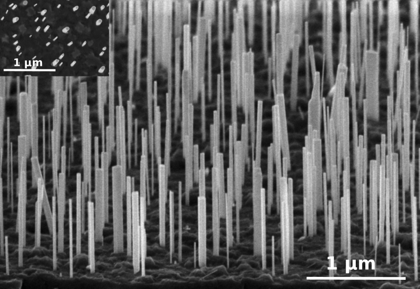
Figure 1 presents a scanning electron microscopy (SEM) micrograph of sample C. A good alignment of the NWs in the direction of the substrate surface normal is clearly seen in the figure and quantified below using XRD. A large roughness of the substrate surface is also evident from the figure, giving rise to an additional scattering in the GISAXS experiment described below. The inset in Fig. 1 shows a scanning electron micrograph of the same sample taken in the direction close to the surface normal. Such images were used to obtain the average NW radii [20] as included in Table 1. However, the resolution of the SEM micrographs is not good enough to reveal details of the cross-sectional shapes of NWs, that we find in the GISAXS study below.
The laboratory XRD measurements are performed in two geometries, out-of-plane in the familiar symmetric Bragg reflection and in-plane at grazing incidence. For the acquisition of out-of-plane reciprocal space maps, we use a Bruker D8 Discover Diffractometer operating a Cu anode at 1.6 kW. The beam conditioning optics are comprised of a Göbel mirror and an asymmetric 2-bounce channel cut Ge (220) monochromator. The beam is thus collimated to about 0.0085∘. The diffracted intensity is recorded using a Mythen 1D position sensitive detector with a channel pitch and width of 50 µm and 8 mm, respectively. The two-dimensional reciprocal space maps are obtained by rocking scans of the sample.
The in-plane XRD measurements are performed using a Rigaku SmartLab high-resolution X-ray diffractometer in a horizontal scattering plane. The source is a 0.48 mm2 electron line focus on a rotating Cu anode operating at 9 kW. The beam is vertically collimated by a Göbel mirror and an asymmetrically cut 2-bounce Ge (220) monochromator is used to select the Cu K emission line. The beam size is reduced to 0.35 mm2 by slits and the angular resolution is defined by horizontal Soller slits of 0.25∘ and 0.228∘ angular acceptance for the incident and scattered beams, respectively. The incidence angle is set to 0.25∘. Diffraction intensities are recorded using a Hypix-3000 area detector with 100100 µm2 pixel size.
Grazing incidence X-ray diffraction (GID) reciprocal space maps are aquired at the beamline ID10 of the European Synchrotron Radiation Facility (ESRF) at an X-ray energy of 22 keV (wavelength Å). A linear detector (Mythen 1K, Dectris) is placed parallel to the substrate surface to cover the range of scattering angles around the diffraction angle of the GaN(100) reflection with . The grazing incidence angle is and the exit angle is . The sample is rotated about the substrate surface normal, and linear detector scans are recorded for different azimuthal angles . The obtained reciprocal space maps are similar to the maps measured in laboratory XRD experiments. We refer to them as the maps, although the sample rotation axis is along the surface normal, in contrast to symmetric Bragg reflections in the laboratory XRD measurements where the sample rotation axis lies in the surface plane.
GISAXS measurements are also performed at the beamline ID10 of ESRF at the same X-ray energy of 22 keV. The incident beam is directed at grazing incidence to the substrate. The grazing angle , presented in Table 1, is chosen for each sample from several trials to provide the best signal from NWs. The critical angle of the total external reflection for Al2O3 at the used energy is . Hence, the angles are at least 2.5 times larger than the critical angle of the substrate, which allows us to avoid possible complications of the scattering pattern typical for grazing incidence X-ray scattering [22]. The X-ray beam incident on the sample is focused by compound refractive lenses to the size at the sample position of 135 µm laterally and 13 µm vertically (in the direction of the surface normal). At an incidence angle of 0.25∘, the size of the spot illuminated by the incident beam at the sample is mm2. With a typical NW density of cm-2, approximately NWs are illuminated simultaneously. A two-dimensional detector (Pilatus 300K, Dectris) is placed at a distance of 2.38 m from the sample. The angular width of a detector pixel is nm-1.
III Results
III.1 XRD
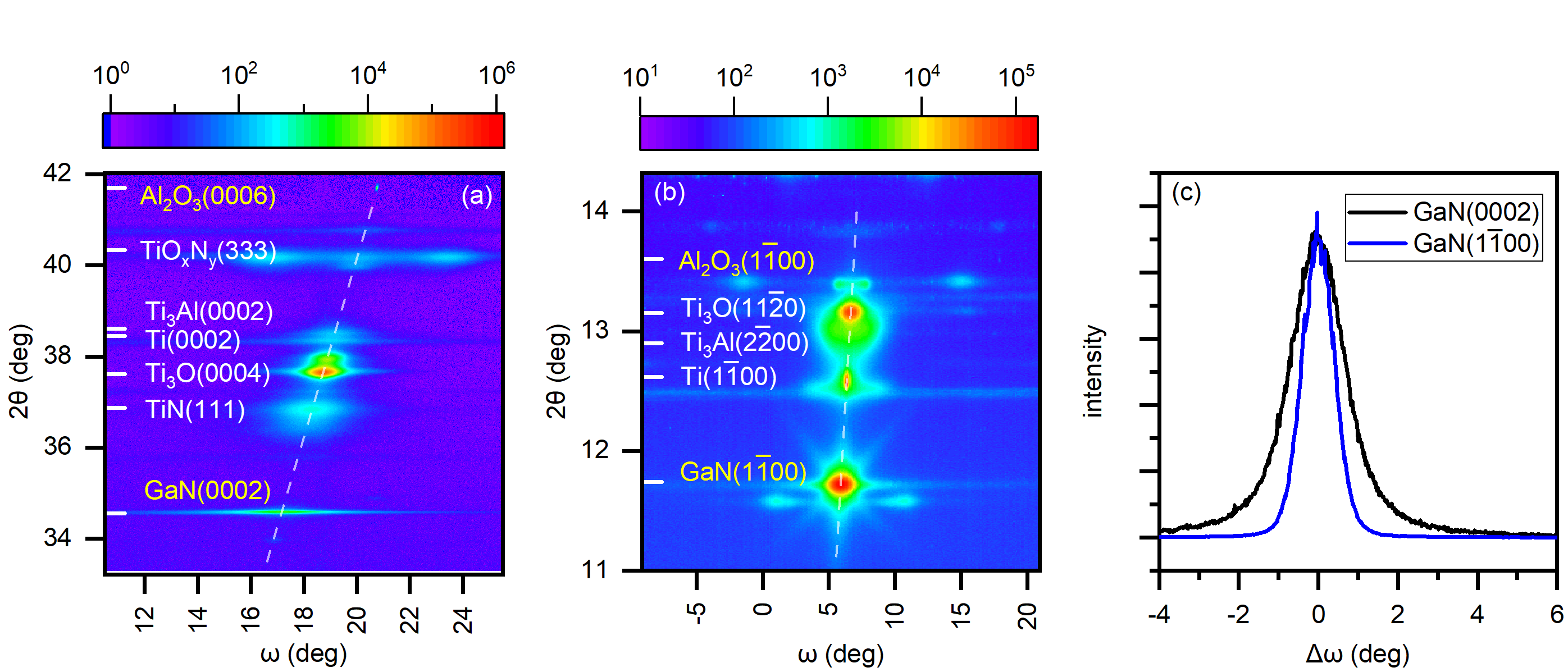
Laboratory XRD measurements of the reciprocal space maps at the GaN(0002) reflection are performed to measure the NW tilt. The maps for samples A–D are very similar. Figure 2(a) presents such a map for sample C. One can see a very sharp Al2O3(0006) reflection and a GaN(0002) reflection that is extended in the direction. An scan through the GaN(0002) reflection, extracted from the map, is shown in Fig. 2(c), yielding the NW tilt, i. e., the FWHM of the NW out-of-plane orientation distribution of 1.52∘. Similar measurements on the other samples give close results summarized in Table 1.
The dashed line from the Al2O3(0006) to GaN(0002) reflections in Fig. 2(a) indicates the direction of a radial scan. One can see a number of peaks in between. They are the result of the interfacial reactions in the sputtered Ti film [23, 24, 25, 26, 21]. High-resolution transmission electron microscopy has shown that the top 40–80 nm of the Ti film is transformed to TiN by nitridation, so that GaN NWs grow on TiN [21].
We indicate in Fig. 2(a) the angles for plausible compounds and reflections found in Pearson’s Crystal Data [27]. We searched for hexagonal phases, with the basal plane parallel to the substrate surface, of compounds composed of Ti and the chemical elements of the substrate or the NWs. Since positions of the diffraction peaks are affected by thermal strain, epitaxial strain, and also by impurities in the crystals, we do not expect that the values exactly coincide with the literature data. Also, there is a notable scattering in the lattice parameters between results of different studies collected in the database [27]. We also include (111) oriented TiOxNy oxynitrides with rocksalt structure, revealed by X-ray photoelectron spectroscopy in previous studies [28, 29, 14], and with a lattice parameter only weakly depending on and [27]. The strongest reflection in Fig. 2(a) is Ti3O(0004). It possesses a width in direction of 0.5∘, i.e., the tilt of the Ti3O crystallites is three times smaller compared to that of the GaN NWs.
Figure 2(b) shows the GID map in the vicinity of the GaN() reflection of the same sample C. Upon rotation of the sample about the surface normal, the diffraction pattern of Fig. 2(b) is repeated after every 60[20]. The dashed line represents the scan. The Al2O3() substrate reflection is not seen because the small incidence and exit angles prevent the penetration of the x-ray radiation into the substrate. This reflection is observed in a measurement with larger incidence and exit angles (not shown here). The scattering angles of the same phases as in Fig. 2(a) are indicated. We find the in-plane reflections of the hexagonal crystals Ti, Ti3O, and Ti3Al. The cubic TiN does not have a Bragg reflection in the angular range of the map in Fig. 2(b).
The -scan through the GaN() reflection is presented in Fig. 2(c). Its FWHM yields the NW twist, i. e., the NW in-plane orientation distribution width, of 0.96∘. For a comparison, the measurement of the same reflection by triple-crystal diffraction at the laboratory diffractometer gives a somewhat smaller value of 0.89∘. The difference can be explained by the geometrical broadening in the synchrotron measurement with the linear detector. In the latter measurement, an mm long stripe on the sample surface is illuminated by the incident X-ray beam and contributes to diffraction. Hence, the twist values obtained by the laboratory X-ray diffraction are more reliable and are given in Table 1.
III.2 GISAXS
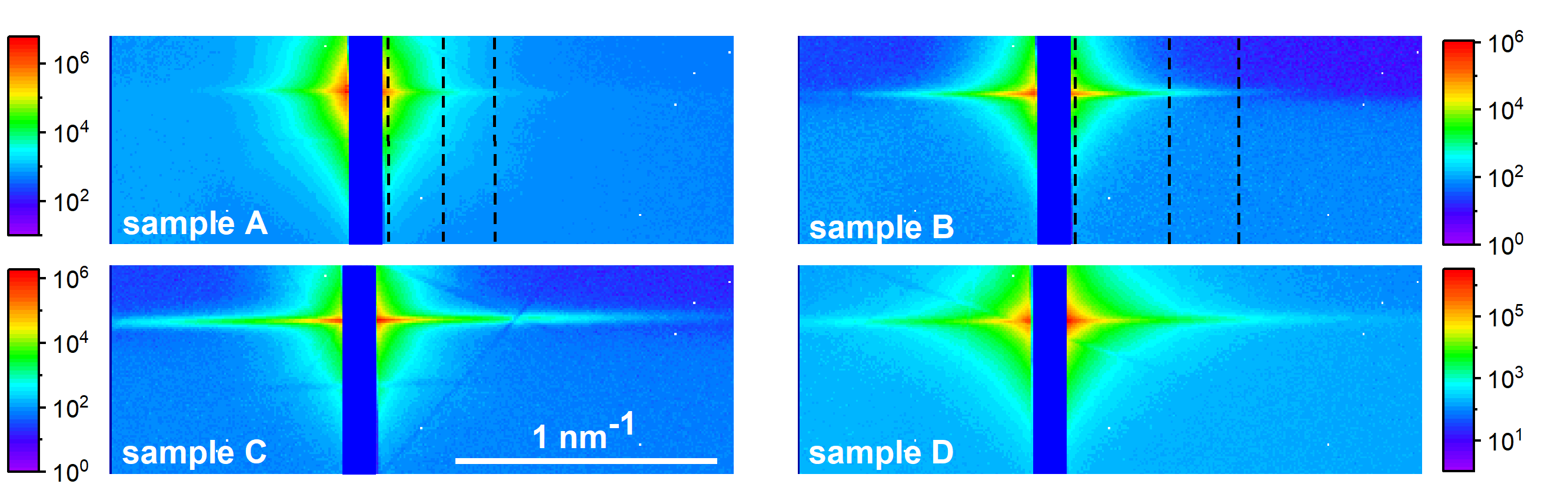
Figure 3 presents the GISAXS intensity distributions around the transmitted beam for samples A–D. Since the GISAXS experiment is intentionally performed with the incidence angles exceeding at least 2.5 times the critical angle for the substrate (see Table 1), the small-angle X-ray scattering patterns comprise three separate regions: around the transmitted beam, around the beam reflected from the substrate, and the Yoneda streak (see Fig. 2 in Ref. [18]). We choose for the analysis the scattering around the transmitted beam, since it is more intense. One can see on each map in Fig. 3 a horizontal (parallel to the substrate surface and normal to the long NW axis) streak and a halo around the direct beam direction. The streak is due to scattering from NWs: the NWs are long rods that scatter in the plane perpendicular to the rods. The halo stems from the scattering from the sputtered film on the substrate.
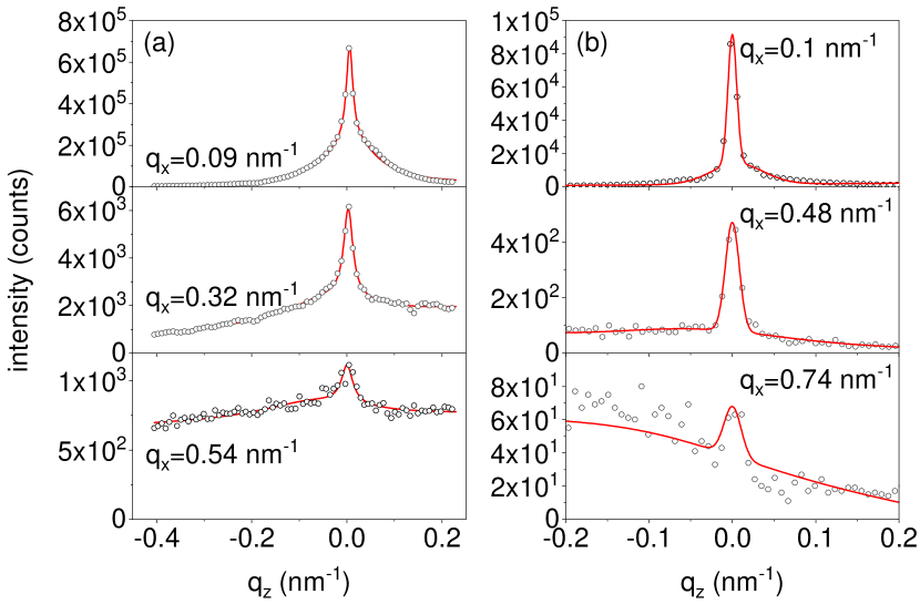
These two contributions to the scattered intensity can be distinguished by analyzing the scans in the surface normal direction. Some exemplary scans are marked in Fig. 3 by dashed lines and the intensity in these scans is shown in Fig. 4. Here, and are parallel to the substrate surface and normal to it, respectively. The scans are fitted to a sum of two Gaussians, a narrow one representing the X-ray scattering intensity from the NWs and a broad one due to the X-ray scattering from the sputtered film, plus a background that linearly depends on . Since each NW scatters in the plane perpendicular to its long axis, a range of orientations of the long axes (tilt) gives rise to a fan in the intensity distribution. Hence, the full width at half maximum (FWHM) of a -scan of the intensity is expected to depend linearly on . The dependencies obtained from the fits of the -scans for samples A–D are presented in Fig. 5. The expected linear dependence is observed. Figure 5 also contains the respective data for GaN NWs on Si(111) [18].
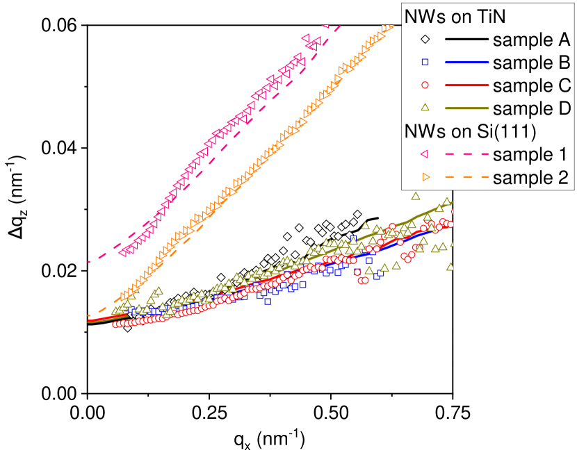
The lines in Fig. 5 are the result of a Monte Carlo simulation that takes into account the distributions of the NW cross-sectional sizes, lengths, and orientations [18]. We simulate the dependence of the scattered intensity at a given and then fit this curve to a Gaussian, in the same way as it is done with the experimental data. The dependence of the FWHM of the Gaussians is close to straight lines, whose slopes depend on the width of the distribution of the NW tilt angles. The tilt angles obtained by adjusting the simulated curves to the experimental ones are presented in Table 1.
The width at has been treated in Ref. [18] as a broadening solely due to the finite NW lengths , . The lengths thus obtained were found to be smaller than the actual NW lengths and attributed to the lengths of the segments of bundled NWs between the joints. In the present case of low NW density, the NWs are not bundled, and their lengths, obtained from the side view SEM micrographs and given in Table 1, are used as an input in the Monte Carlo simulation. We find in the simulation, that the finite-length broadening at is notably smaller than the widths found in the experiment. Then, we take into consideration a finite resolution of the experimental curves and accordingly perform an average of the Monte Carlo intensities in a range . The curves presented in Fig. 5 are obtained with the resolution nm-1, which is 1.5 times the angular size of the detector pixel. This result can be considered as a partial exposure of the neighbor detector pixels. Thus, the curves in Fig. 5 are obtained taking into account both the finite-length and the resolution broadening of the Monte Carlo simulated curves.
We reproduce in Fig. 5 also the experimental data for the GISAXS intensity from GaN NWs on Si(111) [18] and perform new Monte Carlo simulations, which now include the NW lengths taken from the SEM micrographs and the resolution obtained above. The width at for the 230 nm long NWs in sample 1 is mainly due to finite-length broadening, while the respective width for the 650 nm long NWs in sample 2 is mainly due to the finite resolution.
It is evident from comparison of the slopes of the curves in Fig. 5, that the NWs on Ti/Al2O3 show a notably narrower orientation distribution compared to the NWs on Si(111). The widths of the tilt angle distributions obtained from Fig. 5 are found to range from 1.7∘ to 2.3∘ for samples A–D (see Table 1), while for NWs on Si(111), they amount to 5.1∘ and 4.9∘ for samples 1 and 2, respectively.
For further analysis, we need the GISAXS intensity along the horizontal stripes in the reciprocal space maps in Fig. 3. These stripes correspond to the maximum intensity of the -scans exemplified in Fig. 4, with the background scattering subtracted. We use the established linear dependence of the widths on in Fig. 5 to improve the fits of the -scans and extend the -range as much as possible to the regions of low intensity and substantial noise in the experimental data (see the bottom curves in Fig. 4). After a fit of the -scans from a reciprocal space map is performed and the widths obtained, the dependence , shown in Fig. 5, is fitted by a straight line. Then, the fit of the -scans is repeated, now with the peak position and width thus predefined, rather than to be free parameters of the fit. Since the only output of this second fit that we need is the maximum intensity, it can be determined at large , where the experimental data are noisy. The curves shown in Fig. 4 are the result of such two-step fits.
The GISAXS intensity is expected to follow Porod’s law at large , which describes small–angle scattering from any particle with a sharp change of the electron density at the surface [30]. It has the same nature and is as general as Fresnel’s law for scattering from planar surfaces [31]. The epitaxy of GaN NWs to the substrate gives rise to preferential orientations of the side facets and results in an azimuthal dependence of the GISAXS intensity [18].
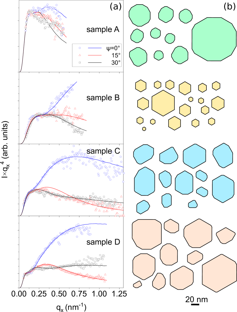
Hence, we plot in Fig. 6 the GISAXS intensity for samples A–D as the product . The reciprocal space maps, similar to the ones presented in Fig. 3, were measured with the azimuthal rotation of the samples about the vertical axis on an angle from to with a step of . The sixfold symmetry of the scattering patterns is established, and the distinct intensity distributions obtained for , , and are shown by circles, triangles, and squares respectively.
We model the GISAXS intensity by the Monte Carlo method, as described in Ref. [18]. The NWs are considered as prisms with polygonal cross sections. Then, the scattered intensity from a single NW can be expressed through the coordinates of the vertexes of the polygon. The simplest shape of the cross section is the a regular hexagon limited by GaN() facets. The hexagon sizes are assumed to obey a lognormal distribution in the Monte Carlo simulations. The calculated intensity curves in Fig. 6 are obtained by averaging the scattering intensity over about NWs generated on random, a number that is an order of magnitude smaller compared to the number of NWs contributing to the measured GISAXS intensity, estimated in Sec. II.
In most cases, regular hexagons are not suitable to model the experimental data. Thus, we first allow a random distortion of the hexagon while keeping the GaN() side facets. Secondly, the vortexes of the hexagons are cut on random by lines with the orientation average of these of the adjoining sides, thus representing GaN() side facets. In this case, the cross-sectional shape of the prism becomes a dodecagon (a polygon with twelve vortices), rather than a hexagon (a polygon with six vortices). The scattered intensity still can be calculated using the positions of the vortices. Lognormal distributions are assumed for the hexagon distortion and for the cuts of its apexes, with the parameters varied to fit the experimental curves. For each simulated polygon, we calculate its area , perimeter , as well as the parts of the perimeter and representing separately () and () facets, . The quantities of interest are the NW radius and the fraction of () facets .
The NW array is simulated by randomly rotating the NWs about the horizontal and vertical axes in angular ranges of the tilt and twist determined by the XRD measurements in Sec. III.1 and presented in Table 1. We also take into account roughness of the side facets of NWs by including random shifts of the side facets in direction of their normals by monolayer height steps. A geometric distribution of steps is assumed and a roughness factor is calculated in the same way as it is done in crystal truncation rod calculations [32]. As a result, the contribution of each facet to the scattering amplitude contains an additional roughness factor [18].
The lines in the plots in Fig. 6(a) are obtained by the Monte Carlo simulation, examples of the simulated cross-sectional shapes are shown in Fig. 6(b), and the parameters of the NW ensembles of the samples A–D are included in Table 1. Let us consider first the GISAXS intensity from sample B. Its dependence on the azimuth is qualitatively similar to that of GaN NWs on Si(111) [18]. The product rises up at large at , decays at , and shows an intermediate behavior at . Such behavior is expected for hexagonal cross sections, and we find that the simulation of NWs by regular hexagons adequately describes the experiment. The maximum intensity at large is the facet truncation rod scattering, and the minimum at is the scattering in the direction of the angle between the facets. The rise of the curve at small is sensitive to the average NW radius, while a dip before further rise of the curve at provides the width of the radial distribution.
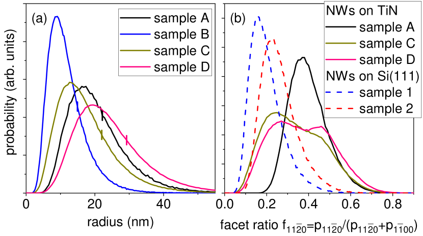
The distribution of the NW radii obtained in the Monte Carlo simulation is shown in Fig. 7(a). We find a mean radius of 11.2 nm and a standard deviation of the radial distribution of 5.2 nm. Sample B exhibits the thinnest NWs from the series under investigation. We also mark by vertical bars on the respective curves in Fig. 7(a) the mean radii obtained in Ref. [20] from top view SEM micrographs and reproduced in Table 1. The mean radii thus obtained are systematically larger by 2 to 5 nm than the ones obtained from GISAXS in the present work. The difference can be partially attributed to the limited resolution of SEM, and partially to asymmetric radii distributions in Fig. 7(a), with the maximum value smaller than the average.
A fine tuning of the Monte Carlo simulations to the experiment also requires to include roughness with an rms value of nm. Since the height of a monolayer step at the side facet of a NW is equal to the GaN lattice parameter nm, this value corresponds to only two atomic steps along the entire NW length.
Proceeding now to sample C, we find that the intensity curve at the intermediate azimuth is not in between the curves for and , as it is expected for oriented hexagons and observed for sample B. Rather, the curves at and almost coincide, and at large the intensity at the azimuth of is even smaller. Simulation of these intensity curves requires to take into account both and side facets. Figure 6 shows the result of the Monte Carlo simulation for sample C and examples of the cross sections used in the simulation. The NW radii are larger, and the radii distribution is broader compared to sample B [see Fig. 7(a)]. The distribution of the fraction is shown in Fig. 7(b). A wide distribution of the ratios of different facets is needed to model the experimental curves. For a comparison, dashed lines in Fig. 7(b) show the facet fractions obtained in the modeling of the GaN NWs on Si(111) [19]. For NWs on Si(111), the facets are present in much smaller amounts.
Turning now to sample D, one can see in Fig. 6 that the curves at the sample orientations and are swapped in comparison to sample B: the intensity at the intermediate orientation (red triangles) is minimum and not intermediate as it is for sample B. A good agreement of the experimental curves and the Monte Carlo modeling of the intensity curves for sample D is reached only with an even broader variation of the facet ratio, see Fig. 7(b). A double-humped distribution of the facet ratio for this sample seems an artifact of the modeling of the cross sections by first producing hexagons and then cutting the corners to obtain dodecagons. The NW radii for sample D are largest in the series [see Fig. 7(a)]. Comparing the average radii and the widths of their distributions in Table 1, one can see that the relative widths of the distributions (the ratios of the standard deviation to the mean value) for samples B–D are close.
Comparing now the intensity curves for sample A in Fig. 6 with these for samples B–D, one can see that the difference between the curves for different sample orientations is notably weaker, and that the product decreases at large significantly faster. A weak orientation dependence implies roundish NW shapes, and such shapes are obtained in the Monte Carlo modeling, see Fig. 6(b). A fast intensity decay is a consequence of a large roughness of the side facets. The modeling gives the roughness nm, notably larger than those for samples B–D (see Table 1).
IV Discussion
GaN NWs grown on 3.4 µm thick Ti films sputtered on Al2O possess remarkably small misorientation ranges, less than 2∘ out-of-plane (tilt) and less than 1∘ in-plane (twist), see Table 1. For comparison, GaN NWs grown on the most common substrate Si(111) exhibit 3–5∘ tilt and twist [33, 2, 18] because of the formation of an amorphous SiNx film, just a few nanometers in thickness, on the Si surface. The other extreme is the epitaxial growth of GaN NWs on AlN/6H-SiC with a tilt and twist of 0.4∘ and 0.6∘, respectively [34].
The XRD reciprocal space maps in Fig. 2(a,b) show that, as a result of the interfacial reactions between Ti and Al2O the sputtered homogeneous Ti film transforms into a heterogeneous alloy containing topotaxial crystallites of Ti, Ti3Al, and Ti3O. These crystals possess hexagonal symmetry, (0001) orientation, and lattice parameters intermediate between those of Al2O3 and GaN. They are topotaxially oriented with respect to the substrate with a misorientation of less than 1∘. The cubic TiOxNy oxynitrides are also found in the film. Simultaneously with the reaction of Ti with the Al2O3 substrate, the top 40–80 nm of the Ti film are converted to cubic TiN, on which the NW growth takes place [21].
The GISAXS measurements and their Monte Carlo modeling allow us to determine the distributions of the NW radii and their cross-sectional shapes, as well as the roughness of their side facets. NWs of sample A, grown on a 1.3 µm thick Ti film, possess roundish cross-sectional shapes and a relatively large roughness of the side facets. Sample A also exhibits blueshifted and broadened photoluminescence spectra as compared to reference GaN NWs, which was attributed to the incorporation of O atoms (diffusing from the Al2O3 substrate at the employed GaN growth temperature), resulting in a background doping high enough to screen excitons and induce bandgap renormalization and band-filling [21]. We thus speculate that the presence of O adatoms at the NW sidewalls may modify their surface energy, giving rise to the presence of both and facets. To reduce this interdiffusion, further samples were grown on 3.4 µm thick Ti films [21].
We find that the roughness of the side NW facets of samples B–D is at least twice smaller than that of sample A. However, the XRD measurements do not show a notable difference in the reciprocal space maps between the samples. The XRD peaks from Ti3O remain the most intense ones both in the symmetric reflection in Fig. 2(a) and in the grazing incidence reflection in Fig. 2(b). We note that the latter measurement reveals the structure of the top part of the layer, due to small incidence and exit angles close to the critical angle of total external reflection. Hence, O still diffuses through the whole Ti layer despite its increased thickness. Regarding the NW shape, only sample B (even grown at the highest temperature) exhibits purely hexagonal NW cross sections, while samples C and D are again characterized by the coexistence of and facets. Furthermore, samples B–D display narrow excitonic transitions in their photoluminescence spectra [20], ruling out the incorporation of O exceeding a concentration of at most cm-3. Our speculation above that O adatoms at the NW sidewalls may modify their surface energy is clearly not supported by these experimental facts.
A recent transmission electron microscopy study of GaN NWs on Si(111) revealed a transformation of the cross-sectional shapes of NWs during their growth [19]. The NWs possess hexagonal cross sections with side facets in their top parts. During growth, their bottom parts attain roundish shapes with both and side facets present. The hexagonal shapes in the top parts are considered as the equilibrium growth shape under the impinging Ga and N fluxes, while the roundish shapes in the bottom parts are understood to reflect a transformation to the equilibrium crystal shape when the side NW surface is shadowed from the impinging fluxes. Since the density of the GaN NWs on TiN studied in the present work is at least one order of magnitude lower compared to GaN NWs on Si(111), the NWs receive impinging fluxes along their whole length, i. e., the mechanism considered for GaN NWs on Si(111) cannot be invoked to explain the roundish shape of the NWs and the presence of facets.
A radically different possibility arises from the incorporation of substantial amounts of Ga prior to GaN growth into the Ti layer [21]. After the growth and during cooling, some of the Ga may be released from the Ti layer due to the reduced solubility at lower temperatures. This Ga wets the GaN NWs and turns into GaOx upon air exposure. We note that the GISAXS intensity depends only on the density of the matter and does not depend on its crystallinity. Since crystalline GaN and amorphous GaOx have close densities, the cross-sectional shapes obtained in Fig. 6(b) are the ones of the NWs covered with the GaOx shell, if the latter is present. The roughness obtained from the GISAXS study also applies the outer NW surface. The roundish shape and the coexistence of and facets would thus be a characteristics of the GaOx shell, while the GaN core may very well have regular hexagonal shape. Plan-view transmission electron microscopy and electron dispersive x-ray spectroscopy could be used to refute or confirm this hypothesis.
V Summary
The diffusion of Al and O from the Al2O3 substrate to the sputtered Ti film gives rise to topotaxial crystallites of Ti, Ti3Al, and Ti3O possessing very little misorientation with respect to the substrate. GaN NWs grown on this film are epitaxially oriented with respect to the substrate notably better compared to GaN NWs on Si(111).
The GISAXS intensity together with its Monte Carlo modeling is capable to provide detailed information on the NW arrays, particularly the distributions of the cross-sectional sizes of the NWs, the fractions of the and side facets, and the roughness of these facets. The NW radii obtained from GISAXS are systematically smaller by 2 to 5 nm compared to the ones obtained from SEM micrographs. The fraction of the facets is notably larger compared to GaN NWs on Si(111), so that the NWs have roundish cross-sectional shape. An exclusion is the sample grown at the a highest temperature. The GISAXS intensity is highly sensitive to the roughness of the side facets, a parameter hardly accessible by any other method. We find that the roughness of the micron long side facets does not exceed the height of 2–3 atomic steps. We propose that both the roughness and the shape are the result of the presence of Ga adatoms at the NW sidewall after growth, and the formation of a GaOx shell upon exposure of the NW to the ambient.
Acknowledgements.
The authors thank R. Volkov and N. Borgardt for fruitful discussions, Thomas Auzelle for critical reading of the manuscript, and the ESRF for the provision of beam time. S. F.-G. acknowledges the partial financial support received through the Spanish program Ramón y Cajal (co-financed by the European Social Fund) under grant RYC-2016-19509 from Ministerio de Ciencia, Innovación y Universidades. He also thanks Universidad Autónoma de Madrid for the transfer to Universidad Politécnica de Madrid of part of the materials and equipment purchased with charge to the RYC -2016-19509 grant.References
- Fernández-Garrido et al. [2009] S. Fernández-Garrido, J. Grandal, E. Calleja, M. A. Sánchez-García, and D. López-Romero, A growth diagram for plasma-assisted molecular beam epitaxy of GaN nanocolumns on Si(111), J. Appl. Phys. 106, 126102 (2009).
- Geelhaar et al. [2011] L. Geelhaar, C. Chèze, B. Jenichen, O. Brandt, C. Pfüller, S. Münch, R. Rothemund, S. Reitzenstein, A. Forchel, T. Kehagias, P. Komninou, G. P. Dimitrakopulos, T. Karakostas, L. Lari, P. R. Chalker, M. H. Gass, and H. Riechert, Properties of GaN nanowires grown by molecular beam epitaxy, IEEE J. Sel. Top. Quantum Electron. 17, 878–888 (2011).
- Ristić et al. [2008] J. Ristić, E. Calleja, S. Fernández-Garrido, L. Cerutti, A. Trampert, U. Jahn, and K. H. Ploog, On the mechanisms of spontaneous growth of III-nitride nanocolumns by plasma-assisted molecular beam epitaxy, J. Cryst. Growth 310, 4035–4045 (2008).
- Sibirev et al. [2012] N. V. Sibirev, M. Tchernycheva, M. A. Timofeeva, J.-C. Harmand, G. E. Cirlin, and V. G. Dubrovskii, Influence of shadow effect on the growth and shape of InAs nanowires, J. Appl. Phys. 111, 104317 (2012).
- Sabelfeld et al. [2013] K. K. Sabelfeld, V. M. Kaganer, F. Limbach, P. Dogan, O. Brandt, L. Geelhaar, and H. Riechert, Height self-equilibration during the growth of dense nanowire ensembles: Order emerging from disorder, Appl. Phys. Lett. 103, 133105 (2013).
- Kaganer et al. [2016] V. M. Kaganer, S. Fernández-Garrido, P. Dogan, K. K. Sabelfeld, and O. Brandt, Nucleation, growth and bundling of GaN nanowires in molecular beam epitaxy: Disentangling the origin of nanowire coalescence, Nano Lett. 16, 3717–3725 (2016).
- ATM G. Sarwar et al. [2015] ATM G. Sarwar, S. D. Carnevale, F. Yang, T. F. Kent, J. J. Jamison, D. W. McComb, and R. C. Myers, Semiconductor nanowire light-emitting diodes grown on metal: A direction toward large-scale fabrication of nanowire devices, Small 11, 5402–5408 (2015).
- Wölz et al. [2015] M. Wölz, C. Hauswald, T. Flissikowski, T. Gotschke, S. Fernández-Garrido, O. Brandt, H. T. Grahn, L. Geelhaar, and H. Riechert, Epitaxial growth of GaN nanowires with high structural perfection on a metallic TiN film, Nano Lett. 15, 3743–3747 (2015).
- Zhao et al. [2016] C. Zhao, T. K. Ng, N. Wei, A. Prabaswara, M. S. Alias, B. Janjua, C. Shen, and B. S. Ooi, Facile formation of high-quality InGaN/GaN quantum-disks-in-nanowires on bulk-metal substrates for high-power light-emitters, Nano Lett. 16, 1056–1063 (2016).
- van Treeck et al. [2018] D. van Treeck, G. Calabrese, J. Goertz, V. Kaganer, O. Brandt, S. Fernández-Garrido, and L. Geelhaar, Self-assembled formation of dense ensembles of long, thin, and uncoalesced GaN nanowires on crystalline TiN films, Nano Res. 11, 565–576 (2018).
- Mudiyanselage et al. [2020] K. Mudiyanselage, K. Katsiev, and H. Idriss, Effects of experimental parameters on the growth of GaN nanowires on Ti-film/Si(100) and Ti-foil by molecular beam epitaxy, J. Cryst. Growth 547, 125818 (2020).
- Calabrese et al. [2016] G. Calabrese, P. Corfdir, G. Gao, C. Pfüuller, A. Trampert, O. Brandt, L. Geelhaar, and S. Fernández-Garrido, Molecular beam epitaxy of single crystalline GaN nanowires on a flexible Ti foil, Appl. Phys. Lett. 108, 202101 (2016).
- May et al. [2016] B. J. May, A. T. M. G. Sarwar, and R. C. Myers, Nanowire LEDs grown directly on flexible metal foil, Appl. Phys. Lett. 108, 141103 (2016).
- Calabrese et al. [2017] G. Calabrese, S. V. Pettersen, C. Pfüller, M. Ramsteiner, J. K. Grepstad, O. Brandt, L. Geelhaar, and S. Fernández-Garrido, Effect of surface roughness, chemical composition, and native oxide crystallinity on the orientation of self-assembled GaN nanowires on Ti foils, Nanotechnology 28, 425602 (2017).
- Ramesh et al. [2019] C. Ramesh, P. Tyagi, G. Abhiram, G. Gupta, M. S. Kumar, and S. S. Kushvaha, Role of growth temperature on formation of single crystalline GaN nanorods on flexible titanium foil by laser molecular beam epitaxy, J. Cryst. Growth 509, 23–28 (2019).
- Ramesh et al. [2020] C. Ramesh, P. Tyagi, J. Kaswan, B. S. Yadav, A. K. Shukla, M. S. Kumar, and S. S. Kushvaha, Effect of surface modification and laser repetition rate on growth, structural, electronic and optical properties of GaN nanorods on flexible Ti metal foil, RSC Adv. 10, 2113–2122 (2020).
- Auzelle et al. [2021] T. Auzelle, M. Azadmand, T. Flissikowski, M. Ramsteiner, K. Morgenroth, C. Stemmler, S. Fernández-Garrido, S. Sanguinetti, H. T. Grahn, L. Geelhaar, and O. Brandt, Enhanced radiative efficiency in GaN nanowires grown on sputtered TiNx: Effects of surface electric fields, ACS Photonics 8, 1718–1725 (2021).
- Kaganer et al. [2021] V. M. Kaganer, O. V. Konovalov, and S. Fernández-Garrido, Small-angle X-ray scattering from GaN nanowires on Si(111): facet truncation rods, facet roughness, and Porod’s law, Acta Cryst. A 77, 42–53 (2021).
- Volkov et al. [2022] R. Volkov, N. I. Borgardt, O. V. Konovalov, S. Fernández-Garrido, O. Brandt, and V. M. Kaganer, Cross-sectional shape evolution of GaN nanowires during molecular beam epitaxy growth on Si(111), Nanoscale Adv. 4, 562–572 (2022).
- Calabrese et al. [2020] G. Calabrese, D. van Treeck, V. M. Kaganer, O. Konovalov, P. Corfdir, C. Sinito, L. Geelhaar, O. Brandt, and S. Fernández-Garrido, Radius-dependent homogeneous strain in uncoalesced GaN nanowires, Acta Mater. 195, 87–97 (2020).
- Calabrese et al. [2019] G. Calabrese, G. Gao, D. van Treeck, P. Corfdir, C. Sinito, T. Auzelle, A. Trampert, L. Geelhaar, O. Brandt, and S. Fernández-Garrido, Interfacial reactions during the molecular beam epitaxy of GaN nanowires on Ti/Al2O3, Nanotechnology 30, 114001 (2019).
- Renaud et al. [2009] G. Renaud, R. Lazzari, and F. Leroy, Probing surface and interface morphology with grazing incidence small angle x-ray scattering, Surf. Sci. Rep. 64, 255–380 (2009).
- Selverian et al. [1991] J. H. Selverian, F. S. Ohuchi, M. Bortz, and M. R. Notis, Interface reactions between titanium thin films and sapphire substrates, J. Mater. Sci. 26, 6300–6308 (1991).
- Li et al. [1992] X. L. Li, R. Hillel, F. Teyssandier, S. K. Choi, and F. J. J. van Loo, Reactions and phase relations in the Ti–Al–O system, Acta metall. mater. 40, 3149–3157 (1992).
- Koyama et al. [1993] M. Koyama, S. Arai, S.Suenaga, and M. Nakahashi, Interfacial reactions between titanium film and single crystal -Al2O3, J. Mater. Sci. 28, 830–834 (1993).
- Kelkar and Carim [1995] G. P. Kelkar and A. H. Carim, Phase equilibria in the Ti–Al–O system at 945∘c and analysis of Ti/Al2O3 reactions, J.Am. Ceram. Soc. 78, 572–576 (1995).
- [27] P. Villars and K. Cenzual, Pearson’s Crystal Data — Crystal Structure Database for Inorganic Compounds (on CD-ROM), Release 2010/11 (ASM International, Materials Park, Ohio, USA).
- Milošev et al. [1995] I. Milošev, H.-H. Strehblow, B. Navinšek, and M. Metikoš-Huković, Electrochemical and thermal oxidation of TiN coatings studied by XPS, Surf. Interf. Anal. 23, 529 (1995).
- Cheng and Zheng [2007] Y. Cheng and Y. F. Zheng, Surface characterization and mechanical property of TiN/Ti-coated NiTi alloy by PIIID, Surf. Coat. Technol. 201, 6869 (2007).
- Porod [1951] G. Porod, Die Röntgenkleinwinkelstreuung von dichtgepackten kolloiden Systemen. I. Teil, Kolloid Z. 124, 83–114 (1951).
- Sinha et al. [1988] S. K. Sinha, E. B. Sirota, S. Garoff, and H. B. Stanley, X-ray and neutron scattering from rough surfaces, Phys. Rev. B 38, 2297–2311 (1988).
- Robinson [1986] I. K. Robinson, Crystal truncation rods and surface roughness, Phys. Rev. B 33, 3830–3836 (1986).
- Jenichen et al. [2011] B. Jenichen, O. Brandt, C. Pfüller, P. Dogan, M. Knelangen, and A. Trampert, Macro- and micro-strain in GaN nanowires on Si(111), Nanotechnol. 22, 295714 (2011).
- Fernández-Garrido et al. [2014] S. Fernández-Garrido, V. M. Kaganer, C. Hauswald, B. Jenichen, M. Ramsteiner, V. Consonni, L. Geelhaar, and O. Brandt, Correlation between the structural and optical properties of spontaneously formed GaN nanowires: A quantitative evaluation of the impact of nanowire coalescence, Nanotechnol. 25, 455702 (2014).