Spectroscopic imaging ellipsometry of two-dimensional TMDC heterostructures
Abstract
Semiconducting two-dimensional materials and their heterostructures gained a lot of interest for applications as well as fundamental studies due to their rich optical properties. Assembly in van der Waals heterostacks can significantly alter the intrinsic optical properties as well as the wavelength-dependent absorption and emission efficiencies making a direct comparison of e.g. photoluminescence intensities difficult. Here, we determine the dielectric function for the prototypical MoSe2/WSe2 heterobilayer and their individual layers. Apart from a redshift of - of the energetically lowest interband transitions, we find that for larger energies the dielectric function can only be described by treating the van der Waals heterobilayer as a new artificial homobilayer crystal rather than a stack of individual layers. The determined dielectric functions are applied to calculate the Michelson contrast of the individual layers and the bilayer in dependence of the oxide thickness of often used Si/SiO2 substrates. Our results highlight the need to consider the altered dielectric functions impacting the Michelson interference in the interpretation of intensities in optical measurements such as Raman scattering or photoluminescence.
The easily accessible method of cleaving bulk van der Waals (vdW) crystals to thin nano-layers Novoselov et al. (2004) has led to the exploration of an ever expanding number of different 2D materials with a broad range of properties Novoselov et al. (2016). The possibility to combine these materials into vdW heterostructures has lead to new application prospects such as solar energy conversion Nassiri Nazif et al. (2021), solid state lighting Hwangbo et al. (2022), field-effect transistor based sensingChen, Liu, and Mao (2020) or spintronic devices Ahn (2020). Experiments on transition metal dichalcogenide (TMDC) vdW heterostructures opened the avenue towards new fundamental research directions including Moiré excitons Seyler et al. (2019); Tran et al. (2019); Di Huang et al. (2022), single photon emitters Klein et al. (2021); Michaelis de Vasconcellos et al. (2022), Mott-Hubbard physics Li et al. (2021) or excitonic many-body states Wang et al. (2019); Sigl et al. (2020). For both, applications as well as fundamental studies, a detailed knowledge of the modifications of the light-matter interaction described by the complex dielectric function in vdW heterostructures compared to the individual layers is important. The dielectric function can be determined by reflectance contrast and Kramers-Kronig constraint analysis Li et al. (2014) as well as by spectroscopic imaging ellipsometry (SIE) Fujiwara (2007). Unlike reflectance contrast, SIE provides access to the dielectric functions also in spectral regions with weak or even no extinction, and the oblique angle of incidence provides access to the in-plane and out-of plane parts of the dielectric tensor Funke et al. (2016). Moreover, experimental determination of the two ellipsometric angles allows a Kramers-Kronig relation free determination of the dielectric functions with both high spatial resolution and a high signal sensitivity by using nulling ellipsometry Fujiwara (2007).
Here, we combine these inherent advantages of spectroscopic imaging ellipsometry with large area vdW heterostructures to study the change in the dielectric function for MoSe2 and WSe2 when assembled in a heterobilayer. We report a redshift of the lowest energy A- and B-exciton resonances in the heterobilayer compared to the individual monolayers. Most strikingly, the higher lying spectral range of the heterobilayer can only be well described by a new material rather than a multilayer system of two stacked monolayers indicating the importance of interlayer hybridization effects. The determined dielectric functions are utilized to calculate the Michelson interference contrast for commonly used Si/SiO2 substrates demonstrating its impact in the evaluation and interpretation of intensities in optical interband experiments such as photoluminescence (PL), absorbance or Raman experiments.
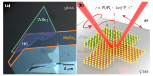
An optical micrograph of the investigated MoSe2/WSe2 heterobilayer is shown in Fig. 1 (a). The bulk crystals (hqgraphene) were cleaved onto the PDMS with Nitto white tape. The monolayers were identified via optical contrast and placed on top of each other on a Borofloat 33 (Schott) silicate glass substrate utilizing a viscoelastic stamping method Castellanos-Gomez et al. (2014).
SIE measurements are performed in ambient condition using an EP4 (Accurion) ellipsometer with a fixed angle of incidence of Funke et al. (2016). The ellipsometer is configured in a polarizer (P), compensator (C), sample (S) and analyzer (A), or so-called PCSA geometry. The measurements are performed in nulling mode Fujiwara (2007), for which elliptically polarized light is created by the P/C-polarizers such that linearly polarized light is reflected from the surface as sketched in Fig. 1 (b). The P- and A-angles are varied with a fixed C-angle to identify the angle configuration resulting in minimal signal on the detector that is either an indivdiual pixel or binned pixels from a charge coupled device (CCD) camera enabling the imaging functionality. The P and A angles for minimal signal determine the ellipsometric angles and , which satisfy the ellipsometric equation for the complex reflectance matrix
| (1) |
with the parallel/orthogonal reflected intensity / normalized to the incident light intensity. In the detection arm, a 50x objective with NA=0.45 is used to image the signal onto the CCD camera providing an overall lateral resolution of the setup of Funke et al. (2016). Tunable and monochromatic illumination is performed by a supercontinuum white light laser combined with acousto-optic tunable filters (AOTF) providing a spectral line-width better than . The accessible spectral range covers () to (). Reflections from the backside of the transparent substrate are suppressed with a beam cutter in the excitation path Funke et al. (2016). Suitable regions of interest (ROIs) are defined on homogeneous regions of the vdW heterobilayer as well as on individual layers. The ROIs allow the measurement of the ellipsometric spectra and with the desired spatial resolution and an optimized signal-to-noise ratio by binning several pixels Funke et al. (2016).
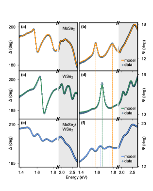
To explore the impact of heterostructuring on the light-matter interaction, we determine the complex dielectric functions of the individual MoSe2, WSe2 monolayers and the combined MoSe2/WSe2 heterobilayer by means of SIE. In order to describe the measured SIE spectra of the monolayer and heterobilayer, a comprehensive optical multilayer model is constructed. A fit procedure via regression analysis allows to extract the dielectric function and thickness for each layer Funke et al. (2016). The multilayer model consists of a glass substrate, the TMDC layer(s) and air. The glass substrate is approximated as a semi-infinite thickness layer with a Cauchy type dielectric function. The TMDC monolayers on top of the substrate are described by a sum of Tauc-Lorentzian and Lorentzian oscillators to account for the excitonic nature of the resonances Funke et al. (2016). Figure 2 provides a comparison of the measured ellipsometric spectra and (grey dots) together with the result from regression analysis (solid lines) allowing to extract the dielectric functions for each constituent layer. We find that in order to achieve good agreement between measured ellipsometric spectra and the fit to the model, the MoSe2/WSe2 heterostructure needs to be modelled as an artificial homobilayer with a model that is partially independent of the individual monolayers. By this approach, we achieve very good agreement between measured data and fit to the model as can be seen in Fig. 2. Minor deviations at the boundaries of the experimentally accessible spectral range can be attributed to out-of-range resonances in the dielectric functions that are included using literature values Kravets et al. (2017). The finding that the vdW heterobilayer cannot be properly described by a multilayer system of two independent monolayers can be explained by significant hybridization effects between the MoSe2 and WSe2 monolayers Gillen and Maultzsch (2018); Kiemle et al. (2020). This is particularly prominent in the higher energy region (above ) (grey regions in Fig. 2). The heterobilayer needs to be treated as a new artificial vdW solid rather than an independent stack of TMDC monolayers. A table containing all fit parameters can be found in the supplementary information.
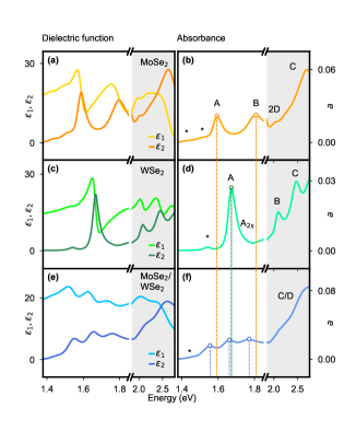
In Fig. 3 (a), (c), (e) the extracted dielectric functions of MoSe2, WSe2 and the MoSe2/WSe2 heterobilayer are plotted, while Fig. 3 (b), (d), (f) display the therefrom deduced absorbance spectra (see supplementary information for details).
The extracted dielectric function of MoSe2 contains two broad and weak sub-gap peaks at and marked with asterisks in Fig. 3 (b) that we attribute to a sub-gap continuum of states related to defect sites Refaely-Abramson et al. (2018). Two strong excitonic resonances are assigned to the A- and B-exciton transition at near the fundamental band-gap from the spin-orbit split bands at the K-points of the Brillouin-zone occurring at and at , respectively. A weaker resonance marked with a 2D at is attributed to an interband transition of an unbound electron-hole pair indicating the fundamental band gap Klein et al. (2019). At higher energies the so called C-exciton signatures originating from band nesting between the M and points of the Brillouin-zone are described by a sum of several smaller excitonic resonances Li et al. (2014); Morozov and Kuno (2015); Hsu et al. (2019).
Analogous to MoSe2, also for WSe2 a weak sub-gap signal related to defects is observed at (cf. Fig. 3 (d)). The A-exciton energy is at and the B-exciton can be seen at . A signature of the fundamental band gap is expected at approximately and not resolvable since it is superimposed by the B-exciton Heißenbüttel et al. (2021). An additional peak between the A- and B-exciton at can be interpreted as the first excited Rydberg state A2s Chernikov et al. (2014). In contrast to MoSe2, the C-exciton is well described by a single peak at . The fit to the data reveals signatures of the energetically higher-lying D-exciton at approximately even though this excitonic resonance is not within the directly accessible experimental range.
Similar to the constituent monolayers, the sub-gap part of the dielectric function of the MoSe2/WSe2 heterobilayer is best described by a weak, defect related peak at (cf. Fig. 3 (f)). The three distinct peaks in the A/B-exciton spectral range between and are attributed to the A-exciton of MoSe2 at , the A-exciton of WSe2 at and the B-exciton of MoSe2 at . The observed redshift of the signatures in comparison to the monolayers are indicated by dashed lines in Fig. 3 (f). The A/B-excitons of MoSe2 shift by about and , respectively. The shift of the A-exciton of WSe2 is , while the B-exciton is superimposed by higher lying transitions and no longer clearly resolvable. These observed redshifts are consistent with photoluminescence studies on this material system Rigosi et al. (2015) and are supposed to be caused by a modified dielectric environment which, combined with layer hybridization, reduces the exciton binding energies Chernikov et al. (2014); Raja et al. (2017) and stimulates band gap renormalization Rigosi et al. (2015) due to the transition from monolayer to heterobilayer. As demonstrated above, energetically higher lying transitions lose the single monolayer character and can only be described by a new homogeneous layer with the thickness of the heterobilayer. This result suggests strong hybridization between the two layers, resulting in a delocalization of the electronic states in the heterobilayer, making a description as new artificial vdW solid necessary Gillen and Maultzsch (2018); Kiemle et al. (2020). The dielectric function in the C/D-exciton spectral range of the individual monolayers is well described by new interband transitions between the hybridized electronic bands of the new vdW solid formed by the MoSe2/WSe2 heterobilayer. Access to the data sets are provided in the supplementary information as a separate text file.
Next, we utilized the obtained dielectric functions to model the Fresnel-based modifications of the reflectance contrast of individual films and MoSe2/WSe2 heterobilayers on commonly used Si/SiO2 substrate materials. The modified interaction with light of the 2D material on a substrate is an important parameter to consider for both the identification by optical contrast as well as optical experiments including reflectance measurements, PL- and Raman-spectroscopy. These modifications are based on the dielectric functions and thicknesses of the investigated multilayer system and therefore have a strong dispersion, making it difficult to e.g. interpret and compare intensities in optical experiments such as the quenching of intralayer excitons which is often considered since it serves as a fingerprint for strong interlayer couplingDeilmann, Rohlfing, and Wurstbauer (2020).
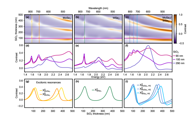
To this end, we employ a plane-wave transfer matrix model to provide the framework of description for the optical response of a multilayer thin film dielectric system Yeh (ting); Teo et al. (2008). As base layer, the common Si/SiO2 substrate is used with literature dielectric functions Malitson (1965); Green (2008). The Si-layer is treated as semi-infinite. For the TMDCs on top, the dielectric functions obtained from our ellipsometry measurements (cf. Fig. 3) are used in the calculation. The Michelson contrast can be calculated from the obtained reflectivity by .
Figure 4 (a) - (c) depict the calculated contrast in dependence of the SiO2-thickness between and and as a function of the experimentally relevant wavelength range from to . Warmer colors indicate a positive contrast, while colder colors indicate a negative contrast. For all three layer configurations, the excitonic features of the dielectric functions presented in Fig. 3 are clearly visible. The horizontal lines indicate three of the most broadly used SiO2-thicknesses in the 2D community, in particular , and . Figure 4 (d) - (f) presents the contrast curves for those substrates. Both the and SiO2 layers provide reasonable contrast for MoSe2 and WSe2 as well as their heterostructure, with clearly distinguishable excitonic features. Substrates with a thick SiO2 layer have a significantly larger contrast in the sub spectral range. The very commonly used oxide-layer establishes itself as a suitable substrate for the identification of MoS2 and WS2. However, for the MoSe2/WSe2 heterobilayer investigated in this work, this oxide thickness yields a very poor contrast in the above spectral range where interlayer exciton emission is dominant, with the excitonic features having very weak intensities due to destructive interference in the multilayer system in all optical experiments. This result highlights the importance of the choice of the substrate for a specific experiment. The impact of the Fresnel interference in a certain spectral range dominated by the substrate and the whole multilayer structure has to be taken into account for the evaluation of the intensities of the absorbed as well as emitted or scattered light. Since many optical experiments are carried out with detection and excitation in the spectral range of the A and B excitonic resonances of the TMDCs, Fig. 4 (g) - (i) gives an overview of the substrate dependence on the contrast for the respective excitonic resonances. The spectral cuts are indicated by horizontal lines in Fig. 4 (a) - (c). Optimal performance can be achieved by using either an oxide thickness around or around to .
Many experiments compare absolute intensities in reflectance, PL- and Raman-spectroscopy using either excitation and/or detection with different light wavelengths. In both cases our simulations demonstrate the sine qua non of taking the choice of substrate into account in the interpretation of the data. Substrate effects can cause variations in the light absorption or emission intensities of much more than an order of magnitude without any intrinsic changes of the light-matter interaction of the investigated materials. With the experimentally determined dielectric functions in particular in the spectral range of the vdW solid that cannot be described by the individual monolayer, our results indicate a guide for better identification and hence fabrication of complex vdW heterostructures. The simulations of the interference contrast can easily be extended to more complex heterostacks including e.g. hBN and graphene for encapsulation and gating Novoselov et al. (2016); Kiemle et al. (2020). We demonstrate that it is important to separate intrinsic modification of the light-matter interaction from extrinsic intensity effects due to substrates and multilayer structures that can vary significantly in different spectral ranges e.g. by comparison of intensities of interlayer and intralayer excitons as a signature for interlayer coupling or evaluation of off- and on-resonant excitation in emission or Raman experiments.
Acknowledgements.
The authors acknowledge the financial support by the Deutsche Forschungsgemeinschaft (DFG) via priority program 2244 (2DMP), via cluster of excellence e-Conversion (EXC 2089/1-390776260) and individual projects HO 3324 / 9-2 and WU 637 / 4-2 and 7-1. J.K. acknowledges support by the Alexander von Humboldt foundation.Data Availability Statement
References
- Novoselov et al. (2004) K. S. Novoselov, A. K. Geim, S. V. Morozov, D. Jiang, Y. Zhang, S. V. Dubonos, I. V. Grigorieva, and A. A. Firsov, “Electric field effect in atomically thin carbon films,” Science 306, 666–669 (2004).
- Novoselov et al. (2016) K. S. Novoselov, A. Mishchenko, A. Carvalho, and A. H. Castro Neto, “2D materials and van der Waals heterostructures,” Science (New York, N.Y.) 353, aac9439 (2016).
- Nassiri Nazif et al. (2021) K. Nassiri Nazif, A. Daus, J. Hong, N. Lee, S. Vaziri, A. Kumar, F. Nitta, M. E. Chen, S. Kananian, R. Islam, K.-H. Kim, J.-H. Park, A. S. Y. Poon, M. L. Brongersma, E. Pop, and K. C. Saraswat, “High-specific-power flexible transition metal dichalcogenide solar cells,” Nature Communications 12, 7034 (2021).
- Hwangbo et al. (2022) S. Hwangbo, L. Hu, A. T. Hoang, J. Y. Choi, and J.-H. Ahn, “Wafer-scale monolithic integration of full-colour micro-LED display using MoS2 transistor,” Nature Nanotechnology , 1–7 (2022).
- Chen, Liu, and Mao (2020) X. Chen, C. Liu, and S. Mao, “Environmental analysis with 2D transition-metal dichalcogenide-based field-effect transistors,” Nano-Micro Letters 12, 95 (2020).
- Ahn (2020) E. C. Ahn, “2D materials for spintronic devices,” npj 2D Materials and Applications 4, 1–14 (2020).
- Seyler et al. (2019) K. L. Seyler, P. Rivera, H. Yu, N. P. Wilson, E. L. Ray, D. G. Mandrus, J. Yan, W. Yao, and X. Xu, “Signatures of moiré-trapped valley excitons in MoSe2/WSe2 heterobilayers,” Nature 567, 66–70 (2019).
- Tran et al. (2019) K. Tran, G. Moody, F. Wu, X. Lu, J. Choi, K. Kim, A. Rai, D. A. Sanchez, J. Quan, A. Singh, J. Embley, A. Zepeda, M. Campbell, T. Autry, T. Taniguchi, K. Watanabe, N. Lu, S. K. Banerjee, K. L. Silverman, S. Kim, E. Tutuc, L. Yang, A. H. MacDonald, and X. Li, “Evidence for moiré excitons in van der Waals heterostructures,” Nature 567, 71–75 (2019).
- Di Huang et al. (2022) Di Huang, J. Choi, C.-K. Shih, and X. Li, “Excitons in semiconductor moiré superlattices,” Nature Nanotechnology 17, 227–238 (2022).
- Klein et al. (2021) J. Klein, L. Sigl, S. Gyger, K. Barthelmi, M. Florian, S. Rey, T. Taniguchi, K. Watanabe, F. Jahnke, C. Kastl, V. Zwiller, K. D. Jöns, K. Müller, U. Wurstbauer, J. J. Finley, and A. W. Holleitner, “Engineering the luminescence and generation of individual defect emitters in atomically thin MoS2,” ACS Photonics 8, 669–677 (2021).
- Michaelis de Vasconcellos et al. (2022) S. Michaelis de Vasconcellos, D. Wigger, U. Wurstbauer, A. W. Holleitner, R. Bratschitsch, and T. Kuhn, “Single-photon emitters in layered van der Waals materials,” physica status solidi (b) 259, 2100566 (2022).
- Li et al. (2021) T. Li, S. Jiang, L. Li, Y. Zhang, K. Kang, J. Zhu, K. Watanabe, T. Taniguchi, D. Chowdhury, L. Fu, J. Shan, and K. F. Mak, “Continuous mott transition in semiconductor moiré superlattices,” Nature 597, 350–354 (2021).
- Wang et al. (2019) Z. Wang, D. A. Rhodes, K. Watanabe, T. Taniguchi, J. C. Hone, J. Shan, and K. F. Mak, “Evidence of high-temperature exciton condensation in two-dimensional atomic double layers,” Nature 574, 76–80 (2019).
- Sigl et al. (2020) L. Sigl, F. Sigger, F. Kronowetter, J. Kiemle, J. Klein, K. Watanabe, T. Taniguchi, J. J. Finley, U. Wurstbauer, and A. W. Holleitner, “Signatures of a degenerate many-body state of interlayer excitons in a van der Waals heterostack,” Physical Review Research 2, 042044 (2020).
- Li et al. (2014) Y. Li, A. Chernikov, X. Zhang, A. Rigosi, H. M. Hill, A. M. van der Zande, D. A. Chenet, E.-M. Shih, J. Hone, and T. F. Heinz, “Measurement of the optical dielectric function of monolayer transition-metal dichalcogenides: MoS2, MoSe2, WS2, and WSe2,” Physical Review B 90 (2014), 10.1103/PhysRevB.90.205422.
- Fujiwara (2007) H. Fujiwara, Spectroscopic ellipsometry: Principles and applications (John Wiley, Chichester, 2007).
- Funke et al. (2016) S. Funke, B. Miller, E. Parzinger, P. Thiesen, A. W. Holleitner, and U. Wurstbauer, “Imaging spectroscopic ellipsometry of MoS2,” Journal of physics. Condensed matter : an Institute of Physics journal 28, 385301 (2016).
- Castellanos-Gomez et al. (2014) A. Castellanos-Gomez, M. Buscema, R. Molenaar, V. Singh, L. Janssen, H. S. J. van der Zant, and G. A. Steele, “Deterministic transfer of two-dimensional materials by all-dry viscoelastic stamping,” 2D Materials 1, 011002 (2014).
- Kravets et al. (2017) V. G. Kravets, V. V. Prorok, L. V. Poperenko, and I. A. Shaykevich, “Ellipsometry and optical spectroscopy of low-dimensional family TMDs,” Semiconductor physics, quantum electronics & optoelectronics , 284–296 (2017).
- Gillen and Maultzsch (2018) R. Gillen and J. Maultzsch, “Interlayer excitons in MoSe2/WSe2 heterostructures from first principles,” Physical Review B 97, 165306 (2018).
- Kiemle et al. (2020) J. Kiemle, F. Sigger, M. Lorke, B. Miller, K. Watanabe, T. Taniguchi, A. Holleitner, and U. Wurstbauer, “Control of the orbital character of indirect excitons in MoS2/WoS2 heterobilayers,” Physical Review B 101, 121404 (2020).
- Refaely-Abramson et al. (2018) S. Refaely-Abramson, D. Y. Qiu, S. G. Louie, and J. B. Neaton, “Defect-induced modification of low-lying excitons and valley selectivity in monolayer transition metal dichalcogenides,” Physical Review Letters 121, 167402 (2018).
- Klein et al. (2019) J. Klein, A. Kerelsky, M. Lorke, M. Florian, F. Sigger, J. Kiemle, M. C. Reuter, T. Taniguchi, K. Watanabe, J. J. Finley, A. N. Pasupathy, A. W. Holleitner, F. M. Ross, and U. Wurstbauer, “Impact of substrate induced band tail states on the electronic and optical properties of MoS2,” Applied Physics Letters 115, 261603 (2019).
- Morozov and Kuno (2015) Y. V. Morozov and M. Kuno, “Optical constants and dynamic conductivities of single layer MoS2, MoSe2, and WSe2,” Applied Physics Letters 107, 083103 (2015).
- Hsu et al. (2019) C. Hsu, R. Frisenda, R. Schmidt, A. Arora, S. M. Vasconcellos, R. Bratschitsch, H. S. J. Zant, and A. Castellanos-Gomez, “Thickness-dependent refractive index of 1L, 2L, and 3L MoS2, MoSe2, WS2, and WSe2,” Advanced Optical Materials 7, 1900239 (2019).
- Heißenbüttel et al. (2021) M.-C. Heißenbüttel, T. Deilmann, P. Krüger, and M. Rohlfing, “Valley-dependent interlayer excitons in magnetic WSe2/CrI3,” Nano letters 21, 5173–5178 (2021).
- Chernikov et al. (2014) A. Chernikov, T. C. Berkelbach, H. M. Hill, A. Rigosi, Y. Li, O. B. Aslan, D. R. Reichman, M. S. Hybertsen, and T. F. Heinz, “Exciton binding energy and nonhydrogenic Rydberg series in monolayer WS2,” Physical Review Letters 113, 076802 (2014).
- Rigosi et al. (2015) A. F. Rigosi, H. M. Hill, Y. Li, A. Chernikov, and T. F. Heinz, “Probing interlayer interactions in transition metal dichalcogenide heterostructures by optical spectroscopy: MoS2 /WS2 and MoSe2/WSe2,” Nano letters 15, 5033–5038 (2015).
- Raja et al. (2017) A. Raja, A. Chaves, J. Yu, G. Arefe, H. M. Hill, A. F. Rigosi, T. C. Berkelbach, P. Nagler, C. Schüller, T. Korn, C. Nuckolls, J. Hone, L. E. Brus, T. F. Heinz, D. R. Reichman, and A. Chernikov, “Coulomb engineering of the bandgap and excitons in two-dimensional materials,” Nature Communications 8, 15251 (2017).
- Deilmann, Rohlfing, and Wurstbauer (2020) T. Deilmann, M. Rohlfing, and U. Wurstbauer, “Light-matter interaction in van der Waals hetero-structures,” Journal of physics. Condensed matter : an Institute of Physics journal 32, 333002 (2020).
- Yeh (ting) P. Yeh, Optical waves in layered media, Wiley series in pure and applied optics (Wiley-Interscience, Hoboken, N.J. and Great Britain, 1998 2005 [printing).
- Teo et al. (2008) G. Teo, H. Wang, Y. Wu, Z. Guo, J. Zhang, Z. Ni, and Z. Shen, “Visibility study of graphene multilayer structures,” Journal of Applied Physics 103, 124302 (2008).
- Malitson (1965) I. H. Malitson, “Interspecimen comparison of the refractive index of fused silica,” Journal of the Optical Society of America 55, 1205 (1965).
- Green (2008) M. A. Green, “Self-consistent optical parameters of intrinsic silicon at 300K including temperature coefficients,” Solar Energy Materials and Solar Cells 92, 1305–1310 (2008).