Interlayer excitonic insulator in two-dimensional double-layer semiconductor junctions: An explicitly solvable model
Abstract
Excitonic insulators conduct neither electrons nor holes but bound electron-hole pairs, excitons. Unfortunately, it is not possible to inject and detect the electron and hole currents independently within a single semiconducting layer. However, interlayer excitonic insulators provide a spatial separation of electrons and holes enabling exciton current measurements. The problem is that the spatial separation weakens electron-hole pairing and may lead to interlayer exciton disassociation. Here we develop an explicitly solvable model to determine an interlayer separation that is strong enough to prevent electron and hole hopping across the layers but still allows for electron-hole pairing sufficient for transition into an interlayer excitonic insulator state. An ideal junction to realize such a state would comprise a pair of identical narrow-gap two-dimensional semiconductors separated by a wide-gap dielectric layer with low dielectric permittivity. The present study quantifies parameters of such a junction by taking into account interlayer coherence effects.
I Introduction
The concept of excitonic insulator (EI) dates back to the 60’s when the normal insulating ground state was found to be unstable against the formation of electron-hole bound states (excitons) in semiconductors with a narrow bandgap Keldysh and Kopaev (1965); Cloizeaux (1965); Jérome et al. (1967). The instability emerges as soon as the exciton binding energy exceeds the semiconducting bandgap. The resulting state remains insulating for holes and electrons separately but becomes capable to conduct excitons. Unfortunately, low exciton binding energy and lack of separate control over electron and hole populations conceal manifestations of the EI state in bulk semiconductors Bucher et al. (1991); Cercellier et al. (2007); Wakisaka et al. (2009); Lu et al. (2017); Mor et al. (2017). However, the recent advent of two-dimensional (2D) materials has revived the field and led to the interlayer excitonic insulator (IEI) concept Wu et al. (2019); Chui et al. (2021); Sodemann et al. (2012); Brunetti et al. (2018); Shi et al. (2022); Du et al. (2017); Ma et al. (2021); Zhang et al. (2022).
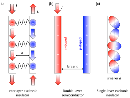
The idea is to make use of a double-layer semiconductor structure with a dielectric spacer that prevents the interlayer electron-hole pairs from recombination but allows for strong Coulomb pairing Ma et al. (2021); Zhang et al. (2022); Wu et al. (2019); Chui et al. (2021); Sodemann et al. (2012); Xie and MacDonald (2018); Brunetti et al. (2018). Besides higher exciton binding energies in 2D semiconductors, the double-layer configuration makes it possible to realize a drag-counterflow setup Su and MacDonald (2008); Eisenstein and MacDonald (2004); Vignale and MacDonald (1996) with two pairs of contacts for independent control of electron and hole transport, see Fig. 1(a). However, the requirements for a suitable dielectric spacer are somewhat contradictory. On the one hand, the electron-hole attraction across the junction must be much weaker than the intralayer confinement to avoid interlayer charge hopping. On the other hand, the electron-hole interactions must be sufficiently strong to ensure stability of the IEI phase state. Indeed, to achieve better interlayer electrical isolation, one could increase the spacer thickness , see Fig. 1(b). However, increasing leads to strong reduction of the bare Coulomb 2D Fourier transform, , by the form-factor , where is the dielectric permittivity of the interlayer media. The reduction is especially strong for larger in-plane wave vectors relevant for tightly bound excitons Trushin (2019). To achieve stronger electron-hole pairing one could decrease , see Fig. 1(c). This increases the interlayer charge hoping probability and gradually reduces the double-layer structure to a bilayer material hosting conventional excitons Jia et al. (2022). Hence, even if the IEI state exists at all, it remains stable only within a certain interval of values limited from below and above by material parameters.
The quantum mechanical effects add even more interesting physics into the IEI problem. The eigenstate of a charge carrier in a double-layer structure obviously does not coincide with that of a separated layer. Once an electron (or a hole) is created in an eigenstate of a given layer its further evolution is governed by the double-layer Hamiltonian. The resulting probability density oscillates between two layers, and at certain time points its maximum occurs on the opposite side of a symmetric double-layer structure. Hence, the electrons and holes injected into the eigenstates of the separated layers can hop between the layers when evolving in time. The phenomenon could be seen as an interlayer coherence that can be suppressed by either the double-layer asymmetry or disorder.
The main question addressed in the present paper is whether the interlayer coherence between electrons and holes is beneficial for bringing them into the IEI state suitable for the drag-counterflow measurements, Fig. 1(a). To answer this question we maximize the coherence effect by employing a perfectly symmetric double-layer structure modeled by a double-delta-shaped out-of-plane confinement. We reveal two competing mechanisms: (i) electron-hole pairing with larger in-plane wave vectors that facilitates transition into the IEI state, and (ii) interlayer hopping that hampers formation of the IEI state. We find the set of parameters at which the mechanism (i) dominates in symmetric double-layer structures and makes transition into the IEI state possible.
The drag-counterflow setup implies no superfluidity that is in line with the Kohn-Sherrington classification Kohn and Sherrington (1970) relating the electron-hole bound complexes to type II bosons. The possibility of exciton condensation and superfluidity in electron-hole double layers has been discussed in Refs. Zhu et al. (1995); Conti et al. (1998).
The paper is organized as follows. Section II introduces the one-particle framework for understanding physics of a double-layer semiconductor junction. Section III builds up with a mean-field theory of electron-hole pairing to describe transition between the normal and IEI states. Section IV provides discussion of asymmetric double-layer structures with different relative permittivities of the dielectric spacer. Section V concludes with a recipe for the IEI using existing 2D materials.
II Single-particle prerequisites
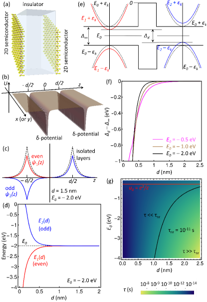
Let us first describe the double-layer junction at a single-particle level. The junction comprises two identical 2D semiconductors separated by a dielectric layer of thickness , see Fig. 2(a,b). Each semiconducting layer is described by the effective low-energy 2D Hamiltonian resulting in the dispersion of a massive Dirac particle Kormányos et al. (2015); Xiao et al. (2012). As the semiconductors are 2D, the out-of-plane confinement must be very narrow for each layer. Such ultimately narrow confinements are conveniently described by the Dirac delta-shaped potentials. Thus, the model Hamiltonian is written as , where
| (1) |
| (2) |
with given by
| (3) |
Here, are the components of the electron momentum operator with being the Planck constant, is the free electron mass, is the band parameter (effective velocity), is the layer confinement parameter, and is the bandgap at .
The in-plane term, , can be deduced from the minimal k.p model describing the coupled dynamics of the valence and conduction bands in 2D transition metal dichalcogenides Kormányos et al. (2015); Xiao et al. (2012). Written in the sublattice basis, the low-energy expansion of the k.p Hamiltonian results in the off-diagonal terms linear in . The spin-orbit splitting, electron–hole asymmetry, and the trigonal warping are neglected here. The out-of-plane electron motion is described by in terms of free electron mass because there is no periodicity along -axis and no effective electron mass can be introduced. However, the out-of-plane motion is restricted by the layer confinement, hence, is not a good quantum number.
The eigenfunctions of can be factorized and written explicitly as . Here, the indices “1,2” stand respectively for the even and odd states, see Fig. 2(c,d), and “” refers to the conduction and valence bands, see Fig. 2(e). The even/odd classification refers only to the symmetric double-layer structures considered in sections II and III. If the symmetry was broken, then the indices “1,2” would respectively refer to the left/right layer of the junction, see section IV. The factorized functions read Santarsiero and Gori (2019); Ahmed et al. (2016)
| (4) |
where ,
| (5) |
with being the Lambert function (ProductLog in Wolfram’s Mathematica), and
| (6) |
| (7) |
where , , , and is the layer size. The corresponding eigenvalues are given by , where
| (8) |
and
| (9) |
with . The two energy branches, , merge to in the limit of , see Fig. 2(d). As decreases, the bands shift in opposite directions forming a type II junction that potentially can host interlayer excitons Özcelik et al. (2016). Note, however, that we consider a homojunction, not a heterostructure Özcelik et al. (2016). The interlayer bandgap reads , see Fig. 2(f). It naturally reduces when the layers get closer to each other. If the Fermi level is fixed, then the left semiconducting layer becomes n-doped, whereas the right one acquires p-doping. Note, that such a doping-by-proximity effect is intrinsic for our model.
The single-particle model is able to indicate the mechanisms that can potentially hamper the IEI formation. First of all, the electrons and holes should sit deeply in the respective layers to prevent recombination caused by their mutual attraction. Neglecting dependence on , we can estimate the critical as that results in the desirable depth . This is not a strong criterion in the presence of a dielectric spacer with , see the red line in Fig. 2(g).
It is instructive to consider the quantum mechanical effects leading to electron-hole interlayer hopping. The effect of quantum mechanical superposition is especially obvious when the two layers are perfectly identical. In this case, an electron (or a hole) is not localized in either layer. The position probability density is symmetric with respect to for both states 1 and 2, meaning that a position measurement would reveal an electron (or a hole) with the same probability in either layer.
An electron (or a hole) state created at time in a given layer involves a superposition between and . To be specific, consider an electron localized in the left layer and a hole localized in the right layer described, respectively, by the wave functions
| (10) | |||||
| (11) |
see Fig. 2(c) for profiles. The states are not stationary, and they evolve in accordance with the standard solutions of the time-dependent Schrödinger equation written as
| (12) | |||
| (13) | |||
Obviously, the probability density oscillates with the period given by
| (14) |
The interlayer probability density oscillation period could also be seen as an interlayer coherence time. Within the period , the electron (or hole) probability density maximum hops back and forth between the layers. Hence, an electron (or a hole) injected into one of the two layers of a symmetric double-layer structure can be found in any layer at a random time point .
Microscopically, the quantum mechanical “measurement” takes place each time when a charge carrier is trapped by a defect. The process is usually associated with non-radiative exciton recombination and occurs in 2D semiconductors Wang et al. (2015); Yuan and Huang (2015) at the time scale – s. Obviously, if , then electrons and holes have already hoped between the layers many times before recombining. This is the case when the interlayer spacer is thin, see Fig. 2(g). If EI state can form at all in such conditions, then it should be seen as a single-layer EI, where drag-counterflow measurements are impossible, see Fig. 1(c). In contrast, if , then electrons and holes remain in the respective layers within the excitonic lifetime, and an EI state, if formed, could be detected in drag-counterflow measurements.
III Many-body model
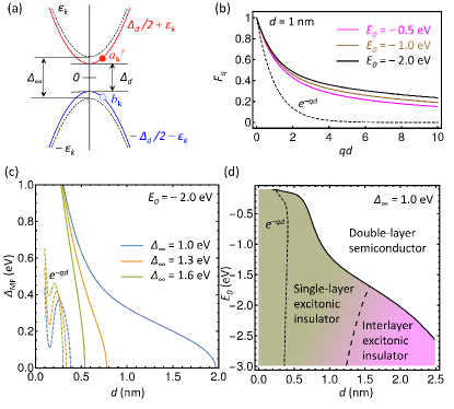
We are now ready to write a mean-field Hamiltonian describing the many-body IEI state. To do that, we reduce the four-band model shown in Fig. 2(e) to a two-band one shown in Fig. 3(a) because is supposed to be always large enough to prevent formation of the intralayer EI. The effective model involves one conduction and one valence band hosting electrons and holes in the single-particle states and , respectively. We symmetrize the bands placing the zero-energy level in the middle of the interlayer bandgap. The mean-field Hamiltonian can be then written as Littlewood et al. (2004)
| (15) |
where () are the electron creation operators in the conduction (valence) band, () are the respective hole creation operators, , and the mean-field parameter reads Littlewood et al. (2004)
| (16) |
Here, is the electron-hole interaction matrix element. Using the Bogolubov transformation
| (17) | |||||
| (18) |
with , we arrive at the canonical form of the mean-field Hamiltonian given by
| (19) |
In the low-temperature limit, the mean-field order parameter reads
| (20) |
Equation (20) is formally equivalent to the gap equation derived in the seminal paper Jérome et al. (1967). However, and both depend on in our case. Finally, we assume that the order parameter does not depend on and represents the mean-field bandgap, , which can be found from the gap equation written as
| (21) |
Evaluation of must take into account the wave function overlap between the single particle states and . The two-particle wave function can be written as an antisymmetric combination of the single-particle states given by
| (22) | |||||
where are the coordinates of particles 1 and 2, and are their in-plane wave vectors. Transition from the state with , to the state with , is described by the following matrix element
| (23) | |||||
where . The integrand in Eq. (23) contains four terms, but we have for low-energy electrons and holes (), and the terms containing spinor products between and become negligible, see Eqs. (6) and (7). The remaining two terms are equal. Neglecting unimportant phase factors we have
| (24) |
where , , and with given by
| (25) |
In the conventional limit of the states localized in the respective layers we can approximate , and . If the wave functions overlap, then differs strongly from , as demonstrated in Fig. 3(b).
Introducing we rewrite the gap equation (21) as
| (26) |
where . Figure 3(c) shows solutions of Eq. (26) for different semiconductor bandgaps, with eV being relevant for 2D WSe2 Chaves et al. (2020). The velocity cm/s is typical for 2D transition metal dichalcogenides Kormányos et al. (2015), and the spacer is assumed to be made of -BN with the relative dielectric permittivity of Laturia et al. (2018). The energy depth is taken to be eV but it could be even deeper up to eV (one-half of the -BN monolayer bandgap) Chaves et al. (2020); Zhao et al. (2020).
Figure 3(c) demonstrates clearly that the wave function overlap in is crucial for creating an IEI state at a reasonable . If the overlap is neglected, then the solutions of Eq. (26) shown in Fig. 3(c) by dashed curves exist only at nm, i.e. the critical is smaller than the monolayer thickness. The local maximum of occurs at the point when . It shifts to even smaller when increases. If the overlap is taken into account, then the critical shifts towards larger values reaching nm for eV, see solid curves in Fig. 3(c).
Figure 3(d) combines the data shown in Figs. 3(c) and 2(g). The lower right corner of the phase diagram is the region where IEI state is expected. In that region, Eq. (26) allows for a solution with respect to , and, at the same time, the interlayer coherence time, , is much longer than the typical exciton life-time in 2D semiconductors. In simple terms, the electrons and holes interact strongly but are well separated. The interlayer EI gradually becomes a single-layer one with decreasing . There is no sharp border between the two states because there is always a non-zero interlayer hopping probability for electrons and holes even though it decays exponentially with increasing . In contrast, the normal and correlated phases are separated by a sharp border, as shown by solid curve in Fig. 3(d), because the order parameter equation (21) either has a solution or not.
IV Discussion
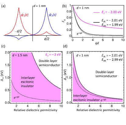
Having established the crucial role of the interlayer coherence in the IEI state we now focus on the effects of the double-layer asymmetry, relative dielectric permittivity of the interlayer media, and the size of a semiconductor bandgap. The double-layer asymmetry influences the IEI state in two different ways. On the one hand, the asymmetry reduces the wave function overlap that results in making the IEI state harder to reach. On the other hand, the asymmetry triggers the collapse of electron and hole wave functions into their respective layers precluding the interlayer coherence effects Santarsiero and Gori (2019) and improving electron-hole separation beneficial for the IEI phase. Note that Eq. (14) estimating makes sense for a symmetric double-layer only.
To quantify the effect of the double-layer asymmetry we introduce , and instead of Eq. (3) we have
| (27) |
The eigenstates of can be still written as with given by
| (28) |
where are the two solutions of the eigenvalue equation given by
| (29) |
In contrast to the symmetric case, Eq. (29) does not allow for an explicit solution but it can be solved numerically Santarsiero and Gori (2019). Figure 4(a) shows the states in a slightly asymmetric double-layer. It is clear that tends to collapse into the left layer whereas does the same into the right one. As and describe, respectively, electron and hole states in our many-body model, the carriers having opposite charges turn out to be well separated in space. Hence, the IEI state should exist even at smaller separations. Figure 4(a) demonstrates, however, that drops significantly even for a slightly asymmetric double-layer and rapidly approaches the form. As a consequence, the many-body gap equation has a solution only at a very small , in the region enclosed by the short-dashed line in Fig. 3(d). Such a small separation does not have physical sense because it is smaller than the monolayer thickness. Hence, an asymmetric double-layer structure made of 2D semiconductors with eV separated by -BN is not suitable for creating the IEI state. A very recent paper Shi et al. (2022), however, offers a way to suppress interlayer tunneling in semiconducting bilayers without dielectric spacer.
There are two obvious options to remedy the situation. First, we could reduce by using a narrow gap 2D semiconductor, such as one of X-enes Chaves et al. (2020); Zheng et al. (2020); Brunetti et al. (2019) or -TiS2 Wei et al. (2017); Singh et al. (2017). Second, we could substitute -BN by a dielectric material with a smaller relative dielectric permittivity, such as silicon dioxide () or polyethylene (). Figures 4(c,d) compare the IEI phase diagrams for the symmetric, Fig. 4(c), and asymmetric, Fig. 4(d), double-layer junctions. The IEI state is supposed to be stable as long as solution of Eq. (26) exists. The interlayer distance is shown in the respective panels. The temperature is assumed to be zero. Note, however, that decreasing semiconductor bandgap might induce transition to the EI state in each layer separately that would make the desired drag-counterflow setup impossible to implement. This transition cannot be described by the simplified two-band many-body model employed in this section.
V Outlook
The results discussed above suggest that the interlayer overlap between electron and hole wave functions potentially facilitates transition into the IEI state. Figure 3(d) is among the main results of the present paper offering a recipe for the IEI state using known 2D materials. The ingredients are one insulating and two semiconducting layers. The semiconducting layers must be identical and possess a direct bandgap of about 1 eV. A much larger bandgap would require either unrealistically strong interaction or unrealistically small interlayer separation to bring the double-layer into the IEI state, whereas a much smaller bandgap would convert each layer into the EI state separately. At the moment, the best choice seems to be 2D TiS3 with the direct bandgap very close to eV taken in Fig. 3(d). The bandgap size has been predicted by means of ab-initio calculations Dai and Zeng (2015) and confirmed experimentally Island et al. (2015). There is strong anisotropy in electronic structure Silva-Guillén et al. (2017) but it is not able to spoil the qualitative applicability of the model proposed. Moreover, 2D TiS3 can be assembled into heterostructures with other 2D materials, Liu et al. (2018) including -BN Papadopoulos et al. (2019) employed in Fig. 3(d) as a spacer. As 2D TiS3 and -BN have similar work functions of about 5 eV, and -BN monolayer has a bandgap of about 6 eV, the resulting band diagram should be similar to that shown in Fig. 2(e) with eV. Having two or three monolayers of -BN as a spacer would bring the electron-hole system into the desired lower-right corner of the phase diagram in Fig. 3(d). The black long-dashed curve separating the single-layer EI from the true IEI state also applies to TiS3, with subpicosecond exciton lifetime Cui et al. (2016). The main obstacle would be to maintain the layer symmetry in the double-junction.
Acknowledgements.
This research is supported by the Ministry of Education, Singapore, under its Research Centre of Excellence award to the Institute for Functional Intelligent Materials (I-FIM, Project No. EDUNC-33-18-279-V12). I am grateful to the Director’s Senior Research Fellowship from the Centre for Advanced 2D Materials at NUS for support as well as thank Giovanni Vignale, Goki Eda, Alexandra Carvalho, and Aleksandr Rodin for discussions.References
- Keldysh and Kopaev (1965) L. V. Keldysh and Y. V. Kopaev, Sov. Phys. Solid State, USSR 6, 2219 (1965).
- Cloizeaux (1965) J. D. Cloizeaux, Journal of Physics and Chemistry of Solids 26, 259 (1965).
- Jérome et al. (1967) D. Jérome, T. Rice, and W. Kohn, Physical Review 158, 462 (1967).
- Bucher et al. (1991) B. Bucher, P. Steiner, and P. Wachter, Phys. Rev. Lett. 67, 2717 (1991).
- Cercellier et al. (2007) H. Cercellier, C. Monney, F. Clerc, C. Battaglia, L. Despont, M. G. Garnier, H. Beck, P. Aebi, L. Patthey, H. Berger, and L. Forró, Phys. Rev. Lett. 99, 146403 (2007).
- Wakisaka et al. (2009) Y. Wakisaka, T. Sudayama, K. Takubo, T. Mizokawa, M. Arita, H. Namatame, M. Taniguchi, N. Katayama, M. Nohara, and H. Takagi, Phys. Rev. Lett. 103, 026402 (2009).
- Lu et al. (2017) Y. F. Lu, H. Kono, T. I. Larkin, A. W. Rost, T. Takayama, A. V. Boris, B. Keimer, and H. Takagi, Nature Commun. 8, 14408 (2017).
- Mor et al. (2017) S. Mor, M. Herzog, D. Golež, P. Werner, M. Eckstein, N. Katayama, M. Nohara, H. Takagi, T. Mizokawa, C. Monney, and J. Stähler, Phys. Rev. Lett. 119, 086401 (2017).
- Wu et al. (2019) X.-J. Wu, W. Lou, K. Chang, G. Sullivan, A. Ikhlassi, and R.-R. Du, Phys. Rev. B 100, 165309 (2019).
- Chui et al. (2021) S. T. Chui, N. Wang, and B. Tanatar, Phys. Rev. B 104, 195432 (2021).
- Sodemann et al. (2012) I. Sodemann, D. A. Pesin, and A. H. MacDonald, Phys. Rev. B 85, 195136 (2012).
- Brunetti et al. (2018) M. N. Brunetti, O. L. Berman, and R. Y. Kezerashvili, Journal of Physics: Condensed Matter 30, 225001 (2018).
- Shi et al. (2022) Q. Shi, E.-M. Shih, D. Rhodes, B. Kim, K. Barmak, K. Watanabe, T. Taniguchi, Z. Papić, D. A. Abanin, J. Hone, et al., Nature Nanotechnology 17, 577 (2022).
- Du et al. (2017) L. Du, X. Li, W. Lou, G. Sullivan, K. Chang, J. Kono, and R.-R. Du, Nature Commun. 8, 1971 (2017).
- Ma et al. (2021) L. Ma, P. X. Nguyen, Z. Wang, Y. Zeng, K. Watanabe, T. Taniguchi, A. H. MacDonald, K. F. Mak, and J. Shan, Nature 598, 585 (2021).
- Zhang et al. (2022) Z. Zhang, E. C. Regan, D. Wang, W. Zhao, S. Wang, M. Sayyad, K. Yumigeta, K. Watanabe, T. Taniguchi, S. Tongay, et al., Nature Physics , not available (2022).
- Su and MacDonald (2008) J.-J. Su and A. MacDonald, Nature Physics 4, 799 (2008).
- Xie and MacDonald (2018) M. Xie and A. H. MacDonald, Phys. Rev. Lett. 121, 067702 (2018).
- Eisenstein and MacDonald (2004) J. Eisenstein and A. MacDonald, Nature 432, 691 (2004).
- Vignale and MacDonald (1996) G. Vignale and A. H. MacDonald, Phys. Rev. Lett. 76, 2786 (1996).
- Trushin (2019) M. Trushin, Phys. Rev. B 99, 205307 (2019).
- Jia et al. (2022) Y. Jia, P. Wang, C.-L. Chiu, Z. Song, G. Yu, B. Jäck, S. Lei, S. Klemenz, F. A. Cevallos, M. Onyszczak, et al., Nature Physics 18, 87 (2022).
- Kohn and Sherrington (1970) W. Kohn and D. Sherrington, Rev. Mod. Phys. 42, 1 (1970).
- Zhu et al. (1995) X. Zhu, P. B. Littlewood, M. S. Hybertsen, and T. M. Rice, Phys. Rev. Lett. 74, 1633 (1995).
- Conti et al. (1998) S. Conti, G. Vignale, and A. H. MacDonald, Phys. Rev. B 57, R6846 (1998).
- Kormányos et al. (2015) A. Kormányos, G. Burkard, M. Gmitra, J. Fabian, V. Zólyomi, N. D. Drummond, and V. Fal’ko, 2D Materials 2, 022001 (2015).
- Xiao et al. (2012) D. Xiao, G.-B. Liu, W. Feng, X. Xu, and W. Yao, Phys. Rev. Lett. 108, 196802 (2012).
- Santarsiero and Gori (2019) M. Santarsiero and F. Gori, European Journal of Physics 40, 055402 (2019).
- Ahmed et al. (2016) Z. Ahmed, S. Kumar, M. Sharma, and V. Sharma, European Journal of Physics 37, 045406 (2016).
- Özcelik et al. (2016) V. O. Özcelik, J. G. Azadani, C. Yang, S. J. Koester, and T. Low, Physical Review B 94, 035125 (2016).
- Wang et al. (2015) H. Wang, C. Zhang, and F. Rana, Nano Letters 15, 339 (2015).
- Yuan and Huang (2015) L. Yuan and L. Huang, Nanoscale 7, 7402 (2015).
- Littlewood et al. (2004) P. B. Littlewood, P. R. Eastham, J. M. J. Keeling, F. M. Marchetti, B. D. Simons, and M. H. Szymanska, Journal of Physics: Condensed Matter 16, S3597 (2004).
- Chaves et al. (2020) A. Chaves, J. Azadani, H. Alsalman, D. Da Costa, R. Frisenda, A. Chaves, S. H. Song, Y. Kim, D. He, J. Zhou, et al., npj 2D Materials and Applications 4, 1 (2020).
- Laturia et al. (2018) A. Laturia, M. L. Van de Put, and W. G. Vandenberghe, npj 2D Materials and Applications 2, 1 (2018).
- Zhao et al. (2020) G. Zhao, J. Wang, Y. Xu, Z. Ma, X. Li, W. Yang, G. Liu, J. Yang, et al., Journal of Alloys and Compounds 834, 155108 (2020).
- Zheng et al. (2020) J. Zheng, Y. Xiang, C. Li, R. Yuan, F. Chi, and Y. Guo, Phys. Rev. Applied 14, 034027 (2020).
- Brunetti et al. (2019) M. N. Brunetti, O. L. Berman, and R. Y. Kezerashvili, Phys. Rev. B 99, 195417 (2019).
- Wei et al. (2017) M. J. Wei, W. J. Lu, R. C. Xiao, H. Y. Lv, P. Tong, W. H. Song, and Y. P. Sun, Phys. Rev. B 96, 165404 (2017).
- Singh et al. (2017) B. Singh, C.-H. Hsu, W.-F. Tsai, V. M. Pereira, and H. Lin, Phys. Rev. B 95, 245136 (2017).
- Dai and Zeng (2015) J. Dai and X. C. Zeng, Angewandte Chemie 127, 7682 (2015).
- Island et al. (2015) J. O. Island, M. Barawi, R. Biele, A. Almazán, J. M. Clamagirand, J. R. Ares, C. Sánchez, H. S. Van Der Zant, J. V. Álvarez, R. D’Agosta, et al., Advanced Materials 27, 2595 (2015).
- Silva-Guillén et al. (2017) J. A. Silva-Guillén, E. Canadell, P. Ordejón, F. Guinea, and R. Roldan, 2D Materials 4, 025085 (2017).
- Liu et al. (2018) J. Liu, Y. Guo, F. Q. Wang, and Q. Wang, Nanoscale 10, 807 (2018).
- Papadopoulos et al. (2019) N. Papadopoulos, E. Flores, K. Watanabe, T. Taniguchi, J. R. Ares, C. Sanchez, I. J. Ferrer, A. Castellanos-Gomez, G. A. Steele, and H. S. Van Der Zant, 2D Materials 7, 015009 (2019).
- Cui et al. (2016) Q. Cui, A. Lipatov, J. S. Wilt, M. Z. Bellus, X. C. Zeng, J. Wu, A. Sinitskii, and H. Zhao, ACS Applied Materials & Interfaces 8, 18334 (2016).