Exciton tuning in monolayer WSe2 via substrate induced electron doping
Abstract
We report on large exciton tuning in WSe2 monolayers via substrate induced non-degenerate doping. We observe a redshift of 62 meV for the exciton together with a 1-2 orders of magnitude photoluminescence (PL) quenching when the monolayer WSe2 is brought in contact with highly oriented pyrolytic graphite (HOPG) compared to the dielectric substrates such as hBN and SiO2. As the evidence of doping from HOPG to WSe2, a drastic increase of the trion emission intensity was observed. Using a systematic PL and Kelvin probe force microscopy (KPFM) investigation on WSe2/HOPG, WSe2/hBN, and WSe2/graphene, we conclude that this unique excitonic behavior is induced by electron doping from the substrate. Our results propose a simple yet efficient way for exciton tuning in monolayer WSe2, which plays a central role in the fundamental understanding and further device development.
1 Introduction
Beyond graphene [1], transition metal dichalcogenides (TMDCs) are currently at the center of 2D materials research, owing to their extraordinary optical, electrical, thermal, mechanical properties [2, 3, 4, 5], and, most importantly, to the unique indirect- to direct-bandgap transition when the material is thinned from bulk to monolayer [6, 7]. Different approaches of exciton tuning and bandgap engineering have been reported such as changing the dielectric environment, mechanical straining, doping, alloying, injecting plasmonic hot electrons, and manipulating the carrier concentration via external electric field [8, 9, 10, 11, 12, 13, 14, 15].
In this work, we report on tuning the exciton energy in monolayer WSe2 via substrate induced non-degenerate electron doping. We observe a 62 meV redshift of the monolayer WSe2 excitonic emission (from 1.65 eV to 1.71 eV) together with a few orders of magnitude photoluminescence (PL) quenching when the material is brought in contact with HOPG compared to the WSe2 excitonic feature on dielectric substrates such as hBN, SiO2, and polydimethylsiloxane (PDMS), which has been measured and reported in our previous work [16]. As a by-product, a drastic increase of the trion emission intensity up to 5.5 times was observed, which is a characteristic of electron doping in TMDC monolayers. To understand this unique behavior, we employed a systematic PL and Kelvin probe force microscopy (KPFM) investigation on different TMDC/substrate combinations, namely WSe2/HOPG, WSe2/graphene, and WSe2/hBN as a reference. Surprisingly, we were only able to observe such pronounced redshift when WSe2 is in contact with HOPG but not with graphene. The KPFM measurements provide different contact potential difference (CPD) values when comparing WSe2/HOPG to WSe2/graphene and WSe2/hBN. This indicates different Fermi level positions and different carrier concentrations in WSe2. The PL quenching, redshift, increase of trion emission intensity, and different CPD values all conclusively point towards electrons from the HOPG substrate injected to WSe2 and leading to bandgap renormalization and thus the tuning of exciton energy. Our work explains the unique behavior of monolayer WSe2/HOPG and demonstrates a simple yet efficient method, which enables to tune the exciton energy in monolayer WSe2 by 62 meV. This is essential for fundamental studies and the development of devices such as photodetectors, excitonic LEDs, and the coupling with plasmonics [17, 18, 19, 20].
2 Materials and methods
2.1 Sample preparation
Few layer hBN (from 2D semiconductors), graphene (from NGS Naturgraphit), and monolayer WSe2 (from HQ graphene) are mechanically exfoliated from their bulk crystals via Nitto tape onto a PDMS stamp and then transferred bottom-to-top onto the HOPG substrate following a deterministic all-dry transfer technique [21, 22]. All materials on PDMS are first characterized by PL and Raman prior to transfer. HOPG was cleaved before transfer to ensure a fresh surface. After transfer, the samples are annealed in a nitrogen atmosphere at 150 °C for 2 hours to optimize the contact between flakes and ensure a clean surface. The detailed process used for sample fabrication is shown in Figs. 1S and 2S.
2.2 Optical spectroscopy
PL measurements are performed using a Horiba Xplora Plus equipped with a 100x, 0.9 NA objective, a spectrometer comprising 600 l/mm grating, and an electron-multiplying CCD (EMCCD). A DPSS 532 nm CW laser source was used for excitation. The laser power is 100 µW measured under the objective for PL measurements if not specified differently. The setup is equipped with a Märzhäuser motorized stage with a 100 nm step size precision for PL mapping.
Raman spectra are acquired by a Horiba LabRAM HR spectrometer with a 100x, 0.9 NA objective, 2400 l/mm grating, and a liquid nitrogen cooled Symphony CCD detector. A solid-state 514.7 nm laser is used for excitation with a laser power 100 µW measured under the objective. We choose a confocal pinhole of 50 µm to reach a high spectral resolution of approximately .
2.3 Kelvin probe force microscope
We use an AIST-NT SmartSPMTM 1000 for KPFM measurements. The KPFM measurements are performed in ambient condition with constant temperature and humidity. The NSG10 Pt coated tip is commercially available with a typical tip radius of 35 nm.
3 Results and discussion
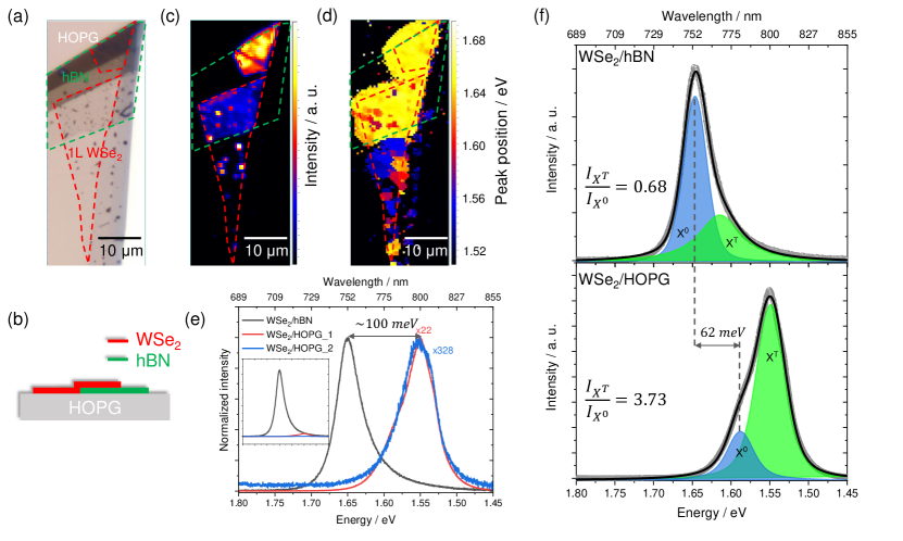
Figs. 1(a) and (b) display the optical microscope image and the schematic cross section of a WSe2/hBN/HOPG hetero-stack, respectively. The monolayer WSe2 is transferred onto the hBN/HOPG hetero-stack in a way that it creates contacts with both few layer hBN and HOPG. According to the atomic force microscopy (AFM) measurement shown in Fig. 4S, the top brown-colored hBN has a thickness of 38.2 nm, and the middle part has a thickness of 3.8 nm. We acquired a micro PL map on the sample with a step size of 0.5 µm. As shown in the intensity map in Fig. 1(c), the PL intensity of WSe2 on thick hBN is higher than that on thin hBN because of interference enhancement [23, 24]. More importantly, comparing the PL intensity of WSe2 on hBN and HOPG, one can clearly identify that a drastic decrease of PL intensity occurs on HOPG. The few dots that still remain intense may correspond to bubbles or hydrocarbon contaminations at the interface, which can enhance the PL signal [25, 26, 27]. Fig. 1(d) displays the peak position map indicating that the sample is clearly divided into two parts: WSe2/hBN with a peak position of 1.65 eV and WSe2/HOPG with a peak position of 1.55 eV.
The detailed spectra of WSe2/hBN and WSe2/HOPG are shown in Fig. 1(e). A strong PL quenching of 1-2 orders of magnitude is observed when WSe2 is in contact with HOPG, which indicates charge dissociation through the junction or charge transfer between WSe2 and HOPG [24, 28]. Monolayer WSe2 on hBN shows a characteristic PL at 1.65 eV, which is consistent with the literature values [16, 29], while the PL peak position of WSe2/HOPG shows a marked 100 meV redshift, which is much higher than the reported value caused by changing of dielectric environment [8]. Besides the quenching and redshift, the PL line shape changes significantly. We thus decomposed the PL spectra into peaks corresponding to the radiative recombination of different exciton/trion species in monolayer WSe2. As shown in Fig. 1(f), two peaks with a Voigt line shape were identified in the fitted spectra. The neutral exciton () originates from the direct bandgap transition at the point in the Brillouin zone and there is a charged exciton peak also known as trion [29, 30, 31, 32]. We also investigated the Stokes shift of monolayer WSe2 as shown in Fig. 3S, which is negligible with value of 2 meV. It is therefore fair enough to consider the PL peak position as the exciton energy. The fitting result suggests a 62 meV redshift of and most interestingly, a drastic increase of the relative intensity. The ratio of increases from 0.68 on hBN to 3.73 on HOPG, which is a strong evidence of higher electron concentration in WSe2 on HOPG than in WSe2 on hBN.
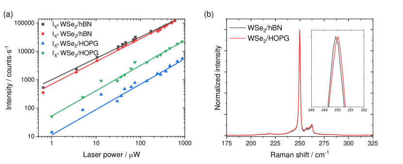
Even though we propose that charge transfer and electron doping from HOPG to monolayer WSe2 seem to be the most reasonable mechanism of PL quenching, redshift, and increasing trion emission intensity, we still carefully examined that they do not originate from the defect-bound localized states or strain due to lattice mismatch. Power dependent PL intensities of WSe2/hBN and WSe2/HOPG are displayed in Fig. 2(a). The PL intensity is obtained from the integrated area of the Voigt fitted and features. The PL intensity as a function of excitation laser power is then fitted by a power law: [29, 33], where the extracted exponential factor , , , and for and on WSe2/hBN and WSe2/HOPG, respectively. The fitting results suggest a sublinear power dependence of the PL intensity for both and on WSe2/hBN and WSe2/HOPG and do not show any saturation phenomena at high laser power, which excludes the possibility of defects as the origin of the observed behavior [34]. Fig. 2(b) shows the high spectral resolution (0.8 ) Raman spectra of WSe2/hBN and WSe2/HOPG. The most intense peak at 250 corresponds to the combination of the in-plane and out-of-plane vibrational modes, which are almost degenerate at the same frequency [16, 35, 36, 37]. The feature at 260 is a second order peak caused by a double resonance effect involving the longitudinal acoustic phonon at the point in the Brillouin zone assigned as 2LA(M) [37, 38]. The mode is highly sensitive to the strain [39, 40]. The fitted Raman spectra reveal a small 0.15 peak position difference, which indicates that strain is also small and cannot account for the huge redshift in PL.
KPFM is a powerful technique to obtain local surface potential and Fermi level position in the nanoscale [24, 41]. We therefore measured KPFM on the WSe2/hBN/HOPG hetero-stack to obtain further insight in the energy level alignment at the various interfaces. In the ideal case KPFM measures the contact potential difference (CPD) between the metallic AFM tip and the sample according to the relation: , where and are the work functions of the sample and the tip, and is the elementary charge. KPFM does not give a quantitative, absolute value of the Fermi level position in ambient conditions, because the CPD value is known to be strongly influenced by the measurement environment, tip geometry, parasitic effects such as capacitive coupling, as well as the chosen experimental parameters [42, 43, 44, 45]. Nevertheless, it still qualitatively indicates the trend of Fermi level position and material work functions [24, 41, 46, 47]. The values of the energy levels discussed in the following paragraph are directly extracted from the KPFM measurements.
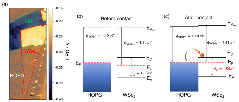
Fig. 3(a) shows the CPD map of WSe2/hBN/HOPG. Even though it is the same monolayer WSe2 flake, one can clearly distinguish the high contrast between WSe2 on hBN and WSe2 on HOPG. The absolute work function of HOPG is determine to be by an ultraviolet photoelectron spectroscopy (UPS) measurement shown in Fig. 6S. The electron affinity of monolayer WSe2 is reported to be 3.7-3.9 eV [48, 49]. We therefore calculate and draw the band diagrams of WSe2 before (on hBN) and after (on HOPG) contacting with HOPG in Figs. 3(b) and (c), respectively. The band diagrams reveal a decrease of the work function or increase of Fermi level when WSe2 is in contact with HOPG, which indicates higher electron concentration in WSe2 on HOPG than in WSe2 on hBN. The high electron concentration in WSe2/HOPG can only originate from electron doping from HOPG to WSe2, which explains the PL quenching, redshift, and increasing trion emission intensity shown in Fig. 1.
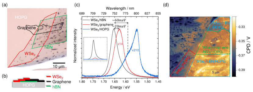
Apparently interfacing WSe2 with HOPG results in an efficient tuning of the exciton emission in a straightforward manner. Researchers also studied the combination of WSe2 and graphene [8], yet did not report similar results. This naturally leads to the question: do graphene and graphite lead to a different interaction when interfaced with WSe2? To answer this question, we prepared a hetero-stack of WSe2/graphene/hBN/HOPG as shown in Figs. 4(a) and (b), where WSe2 is partially on hBN, partially on graphene, and partially on HOPG. The PL spectra of WSe2/hBN, WSe2/graphene, and WSe2/HOPG are shown in Fig. 4(c). Again, we observe similar PL quenching, redshift, and increasing trion emission intensity for WSe2 on HOPG. However, a redshift of only 20 meV is detected on WSe2/graphene, which is in excellent agreement with the value reported by Raja et al. [8]. This redshift of the exciton is attributed to the altered local dielectric screening of the Coulomb interaction in WSe2. A higher trion emission intensity is also not observed in the case of WSe2/graphene. This clearly indicates that the interaction for WSe2 on graphene is different from that for WSe2 on HOPG. We assume that this difference is due to the lower amount of free electrons in graphene than that in HOPG. The KPFM measurement performed on such a sample is displayed in Fig. 4(d). A CPD contrast is only observed between WSe2/HOPG and WSe2/hBN with a value of , while WSe2/graphene and WSe2/hBN reveal a negligible difference of . This suggests that a significant change of the Fermi level position occurs due to electron doping from the substrate and only happens for WSe2 on HOPG but not for WSe2 on graphene.
4 Conclusions
In summary, we investigated WSe2/hBN, WSe2/graphene, and WSe2/HOPG hetero-stacks. We observed a strong PL intensity quenching, 62 meV redshift of the exciton, and a drastic increase of the trion emission intensity on WSe2/HOPG compared to WSe2/graphene and WSe2/hBN. The KPFM results reveal a high CPD contrast, which indicates a renormalization of the energy level alignment at the interface. The effects observed for WSe2 on HOPG are thus assigned to significant electron doping of the WSe2 monolayer from the HOPG substrate. We propose a simple yet efficient way to tune the exciton emission in monolayer WSe2 by substrate induced electron doping.
5 Acknowledgments
The authors gratefully acknowledge financial support by the Deutsche Forschungsgemeinschaft (DFG, projects ZA 146/43-1 and ZA 146/47-1). M.A.A. and A.M. acknowledge financial support by the Austrian Science Fund (FWF) under the grant no. I4323-N36. We thank Manuel Monecke for helping the UPS measurement.
6 Author contributions
Y.P. fabricated the samples, performed the measurements and analyzed the data. M.R., I.M. L.H., and T.I.M. contributed to data analysis and discussion. G.M., T.B. and A.W. performed the reflectance contrast measurement. M.A.A. and A.M. provided the graphene. D.R.T.Z. supervised the work. M.R. and D.R.T.Z. were involved in the evaluation and interpretation of the results. Y.P. wrote the manuscript. All authors discussed the results and commented on the manuscript.
7 Conflict of interest
The authors declare no conflict of interest.
References
- [1] Kostya S Novoselov et al. “Electric field effect in atomically thin carbon films” In science 306.5696 American Association for the Advancement of Science, 2004, pp. 666–669
- [2] Jl A Wilson and AD Yoffe “The transition metal dichalcogenides discussion and interpretation of the observed optical, electrical and structural properties” In Advances in Physics 18.73 Taylor & Francis, 1969, pp. 193–335
- [3] Sanfeng Wu et al. “Vapor–solid growth of high optical quality MoS2 monolayers with near-unity valley polarization” In ACS nano 7.3 ACS Publications, 2013, pp. 2768–2772
- [4] Namphung Peimyoo et al. “Thermal conductivity determination of suspended mono-and bilayer WS2 by Raman spectroscopy” In Nano Research 8.4 Springer, 2015, pp. 1210–1221
- [5] Yuanzheng Li et al. “Enhancement of exciton emission from multilayer MoS2 at high temperatures: intervalley transfer versus interlayer decoupling” In Small 13.17 Wiley Online Library, 2017, pp. 1700157
- [6] Andrea Splendiani et al. “Emerging photoluminescence in monolayer MoS2” In Nano letters 10.4 ACS Publications, 2010, pp. 1271–1275
- [7] Yuanzheng Li et al. “Accurate identification of layer number for few-layer WS2 and WSe2 via spectroscopic study” In Nanotechnology 29.12 IOP Publishing, 2018, pp. 124001
- [8] Archana Raja et al. “Coulomb engineering of the bandgap and excitons in two-dimensional materials” In Nature communications 8.1 Nature Publishing Group, 2017, pp. 1–7
- [9] Yongji Gong et al. “Band gap engineering and layer-by-layer mapping of selenium-doped molybdenum disulfide” In Nano letters 14.2 ACS Publications, 2014, pp. 442–449
- [10] Hiram J Conley et al. “Bandgap engineering of strained monolayer and bilayer MoS2” In Nano letters 13.8 ACS Publications, 2013, pp. 3626–3630
- [11] Riccardo Frisenda et al. “Biaxial strain tuning of the optical properties of single-layer transition metal dichalcogenides” In npj 2D Materials and Applications 1.1 Nature Publishing Group, 2017, pp. 1–7
- [12] Ziwei Li et al. “Active light control of the MoS2 monolayer exciton binding energy” In ACS nano 9.10 ACS Publications, 2015, pp. 10158–10164
- [13] Paul V Nguyen et al. “Visualizing electrostatic gating effects in two-dimensional heterostructures” In Nature 572.7768 Nature Publishing Group, 2019, pp. 220–223
- [14] Luis Fernández et al. “Renormalization of the band gap in 2D materials through the competition between electromagnetic and four-fermion interactions in large N expansion” In Physical Review D 102.1 APS, 2020, pp. 016020
- [15] A Chaves et al. “Bandgap engineering of two-dimensional semiconductor materials” In npj 2D Materials and Applications 4.1 Nature Publishing Group, 2020, pp. 1–21
- [16] Philipp Tonndorf et al. “Photoluminescence emission and Raman response of monolayer MoS2, MoSe2, and WSe2” In Optics express 21.4 Optical Society of America, 2013, pp. 4908–4916
- [17] Changjian Zhou et al. “Self-driven WSe2 photodetectors enabled with asymmetrical van der Waals contact interfaces” In npj 2D Materials and Applications 4.1 Nature Publishing Group, 2020, pp. 1–9
- [18] Jun Xiao, Mervin Zhao, Yuan Wang and Xiang Zhang “Excitons in atomically thin 2D semiconductors and their applications” In Nanophotonics 6.6 De Gruyter, 2017, pp. 1309–1328
- [19] Wenjing Liu et al. “Strong exciton–plasmon coupling in MoS2 coupled with plasmonic lattice” In Nano letters 16.2 ACS Publications, 2016, pp. 1262–1269
- [20] Jason S Ross et al. “Electrically tunable excitonic light-emitting diodes based on monolayer WSe2 p–n junctions” In Nature nanotechnology 9.4 Nature Publishing Group, 2014, pp. 268–272
- [21] Andres Castellanos-Gomez et al. “Deterministic transfer of two-dimensional materials by all-dry viscoelastic stamping” In 2D Materials 1.1 IOP Publishing, 2014, pp. 011002
- [22] Jens Kunstmann et al. “Momentum-space indirect interlayer excitons in transition-metal dichalcogenide van der Waals heterostructures” In Nature Physics 14.8 Nature Publishing Group, 2018, pp. 801–805
- [23] Li Ding et al. “Understanding interlayer coupling in TMD-HBN heterostructure by Raman spectroscopy” In IEEE Transactions on Electron Devices 65.10 IEEE, 2018, pp. 4059–4067
- [24] Rafael R Rojas-Lopez et al. “Photoluminescence and charge transfer in the prototypical 2D/3D semiconductor heterostructure MoS2/GaAs” In Applied Physics Letters 119.23 AIP Publishing LLC, 2021, pp. 233101
- [25] DG Purdie et al. “Cleaning interfaces in layered materials heterostructures” In Nature communications 9.1 Nature Publishing Group, 2018, pp. 1–12
- [26] Sarah J Haigh et al. “Cross-sectional imaging of individual layers and buried interfaces of graphene-based heterostructures and superlattices” In Nature materials 11.9 Nature Publishing Group, 2012, pp. 764–767
- [27] Anastasia V Tyurnina et al. “Strained bubbles in van der Waals heterostructures as local emitters of photoluminescence with adjustable wavelength” In ACS photonics 6.2 ACS Publications, 2019, pp. 516–524
- [28] Yunjeong Hwang, Taehun Kim and Naechul Shin “Interlayer Energy Transfer and Photoluminescence Quenching in MoSe2/Graphene van der Waals Heterostructures for Optoelectronic Devices” In ACS Applied Nano Materials 4.11 ACS Publications, 2021, pp. 12034–12042
- [29] Jiani Huang, Thang B Hoang and Maiken H Mikkelsen “Probing the origin of excitonic states in monolayer WSe2” In Scientific reports 6.1 Nature Publishing Group, 2016, pp. 1–7
- [30] Erfu Liu et al. “Valley-selective chiral phonon replicas of dark excitons and trions in monolayer WSe2” In Physical Review Research 1.3 APS, 2019, pp. 032007
- [31] Minhao He et al. “Valley phonons and exciton complexes in a monolayer semiconductor” In Nature communications 11.1 Nature Publishing Group, 2020, pp. 1–7
- [32] Zhipeng Li et al. “Fine structures of valley-polarized excitonic states in monolayer transitional metal dichalcogenides” In Nanophotonics 9.7 De Gruyter, 2020, pp. 1811–1829
- [33] Zhangting Wu et al. “Defects as a factor limiting carrier mobility in WSe2: A spectroscopic investigation” In Nano Research 9.12 Springer, 2016, pp. 3622–3631
- [34] Zhangting Wu and Zhenhua Ni “Spectroscopic investigation of defects in two-dimensional materials” In Nanophotonics 6.6 De Gruyter, 2017, pp. 1219–1237
- [35] Xin Luo et al. “Effects of lower symmetry and dimensionality on Raman spectra in two-dimensional WSe2” In Physical Review B 88.19 APS, 2013, pp. 195313
- [36] Weijie Zhao et al. “Lattice dynamics in mono-and few-layer sheets of WS2 and WSe2” In Nanoscale 5.20 Royal Society of Chemistry, 2013, pp. 9677–9683
- [37] H Terrones et al. “New first order Raman-active modes in few layered transition metal dichalcogenides” In Scientific reports 4.1 Nature Publishing Group, 2014, pp. 1–9
- [38] Elena Del Corro et al. “Excited excitonic states in 1L, 2L, 3L, and bulk WSe2 observed by resonant Raman spectroscopy” In Acs Nano 8.9 ACS Publications, 2014, pp. 9629–9635
- [39] AM Dadgar et al. “Strain engineering and Raman spectroscopy of monolayer transition metal dichalcogenides” In Chemistry of Materials 30.15 ACS Publications, 2018, pp. 5148–5155
- [40] Sujay B Desai et al. “Strain-induced indirect to direct bandgap transition in multilayer WSe2” In Nano letters 14.8 ACS Publications, 2014, pp. 4592–4597
- [41] Wilhelm Melitz, Jian Shen, Andrew C Kummel and Sangyeob Lee “Kelvin probe force microscopy and its application” In Surface science reports 66.1 Elsevier, 2011, pp. 1–27
- [42] Cristina E Giusca et al. “Water affinity to epitaxial graphene: the impact of layer thickness” In Advanced Materials Interfaces 2.16 Wiley Online Library, 2015, pp. 1500252
- [43] HO Jacobs, Pascal Leuchtmann, OJ Homan and A Stemmer “Resolution and contrast in Kelvin probe force microscopy” In Journal of applied physics 84.3 American Institute of Physics, 1998, pp. 1168–1173
- [44] Sophie Barbet et al. “Cross-talk artefacts in Kelvin probe force microscopy imaging: a comprehensive study” In Journal of Applied Physics 115.14 American Institute of Physics, 2014, pp. 144313
- [45] HO Jacobs, HF Knapp and AROSI Stemmer “Practical aspects of Kelvin probe force microscopy” In Review of scientific instruments 70.3 American Institute of Physics, 1999, pp. 1756–1760
- [46] Elisa G Castanon et al. “Calibrated Kelvin-probe force microscopy of 2D materials using Pt-coated probes” In Journal of Physics Communications 4.9 IOP Publishing, 2020, pp. 095025
- [47] Aleksandar Matković et al. “Interfacial band engineering of MoS2/gold interfaces using pyrimidine-containing self-assembled monolayers: toward contact-resistance-free bottom-contacts” In Advanced Electronic Materials 6.5 Wiley Online Library, 2020, pp. 2000110
- [48] Jingwei Xiao et al. “Enhanced performance of a monolayer MoS2/WSe2 heterojunction as a photoelectrochemical cathode” In Nano-Micro Letters 10.4 Springer, 2018, pp. 1–9
- [49] Wei Liu, W Cao, Jiahao Kang and Kaustav Banerjee “High-performance field-effect-transistors on monolayer-WSe2” In ECS Transactions 58.7 IOP Publishing, 2013, pp. 281
See pages 1,2,3,4,5,6 of Exciton_tuning_in_monolayer_WSe2_via_substrate_induced_electron_doping_SI.pdf