InAs-Al Hybrid Devices Passing the Topological Gap Protocol
Abstract
We present measurements and simulations of semiconductor-superconductor heterostructure devices that are consistent with the observation of topological superconductivity and Majorana zero modes. The devices are fabricated from high-mobility two-dimensional electron gases in which quasi-one-dimensional wires are defined by electrostatic gates. These devices enable measurements of local and non-local transport properties and have been optimized via extensive simulations to ensure robustness against non-uniformity and disorder. Our main result is that several devices, fabricated according to the design’s engineering specifications, have passed the topological gap protocol defined in Pikulin et al. [arXiv:2103.12217]. This protocol is a stringent test composed of a sequence of three-terminal local and non-local transport measurements performed while varying the magnetic field, semiconductor electron density, and junction transparencies. Passing the protocol indicates a high probability of detection of a topological phase hosting Majorana zero modes as determined by large-scale disorder simulations. Our experimental results are consistent with a quantum phase transition into a topological superconducting phase that extends over several hundred millitesla in magnetic field and several millivolts in gate voltage, corresponding to approximately one hundred micro-electron-volts in Zeeman energy and chemical potential in the semiconducting wire. These regions feature a closing and re-opening of the bulk gap, with simultaneous zero-bias conductance peaks at both ends of the devices that withstand changes in the junction transparencies. The extracted maximum topological gaps in our devices are 20-. This demonstration is a prerequisite for experiments involving fusion and braiding of Majorana zero modes.
1 Introduction
Topological quantum computation offers the promise of a high degree of intrinsic hardware-level fault-tolerance [1, 2, 3, 4, 5, 6], potentially enabling a single-module quantum computing system that is capable of solving critical problems sufficiently rapidly to have societal impact [7]. This approach hinges on (a) reliably producing a stable topological phase of matter that supports non-Abelian quasiparticles or defects and (b) processing quantum information through protected operations, such as braiding. The former is challenging due to the material parameter and disorder requirements for topological phases of matter. In this paper, we report on three-terminal semiconductor-superconductor nanowire devices that pass the stringent topological gap protocol [8] and therefore satisfy these requirements. We further extract the gap associated with the topological superconducting phase in our devices [9, 10, 11, 12].
Topological phases are a form of matter in which the ground state has long-range quantum entanglement and there is a gap to excited states [13]. Unlike phases of matter that can be distinguished completely by local measurements, topological phases are identified by the transformations of their low-energy states that result from fusing and braiding their quasiparticles and defects. Directly measuring these properties in experiments is rather subtle [14], hindering efforts to fully determine the topological order of candidate materials. In the fractional quantum Hall regime, for example, a quantized Hall conductance reveals the presence of a non-trivial topological phase, but many different topological phases can have the same Hall conductance. Consequently, different measurements are necessary to determine which topological phase is present in a given device [15, 16, 17, 18, 19, 20, 21, 22].
In the case of quasi-one-dimensional superconducting wires without any symmetries enforced, there are only two phases — one trivial and one topological. The latter supports Majorana zero modes (MZMs) localized at the ends of the nanowire [9, 11, 12]. While MZMs can be directly detected through fusion and braiding, one of their auxiliary signatures are zero-bias peaks (ZBPs) in the differential tunneling conductance at the nanowire’s ends [23, 24, 25, 26, 27, 28]. Indeed, most of the earlier experimental studies of candidate topological superconductors focused on ZBPs [29, 30, 31, 32, 33, 34, 35, 36, 37, 38, 39, 40, 41, 42]. However, ZBPs can also be caused by disorder [43, 44, 45], smooth potential variations near the tunnel junction [46, 47, 48, 49, 50, 51], unintentional quantum dots [52, 53], or a supercurrent [54]. These trivial ZBPs can persist over a fairly large range of system parameters [55, 56, 57].
A ZBP associated with an MZM must have a partner at the other end of the wire and should be stable to variations in the electric and magnetic fields in the device. The stability of MZMs with respect to such variations is determined by the bulk gap. However, if a device has a sufficiently large number of control parameters, it is likely that it can be tuned into a configuration in which it has trivial ZBPs at both ends. Meanwhile, the predicted range of stability of a topological phase depends strongly on device geometry, the full stack of materials, and disorder, rendering it difficult to distinguish “stable” ZBPs from “accidental” ones purely empirically. Analyzing the detailed shapes of tunneling conductance spectra leads to some loose qualitative patterns, but there is no sharp binary distinction between the local tunneling conductance spectra associated with MZMs and trivial ZBPs at non-zero temperature. In short, neither more extensive data sets of ZBPs nor more beautiful ZBPs can distinguish the topological and trivial phases. Therefore, it is crucial to develop a practical, reliable protocol that enables the detection of the topological superconducting phase of a nanowire, and it is clear that additional measurements beyond the tunneling conductance are necessary for such a protocol.
This challenge is addressed by the topological gap protocol (TGP) [8], which is designed to reliably identify the topological phase through a series of stringent experimental tests. At the heart of this protocol is the fact that there is necessarily a quantum phase transition between the trivial and topological phases [58]. The protocol detects a bulk phase transition between low-magnetic-field and high-magnetic-field phases via a bulk gap closing. It establishes that the high-field phase is topological through the stability of its ZBPs, in a manner that we specify below. The TGP requires three-terminal device geometries, which overcome the limitations of many earlier two-terminal devices. They allow ZBPs to be simultaneously observed at both ends and also allow for a measurement of the bulk transport gap through the non-local conductance. The protocol is passed when (a) ZBPs are observed in the local conductances measured at tunnel junctions at both ends of a wire, and they are stable to changes in the junction transparency; (b) these stable ZBPs persist over a range of magnetic fields and electron densities in the wire; (c) a closing and re-opening of the bulk transport gap is detected in the non-local conductances; (d) there is a region in the bulk phase diagram whose boundary is gapless and whose interior is gapped and has stable ZBPs; (e) the observed bulk transport gap throughout this region — the topological gap — exceeds the resolution of the measurement.
The hallmarks of most topological phases, including the one discussed here, are rather subtle: there is no signature as immediate as a quantized conductance or Meissner effect. Instead, the existence of a topological phase is imprinted on the measurable properties of the system in a manner that can only be identified through an elaborate measurement and analysis procedure such as the TGP or the even more elaborate procedures necessary for fusion and braiding. Thus, it is of paramount importance that the TGP has been validated by applying it to simulated transport data, especially since the tunneling spectroscopy and transport measurements comprising the TGP do not measure a topological invariant directly.
In simulated devices, we know whether there is a topological phase since we can compute a topological invariant. Hence, we tested the TGP on transport data from simulated devices by comparing its output to this topological invariant. We emphasize that we have not attempted to establish qualitative similarities between simulated and measured conductance plots and this is not the purpose of these simulations. The goal is see if the TGP correctly distinguishes between regions with trivial and non-trivial topological invariant.
We simulated hundreds of devices with different disorder levels and concluded that if a device passes the TGP, then the probability that the candidate region in the phase diagram is not topological is at the 95% confidence level. The TGP thereby distinguishes MZMs from trivial Andreev bound states and determines whether topological superconductivity is present in the parameter range scanned in a data set. Having thus confirmed the reliability of the TGP on simulated data, we formulate the central question of this paper: can we fabricate and measure devices that pass the TGP?
We answer this question in the affirmative by presenting data from four devices, named A, B, C, and D, that have passed this protocol with respective maximum topological gaps ranging between 20-. As we explain in more detail in Sec. 2, our devices are based on heterostructures combining indium arsenide (InAs) and aluminum (Al). The superconducting component is an Al strip, epitaxially-grown on the semiconductor so that it induces superconductivity via the proximity effect. The semiconducting portion is a shallow InAs quantum well hosting a two-dimensional electron gas (2DEG) that has been depleted by electrostatic gates, except for a narrow conducting wire that remains underneath the aluminum strip. Within this suite of components, we have used simulations to optimize the material stack and the device geometry with respect to the topological gap.
Disorder is the principal obstacle to realizing a topological phase supporting MZMs. We have used simulations to predict the (design-dependent) disorder level that the topological phase can tolerate. These simulations incorporate self-consistent electrostatics, the orbital effect of the magnetic field, and realistic semiconductor-superconductor coupling; see Refs. [59, 60, 41] for more details. Consequently, they show both qualitatively and quantitatively how device design can impact the effective disorder strength. Many of the resulting specifications are quite demanding, including: (1) higher mobility () than previously achieved in shallow InAs quantum wells and (2) gate-defined wires that are sufficiently narrow (nm) as to enable tuning into the single sub-band regime.
Our simulations indicate that mesoscopic fluctuations are important. Even devices with the same average disorder level can have different TGP outcomes: some disorder realizations will pass while others fail. The disorder strength determines an expected yield for passing the TGP which is between 0% and 100% over a range of disorder levels. As expected from these simulation results, we have also measured devices that were similar to devices A-D but did not pass the TGP, and we report on data from two of them, which have been named devices E and F.
In summary, each of devices A-D has a high probability of being in the topological phase. To the best of our knowledge, these devices are the first to have passed as stringent a set of requirements as those encompassed by the TGP, namely (a) concurrent ZBPs that are stable both with respect to changes of the junction parameters and also with respect to changes of the bulk parameters that are larger (in appropriate units) than the bulk gap; and (b) a bulk gap closing and re-opening in response to an increasing magnetic field that is visible in the non-local conductance, indicating a quantum phase transition into a phase with correlated ZBPs.
2 Topological gap device design and requirements
2.1 Proximitized semiconductor nanowire model and its topological phase diagram
In this section we briefly review the proximitized nanowire model [11, 12] which supports topological superconductivity over a range of densities and magnetic fields. The minimal model is comprised of a semiconductor nanowire with Rashba spin-orbit interaction coupled to a conventional (-wave) superconductor. The effective Hamiltonian for such a system is:
| (1) | |||
Here, “SM” and “SC” are abbreviations for, respectively, semiconductor and superconductor, , and are the effective mass, chemical potential, and Rashba spin-orbit coupling, respectively. is the Zeeman splitting due to the applied magnetic field along the nanowire: , where and are, respectively, the Landé -factor and Bohr magneton. The proximity to the -wave superconductor is effectively described by the pairing operator , while is the induced pairing potential.
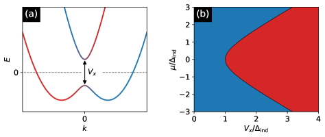
The zero-temperature phase diagram of the proximitized nanowire Hamiltonian of Eq. 1 consists of a trivial (-wave-like) phase and a topological phase, as shown in Fig. 1. The latter supports MZMs at the opposite ends of the nanowire and is in the same phase as a spinless -wave superconductor [9]. The trivial and topological phases are separated by a quantum phase transition at which is necessarily accompanied by the closing of the bulk gap. The stability of a topological phase is characterized by its bulk transport gap or, equivalently, the gap to extended excited states, which we call the topological gap . In the idealized case of Eq. 1, this is simply the bulk gap. This phase has been proposed to occur in quasi-one-dimensional systems composed of chains of magnetic atoms on the surface of a superconductor [61, 62, 63, 64, 65] and in nanowires that are completely encircled by a superconducting shell in which the order parameter winds around the wire due to the orbital effect of the magnetic field [66, 67, 41]. The corresponding two-dimensional topological superconducting state can occur in superconductors [58], at the surface of a topological insulator [68, 69, 70], in ferromagnetic insulator-semiconductor-superconductor heterostructures [10, 71, 72, 73, 74, 75, 38], and in -wave superfluids of ultra-cold fermionic atoms [76, 77].
The model discussed so far neglects many of the ingredients of real devices, such as additional sub-bands and the orbital effect of the magnetic field. To address this, we have developed realistic 3D simulations that take these effects into account. These simulations include self-consistent electrostatics, orbital magnetic field contributions, and realistic semiconductor-superconductor coupling [78, 79, 80, 60, 59, 81]. We have validated these simulations through comparison with ARPES [82], THz spectroscopy [83], the Hall bar measurements reported in Appendix B, and transport through multiple types of previous devices involving proximitized semiconductor nanowires [84, 41, 85, 86]. We also take into account multiple disorder mechanisms such as charged disorder and variations of geometry and composition along the wire length, as discussed in Sec. 2.5. The superconductor’s degrees of freedom are integrated out, yielding a formulation in which it is encapsulated by self-energy boundary conditions [41, 85, 86]. Using this advanced simulation model, we optimized the design for gate-defined devices based on high-quality 2DEG heterostructures in order to minimize the effects of disorder, additional sub-bands, and the orbital effect of the magnetic field. This design is presented in the next subsection. In addition to performing transport simulations with this full model, we extract the parameters of a minimal model projected to the lowest sub-band in Sec. A.1. The parameters that define this effective single sub-band model are listed in Sec. 2.4. After we have discussed the device design, we describe the general effects of disorder in mesoscopic topological wires, then quantify the effective disorder potential in our devices.
2.2 Gate-defined proximitized nanowire
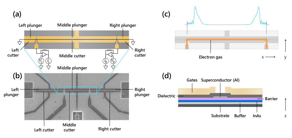
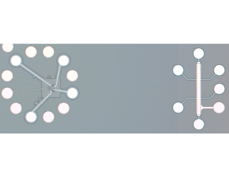
Our devices are defined by an Al strip separated from an InAs quantum well by a barrier layer. There are two designs which are conceptually similar but have some practical differences. One has a single-layer gate (SLG) design while the other has a dual-layer gate (DLG) design, shown in Fig. 2 and Fig. 3, respectively. We will refer to both designs as “topological gap devices.” A cross-section of an SLG device is shown in Fig. 2(d), where the Al strip is light grey. The strip’s dimensions have been optimized using the simulations described above: length , width nm, thickness nm.
The length is in the direction perpendicular to the cross-section in Fig. 2(d). The Al strip is covered by a several nm thick top oxide formed by controlled oxidation [not shown in Fig. 2(d) or Fig. 3(c)]. The Al strip features larger Al pads at each end of its length, which can be seen at the right and left edges of the scanning electron micrograph (SEM) images in Fig. 2(b) and Fig. 3(b). The pads are contacted with Ti/Au or Ti/Al Ohmic leads, by which the Al strip is grounded. (Both types of contacts are normal in the typical operating regime.) We will denote the direction perpendicular to the surface of the quantum well as the -direction, while the directions along and perpendicular to the Al strip are the - and -direction, respectively, as shown in Fig. 2(c,d).
There is a dielectric layer that separates the superconductor-semiconductor heterostructure from the electrostatic gates that are at the top of the cross-section in Fig. 2(d) and Fig. 3(c). The gates deplete the 2DEG except underneath the Al, which partially screens their electric fields, thereby creating a high-quality nanowire. The top view in Fig. 2(a) and the SEM image in Fig. 2(b) show that the split-gate structure of the SLG design is divided into three sections: three plunger gates and three cutter gates. The three plunger gates serve to deplete the 2DEG on their side of the Al strip while the three cutter gates deplete the 2DEG on the other side. Once the 2DEG has been depleted, operating the plunger gates at even more negative voltages tunes the density underneath the Al via the fringe electric fields that remain after screening by the Al. The densities in the left, middle, and right sections can be controlled independently by the three plunger gates. We operate in the low-density limit in which only the lowest -direction sub-band is occupied so, here and henceforth, will use the term “sub-band” for -direction sub-bands. The left and right plungers control the densities underneath the corresponding sections of the Al, which are normally set for full depletion (no occupied sub-bands) underneath the Al. The width of the Al strip was chosen to enable this for moderate gate voltages V and also to minimize the orbital effects of a magnetic field in the -direction.
There are two side tunnel junctions at the boundaries between the middle cutter gate and the left/right cutter gates, enabling the -terminal measurements [87, 88, 89, 90, 91] of the conductance matrix that are necessary for the TGP, as we discuss in Sec. 3. In addition to depleting the 2DEG on the opposite side of the Al strip from the plungers, the left and right cutter gate voltages and are also used to vary, respectively, the transparency of the left and right tunnel junctions. The split-gate geometry with plunger-cutter pairs ensures independent tuning of density and junction transparency for each section of the gate-defined nanowire. The two junctions are typically tuned into the tunneling regime in which the above-gap low-temperature differential tunneling conductance is , while the Al strip is grounded. The junctions are connected to Ohmic contacts via conducting paths in the 2DEG. There are two “helper” gates, which are the unlabelled gates at the bottom of Fig. 2(a); they extend from the junctions to the bottom edge of the SEM in Fig. 2(b). The helper gates define these conducting paths by accumulating carrier density in the 2DEG underneath them and keeping it conducting. The orange region in Fig. 2(c) shows where the electron density is non-zero in the 2DEG in the device’s normal operating regime: underneath the middle section of the Al strip and underneath the helper gates.
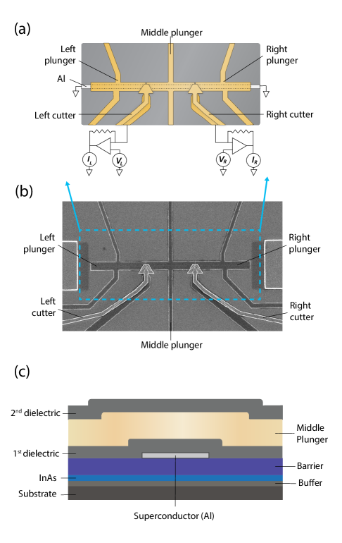
In the DLG design, instead of a split-gate geometry, the plunger gates cover the Al strip completely, as illustrated schematically in Fig. 3a and in an SEM image shown in Fig. 3b. This makes it considerably easier to align the gates with the Al strip. Moreover, the plunger gates have a single role, which is to control the electron density in the 2DEG — to fully deplete it underneath the regions adjacent to the Al strip and to either fully deplete it or to tune it to the lowest sub-band directly underneath the Al strip. The function of controlling the bulk density is separated from the function of opening and closing the junctions, which is accomplished by cutter gates that are in a second gate layer, separated from the first gate layer by a second dielectric layer. The cutter gates in the DLG design only cover the junctions, so they do not affect the bulk density in the wire. Although the above differences between the SLG and DLG designs are practically important, the basic principles and length scales are the same in both.
We will call the semiconductor underneath the middle section “the wire,” and the superconducting gap that is induced in the wire at via the proximity effect the “induced gap” . We denote the middle plunger gate voltage by , which tunes the density in the wire. At the optimal operation point, the wire is tuned to the single-sub-band regime that occurs just before full depletion . We will focus on the phase diagram of the wire as a function of the middle plunger gate voltage and the magnetic field .
We comment briefly on the length of the wire here and discuss it in greater detail in Sec. A.3. To operate the device in the optimal regime, the nanowire should be much longer than the coherence length in the topological superconducting state, so that MZMs are well localized at the opposite ends of the nanowire [the situation depicted in Fig. 2(c)]. In this case, MZMs would lead to ZBPs that are stable with respect to local perturbations. When the coherence length is comparable to or larger than the nanowire length, a ZBP at one end of the wire may arise from an Andreev state extending from the opposite end [92]. In this case, however, we do not expect ZBPs to be stable with respect to local perturbations. Our simulations suggest that, for these designs and material stacks, the coherence length in the topological state would be around 300 nm in the absence of disorder. The wire is designed to be much longer than this. Disorder in the bulk of the nanowire suppresses the topological gap and increases the coherence length which, as we discuss in Sec. A.3, leads to a non-trivial requirement for the wire length which depends on the stack geometry/composition and disorder level. On the other hand, the wire cannot be too long since the visibility of gap closings will be strongly suppressed if the length of the wire is more than several times the normal-state localization length [87].
Assuming weak to moderate disorder, the optimal wire length in our devices is . This length choice also ensures that when a transport gap closing is observed, there is a non-zero density of states in the bulk at zero energy which has non-vanishing matrix elements to both leads so that non-local conductance is above the noise floor [89].
Finally, the outer sections (underneath the left/right cutter/plunger gates) must be significantly longer than the coherence length of the parent superconductor in order to prevent quasiparticle transport below the parent gap at full depletion.
2.3 Material stack
The material stack of the topological gap device is optimized to produce a large topological gap. To achieve a topological phase, the semiconductor stack needs to produce a large spin-orbit coupling and a large nominal -factor in the confined 2DEG. In addition, the heterostructure should provide a low disorder environment, typically parameterized by high 2DEG mobility at low temperatures. Given the lack of suitable insulating and lattice-matched substrates, the active region is grown on an InP substrate employing a graded buffer layer to accommodate lattice mismatch.
The active region consists of the Al superconductor, an upper barrier, the InAs quantum well, and the buffer. The upper barrier layer plays a critical role in fine-tuning the coupling between the superconductor and the 2DEG residing in the quantum well. To drive the device into the topological phase, needs to be increased until the Zeeman energy exceeds the induced gap . Here, is the renormalized -factor in the superconductor-semiconductor heterostructure, which is given by if we neglect the -factor of aluminum; a more general form of the renormalization factor is discussed in Sec. A.1. For strong coupling between the wire and the Al strip, would approach the gap in the Al strip and the electronic wavefunction of the single occupied sub-band of the wire would have large weight in the Al strip. In this case, would be renormalized to small values. In such a case, would not approach until the magnetic field is very large (T), close to the critical in-plane field of the Al strip [27, 93, 59, 94, 95]. Conversely, if the coupling between the superconductor and semiconductor were too weak, the maximum attainable topological gap would be small, since it is bounded above by . Hence, the material stack must satisfy .
As we shall see in Sec. 4, the parent gap in the Al strip is (this is strongly dependent on the Al thickness). For an optimized heterostructure, according to our simulations of the device of Fig. 2(a), we expect , corresponding to an induced gap to parent gap ratio of , and .
Another function of the upper barrier layer is to separate the quantum well states from disorder on the dielectric-covered surface of the stack, thus enhancing the electron mobility. The quantum well thickness is chosen to minimize orbital effects from the magnetic field applied in the -direction, to allow electrostatic tuning, and to retain the desirable properties of InAs, including optimally renormalized .
Rashba spin-orbit coupling in the wire, characterized by the parameter , enables superconductivity to co-exist with the magnetic field . Although does not determine the critical field for the transition into the topological phase, it does contribute to the size of the topological gap and the extent of the topological phase in parameter space. The heterostructure has been engineered to have spin-orbit coupling in the range of to .
In this paper, we present the results of measurements and simulations of devices based on four different material stacks satisfying the requirements given in this subsection. While they all feature an InAs quantum well, there are important differences in the quantum well width, barrier composition and thickness, and dielectric. In Sec. 2.4, we give the effective parameters that encapsulate the effect of these materials changes, such as the the effective mass, -factor, and spin-orbit coupling. We will call these different materials stacks , , , and .
2.4 Phase diagram of ideal devices
For the SLG and DLG device designs described in Sec. 2.2 and the material stacks described in Sec. 2.3, we have computed the phase diagrams in the ideal disorder-free limit as a function of the actual control parameters of the device, and . This is to be contrasted with Eq. 1 and Fig. 1, which contain the effective parameters and . The bare spin-orbit coupling in the semiconductor is taken to be in both the SLG- and DLG- designs. The color scheme in Fig. 4 is determined by the Pfaffian invariant [9, 97] (see Sec. A.4 for a brief description of this invariant). Darker red corresponds to larger topological gap and darker blue corresponds to larger trivial superconducting gap, as indicated by the color scale on the right-hand-side of the figure.
The red parabola in Fig. 1 has now become a sequence of red slivers in the ideal phase diagrams of an SLG device built on the stack in Fig. 4(a) and a DLG device built on the stack in Fig. 4(b). The red slivers are topological phases with different numbers of occupied 1D sub-bands in the wire [98, 27]. When we zoom in on any one of these slivers, we see that it has the parabolic lobe-like shape that follows from Eq. 1. Here, the single-sub-band topological phase is at V, and it has a larger topological gap than when there are more occupied sub-bands. Recall that one of the design criteria was that the single-sub-band regime could be reached for moderate gate voltages; this figure confirms that it is satisfied by this design. As we increase , thereby increasing the number of occupied sub-bands, the effective cross-sectional area of the gate-defined nanowire increases and, at some point, the orbital effect of the applied magnetic field becomes very important. In the second sub-band, an orbital-field-induced gap closing is visible at T and V. It occurs at T in the third sub-band and at lower fields in higher sub-bands. In contrast, in the lowest sub-band, an orbital-field-induced gap closing does not occur over the relevant field range. (At fields higher than T, the Al parent gap can close, so an orbital-field-induced gap closing would be a sub-leading effect anyway.) Thus, in order to maximize both the accessible volume of the topological phase and its maximum gap, it is necessary to tune the device into the single-sub-band regime.
There is very little difference between the SLG and DLG designs in the bulk of the wire; the principle difference is in the junctions, which have no effect on the ideal bulk phase diagram. However, the stack has larger and smaller so the topological phase occurs at higher for this stack. Hence, the DLG- phase diagram in the clean limit has a lowest sub-band topological phase that is pushed to higher fields, as may be seen in Fig. 4.
Within the lowest sub-band, the effective mass , effective Rashba spin-orbit coupling , effective -factor , superconductor-semiconductor coupling , and lever arm take the values given in Sec. 2.4. As a result of the projection to the lowest sub-band, the bare Rashba spin-orbit coupling is replaced by the effective parameter given in the table. The precise definition of the effective single-band model governed by these parameters is given in Sec. A.1.
| Design, stack | |||||
| SLG- | 0.032 | 8.7 | 0.13 | 85 | |
| DLG- | 0.032 | 8.4 | 0.21 | 79 | |
| DLG- | 0.032 | 8.3 | 0.32 | 78 |
2.5 Disorder and uniformity requirements
We now discuss the level of imperfection that our device designs are expected to tolerate and still have a topological phase with coherence length shorter than the wire length . See Sec. A.3 for a discussion of the coherence length and other important length scales.
In our devices, there are many different sources of disorder, including geometric and charged disorder [27, 38, 99]. Even small local variations in any of a number of device parameters can cause significant variations in the potential experienced by the electrons along the wire. As we discuss in Sec. A.1, we can extend the single-sub-band effective model Eq. 5 parameterized by the couplings given in Sec. 2.4 to include disorder, leading to the Hamiltonian Eq. 16. When the various disorder mechanisms are projected into this single-sub-band model, most of them can be characterized by the quenched Gaussian disorder model [100] in which disorder is represented by a random potential whose probability distribution is approximately described by the second-order cumulant defined in Eq. 18. Both the strength of disorder and its correlation length depend on each disorder source in a manner that is highly dependent on the specific design and must be calculated in a full three-dimensional model, as we describe below. The designs in Fig. 2 and Fig. 3 have been optimized to be as forgiving as possible by requiring that the design minimize the projected disorder for fixed microscopic disorder.
In the regime of interest — the low-density regime with single sub-band occupancy — charged disorder dominates [101]. From an analysis of the density-dependence of the mobility of Hall bars, we conclude that charged disorder is located primarily at the interface between the semiconductor surface and the gate dielectric. Hall bar measurements allow us to extract the average density of charged imperfections at the semiconductor-dielectric interface, denoted by , and the lever arm . This is illustrated in Appendix B. Each chip studied in this paper has both topological gap devices and Hall bars, as shown in Fig. 5, enabling us to extract the average density of charged imperfections for each chip and to assess the impact on topological gap devices of chip-to-chip changes in the disorder level. Any impact that post-growth fabrication has on the semiconductor-dielectric interface in a topological gap device will be present in its partner Hall bar as well since they are processed together on the same chip. If any fabrication processes increase the density of charged imperfections in a topological gap device, we will detect this in the corresponding Hall bar.
We have optimized the device geometry with respect to charged imperfections at the semiconductor-dielectric interface by choosing the Al width as wide as possible while still maintaining the ability to tune into the single sub-band regime. This keeps the active region in the InAs quantum well as far as possible from charged disorder at the interface between the semiconductor and the dielectric [see Fig. 2(d)]. (As we discussed in Sec. 2.3, the barrier layer plays a similar role in separating charged disorder as much as possible from the active region.) We use self-consistent electrostatics calculations [59, 60] to find the disorder potential underneath the Al. For realistic densities of charge defects , we find the variance of the projected disorder potential and correlation length to vary between -1.5 meV and -125 nm, respectively. In Fig. 22, we show how depends on for the SLG and DLG designs of, respectively, Fig. 2 and Fig. 3 in the , , or stacks.
From a transfer matrix calculation of for the model in Eq. 16, we can obtain the disorder strength at which the minimum value of the coherence length begins to exceed our device length. Fig. 22 enables us to translate that value into a target . In particular we obtain for SLG- parameters that this occurs for . The and stacks have slightly different requirements as a result of their stronger coupling to the superconductor, (which is still within the required range of ). Hence, an initial target for dielectric quality is . In this paper, we show data from devices that are below and above this target. The topological phase is present in the thermodynamic limit even for relatively high disorder, but with large , which renders it unusable in an wire. The condition that is significantly more restrictive. As we shall see when we consider the case of a single disorder realization in Sec. 2.6, the condition that the gap not be too small is also more restrictive.
We estimate that the corresponding bound on the peak mobility (as a function of density) for Hall bar devices fabricated on the same material stack is at electron densities -. The 2DEGs used in this paper have peak mobility in the range 60,000-100,000 in this density range. Additional details are in Appendix B.
In a similar fashion, we have optimized the design with respect to other disorder mechanisms including variations of the following parameters along the length of the wire: thickness and dielectric constant of the oxide, barrier thickness and composition, wire width, quantum well thickness, buffer composition and thickness. We have extracted these disorder parameters from measurements and used them in our simulations of topological gap devices. We have also taken into account disorder induced by imperfections in the substrate and as well as disorder resulting from inhomogeneous superconductor growth.
2.6 Topological phase diagram for a single disorder realization
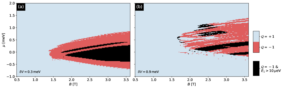
Even when a device satisfies the requirements explained in the previous subsection and has a topological phase, disorder can cause the shape of the phase diagram to be rather complicated. To gain a getter understanding, it is helpful to examine the phase diagram for a few representative disorder realizations. In this section, we diagonalize the Hamiltonian in Eq. 16 and calculate the Pfaffian topological invariant [9, 97] for two independent disorder realizations. In any finite-sized system, the disorder-driven phase transition between the topological and trivial phases is rounded into a crossover. Consequently, a topological phase can be found in the phase diagram in some percentage of devices even for average disorder levels that exceed the critical value obtained in the thermodynamic limit. Conversely, some percentage of devices will not have a topological region of the phase diagram even for average disorder levels for which there would be a topological phase in the thermodynamic limit. Although disorder induces low-energy states — by creating domain walls between topological and non-topological regions, for instance — the density of such states may be low enough that an appreciable fraction of even reasonably long devices may not have any. Thus we can also characterize the phase diagram by the spectral gap in the region, taken as the second-lowest eigenvalue of (the lowest corresponds to the Majorana zero mode pair splitting).
In Fig. 6, we show the phase diagrams of two different simulated devices. Both have the DLG- design, but with two different disorder realizations, one with meV (panel a) and one with meV (panel b). For weak disorder, the lobe structure of the topological phase is preserved, and the spectral gap remains high over a large region inside the lobe. For stronger disorder, mesoscopic fluctuations are important, as we discuss in Sec. A.3. The parabolic-shaped lobe of the topological phase of Fig. 1 — as identified by the Pfaffian topological invariant — is splintered into several disconnected regions of narrow range in and larger extent in . This effect is even more dramatic if we additionally condition on a large spectral gap (black regions in Fig. 6). We will call these long, narrow regions of topological phase splinters of the single-sub-band lobe.
2.7 Statement on confidential information
In summary, the principles behind the design of our devices and material stacks are that they should enable three-terminal transport and: (1) be based on a 2DEG residing in a low-defect quantum well; (2) have a charged defect density at the semiconductor-dielectric interface that is less than , as measured on a Hall bar on the same chip; (3) allow tuning to the lowest sub-band and full depletion of the wire; and (4) have an induced gap to parent gap ratio in the lowest sub-band that satisfies .
The barrier thickness and composition, quantum well thickness, dielectric composition and deposition method, and Al strip width are critical factors that determine whether a device meets these prerequisites. The details of these design parameters and fabrication methods are Microsoft intellectual property that we cannot disclose. However, the principles listed above and described in this Section (particularly Secs. 2.2, 2.3 and 2.5) are sufficient to determine the key design and process parameters through a combination of simulation and experimentation. In particular, Hall bar measurements can be used to measure progress towards satisfying requirements (1) and (2); while zero-field transport measurements of topological gap devices (described in the next section) can be used to determine when (3) and (4) are satisfied. We present such measurements directly verifying that the , , , and material stacks in either SLG or DLG designs fulfill them.
All of the key material and design parameters feed into the effective parameters given in Sec. 2.4, together with and . They define the projected single-sub-band model in Eq. 16 from which our simulations can be reproduced. Any device that replicates our design and material stack will have similar effective parameters.
3 Topological gap protocol
The goal of the TGP is to identify whether there are regions in the experimental parameter space that show signatures consistent with a topological phase. The full source code of the TGP and raw data sets are available in Ref. 96. The device’s outer sections are kept in the trivial superconducting phase by tuning their densities with the right and left plunger gates. In the topological phase of the wire, MZMs are localized at the boundaries between the topological and trivial sections, see Fig. 2(c). Provided that is smaller than or, at least, not too much larger than the localization length , see Sec. A.3, there will also be an observed non-zero bulk transport gap. When this condition is satisfied, a non-zero above-gap non-local conductance is observable, enabling an identification of the gap, as we discuss further in Sec. A.3. In the TGP [8], the presence of MZMs and a bulk transport gap is detected by measuring the differential conductances
| (2) |
as a function of and as well as the voltages controlling the tunnel junction transparencies, and the bias voltages , which can be increased in order to tunnel current into states of higher energies. The currents and voltages are illustrated in Fig. 7. We use the cutter gates to open and close the junctions; when is more negative, the junction is more closed, and similarly with . We discard all devices in which one of the junctions cannot be completely closed at a pinch-off voltage V. Even among devices that pass this basic health check, there is considerable device-to-device variation in the pinch-off voltages and, more generally, in the relation between , and the conductances through the junctions. This is, presumably, due to the different disorder configurations in the different junctions; these differences have a large effect because the junctions are depleted, leaving charged impurities unscreened, unlike in the bulk of the wire where the Al strip can suppress the effects of charged impurities via screening.
We want to vary the cutter gate voltages so that the local electrostatic environments at the two junctions change by enough to change the energy of bound states that are accidentally at zero energy for one cutter gate configuration. But since the cutter gate voltage change required to open or close a junction varies significantly from one junction to another as a result of disorder, we cannot simply choose the same sequence of , values for each device. Instead, we use the above-gap conductance at and a bias voltage of as a measure of the junction transparencies. In each device, we find sequences of cutter gate voltages , for which at both junctions take values between and . They are slightly different in each device, but they always cover a substantial fraction of this range. When we say, as a shorthand, that we are varying the junction transparencies, we mean that we vary , in this manner.
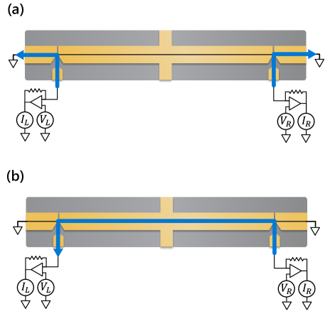
In the tunneling regime (i.e. for ), the current paths contributing to , are illustrated in Fig. 7(a). In this regime, and directly measure the local density of states in the wire at the boundaries between the middle and, respectively, the right and left sections. Hence, ZBPs in and in the tunneling regime indicate the presence of zero-energy states in the wire with sufficient tunneling matrix elements to the leads, consistent with MZMs but also with trivial zero-energy Andreev bound states. A zero-energy state (either MZM or trivial ABS) at the right junction will be manifested as a ZBP in and similarly for a zero-energy state at the left junction and a ZBP in . Trivial ABS are not generically stable with respect to local perturbations whereas well-separated MZMs are. Therefore, the ZBP stability criterion, discussed below, allows one to better identify the region of interest.
The current path contributing to is illustrated in Fig. 7(b); is determined by the reverse path. For an intuitive understanding of and , we first note that in the thermodynamic limit of the wire, the clean limit, and the tunneling limit of both junctions, a current injected at bias voltage above the Al parent gap will flow through the Al strip to ground via the contacts at the ends of the device unless it relaxes to energies between the induced gap and the parent gap. Hence, at bias voltages above the Al parent gap, and are strongly suppressed and are non-zero only as a result of these weak relaxation processes [87, 89, 102]. At zero-temperature, in the thermodynamic limit of the wire, the clean limit, and the tunneling limit of the junctions, current cannot be injected into the wire at bias voltages below the induced gap, except by Andreev processes, which inject supercurrent that also flows to the grounded contacts at the ends of the device. Now consider a finite-length disordered wire. At bias voltages at which the localization length is less than the length of the wire, and are strongly suppressed and are non-zero only as a result of non-zero temperature and finite ratio . (In an infinite wire, and would vanish at all bias voltages because all states are localized, except precisely at the transition. For a further discussion, see Sec. A.3.) Consequently, the highest bias voltage below which and are nearly vanishing (in a sense that we make more precise below) can be interpreted it as the transport gap that we define in Sec. A.3. As we discuss in Sec. C.1, we perform this gap extraction with the parts of the non-local conductances that are antisymmetric in bias voltage, , :
| (3) |
and similarly for .
The high-dimensional nature of the parameter space that is explored by the TGP makes it prudent to narrow the measured parameter range. We explained above how the range of junction transparencies is limited. Meanwhile, the parameter range of is chosen to be close to the bottom of the first sub-band. When the chemical potential is below the first sub-band, the wire is fully depleted. The depletion point is identified by scanning the non-local conductance as a function of bias and . This can be done at or at non-zero , with below the critical field of the superconductor, where the signal is generally larger. Recall that, as noted above, the non-local conductances are essentially zero outside the range of bias voltages between the induced and parent gaps, except for finite-size effects, thermal activation, and relaxation effects. Hence, full depletion of the wire causes the non-local conductance at bias voltages below the Al gap to drop below the noise floor. We use this depletion point to identify the single-sub-band regime.
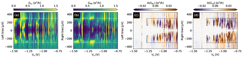
In Fig. 8, we show the four elements of the experimentally-measured conductance matrix as a function of bias voltage and plunger gate voltage at zero magnetic field in one of our devices, which we label device A, to illustrate how the depletion point is identified. As may be seen from Fig. 8(c,d), the anti-symmetrized non-local conductances are small above the parent gap , which is indicated by horizontal dotted lines in Fig. 8(c,d). The anti-symmetrized non-local conductances are non-vanishing down to small bias for V, which indicates that there is conduction through 2DEG regions not contacted by the Al for these plunger gate voltages. For more negative than V, these 2DEG regions are depleted, and the induced gap opens up. As discussed previously, the anti-symmetrized non-local conductances are large between the induced and parent gaps, are suppressed above the parent Al gap, and are very strongly suppressed below the induced gap. As is decreased further, the induced gap increases, eventually reaching its maximum measured value of . At V, the anti-symmetrized non-local signal drops sharply while local conductances remain large. For more negative , the anti-symmetrized non-local signal is very small, and there is no longer a visible bias range between the induced and parent gaps. This is interpreted as full depletion of the semiconductor below the Al strip. The single-sub-band regime occurs just before wire depletion.
In summary, the TGP makes the parameter space of our devices manageable by by focusing on the most favorable region: near the bottom of the lowest sub-band; from zero up to T; and a range of junctions transparencies between and .
The steps of the TGP are divided into two stages. Stage 1: (1) From an analysis of and , identify ZBPs at each end of the wire that are stable to variations of the junction transparencies and variations in local junction potential (which are controlled by , in the manner discussed above). (2) Find clusters of points in the - plane where there are stable ZBPs at both ends of the wire. These clusters and their surrounding neighborhoods define the regions of interest ROI1 that are the focus of Stage 2. If there are no such clusters, the device fails Stage 1.
Stage 2: (3) Focusing on smaller ranges containing ROI1s and restricting to cutter gate voltage pairs for which the junction transparency is approximately the same at both ends, confirm the existence of stable zero bias peaks in and and recover the clusters of points in the - plane where there are stable ZBPs at both ends of the wire. This step is important when there is a drift in between Stages 1 and 2. (4) Use and to determine the bulk energy gap as a function of for each cutter gate pair. (5) For each cutter gate pair, find ZBP clusters identified in step 3 whose interiors are gapped and whose boundaries are gapless. We will denote them by where is a cutter gate pair index and is an index that distinguishes different gapped ZBP clusters with gapless boundaries that might occur for the same cutter gate pair. (6) Find the sets of clusters in the - plane consisting of that overlap for different cutter gate settings. To be more precise, we define . The device passes the TGP if there is a such that there is a for a number of cutter gate settings that exceeds some threshold, as we make more precise in Sec. C.2. In this case we define the region of interest . Note that for a given device, there can be several ’s and s. We will call the clusters “subregions of interest SOI2 belonging to a region of interest ROI2.”
There are a number of important measurement complexities that we discuss in Sec. C.1. The TGP is formulated with several thresholds which we explain in Sec. C.2: the minimum percentage of cutter gate settings for which a ZBP must be present in order to be considered stable, denoted by ; the minimum percentage of the boundary of a ZBP cluster that must be gapless in order for the whole boundary to be considered gapless, denoted by ; the conductance value below which we consider it to be effectively zero up to finite-size effects, denoted by ; and the minimum percentage of cutter gate settings for which an overlapping SOI2 must be present in order to form an ROI2, denoted by .
The TGP captures the key physics of topological superconductivity because it requires a device to show stable ZBPs at both ends and also a bulk gap closing and re-opening. However, we can make a much stronger quantitative statement about its reliability by testing it on simulated devices. We simulated 349 devices of different designs, material stacks, and disorder levels and applied the TGP to transport data from these devices. To test its reliability, we compared the ROI2s located by the TGP with the “scattering invariant” [103], a topological index that is defined for open systems (see Sec. A.4 for a brief description of this invariant). When the topological index is in some region of the phase diagram, the region is topological; when it is , the region is trivial. However, trivial regions of the phase diagram can exhibit relatively stable ZBPs in their transport data, and the TGP was designed to avoid misidentifying such regions as topological.
We classify ROI2s as true positives (TP) if they contain any region with non-trivial topological index and as false positives (FP) otherwise. The false discovery rate (FDR) is the probability that an ROI2 is trivial:
| FDR | ||||
| (4) |
where is the total number of devices. In essence, the FDR is the probability that if a device passes the TGP then the ROI2 that it identifies has a completely trivial explanation, such as a trivial ABS. We estimate the FDR from the TP and FP numbers obtained from a large — but finite — number of simulated devices. As , the ratio approaches the FDR. For finite , the best that we can do is estimate upper and lower bounds on the FDR. We use the Clopper-Pearson confidence interval at the 95% confidence level to estimate these bounds.
Our results are shown in Sec. 3. Since we found no false positives, the confidence interval for the FDR is between zero and the upper bound that we list in the rightmost column. We find that if a device passes the TGP, there is a probability that the ROI2 that it finds does not contain a topological phase. For the DLG- design, the probability is . We simulated several different disorder levels to investigate whether the TGP is more likely to give false positives when disorder is higher. Our results indicate that the TGP is reliable over the entire range -, which is the range of charged disorder levels in the measured devices discussed in Sec. 4.111Note that the threshold depends on the level of disorder in the system and is taken differently at charged disorder compared to the other cases. See Appendices D.2 and D.3 for details. Similarly, the differences between the SLG- and DLG- stacks and designs have no effect on the accuracy of the TGP. The small dependence of our FDR estimates on disorder level and design that may be seen in Sec. 3 are entirely a consequence of the different numbers of ROI2s that were found at different disorder levels. Further details are given in Appendix D. As we discuss in Sec. 5, the statistical properties of the ROI2s that we find in our simulations agree with the corresponding experimental values, thereby further validating the simulation model used estimate the FDR. This analysis addresses open questions regarding the reliability of the TGP [104].
| Design, stack | TP | FP | FDR | |
| SLG- | 1.0 | 244 | 0 | |
| 2.7 | 46 | 0 | ||
| 4.0 | 45 | 0 | ||
| DLG- | 0.1 | 125 | 0 | |
| 1.0 | 97 | 0 | ||
| 2.7 | 67 | 0 | ||
| 4.0 | 66 | 0 |
4 Experimental data
4.1 Measurements of device A
In the remainder of this paper, we focus on measurements of devices such as the one shown in Fig. 2. In this section, we focus on data from device A, which is a long SLG device built on a -stack. We discuss three experimental measurements from this device. The raw data is available in Ref. 96. Measurement A1 was taken in one dilution refrigerator while measurements A2-A3 were taken in a different cooldown of device A in a different dilution refrigerator. The measured zero-field superconducting gap in the Al strip is and the maximum induced gap at zero -field is , which indicates that the induced gap to parent gap ratio is well within the desired range. The effective charged impurity density at the interface with the dielectric is , as is discussed in Appendix B. This value satisfies the specification explained in Sec. 2.5, which is based on the assumption that the average charged impurity density at the dielectric-semiconductor interface in the Hall bar is the same as at the dielectric-semiconductor interface in a topological gap device (the boundary between light blue and grey on either side of the Al strip in Fig. 2(d)) on the same chip. The critical field, , for the thin Al strip is T for magnetic fields in the direction of the strip. The single sub-band regime, as determined from the non-local conductance in the same manner as in Fig. 8, is reached at between and V (depending on the cooldown). This is consistent with our simulations for device A; see Fig. 4. The base temperature in our measurements is mK and, using NIS thermometry [105], we measured an electron temperature mK.
4.1.1 TGP Stage 1
We begin by finding the single-sub-band regime, following the method discussed in Sec. C.1. The non-local signal below the Al parent gap vanishes for V, which we interpret as the point at which the wire is fully depleted. We focus our Stage 1 scans on a range of mV above this value.
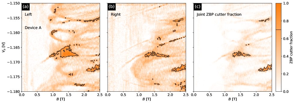
In Fig. 9(a,b), we show the cutter gate fraction for ZBPs at, respectively, the left and right junctions as a function of and . The black lines in Fig. 9(a,b) encloses the regions in which the cutter gate fraction for ZBPs at the left or right junction is greater than . Finally, in Fig. 9(c), we show the fraction of junction transparencies at which there are ZBPs at both junctions, plotted as a function of and . The black line indicates the part of the phase diagram where the cutter gate fraction for ZBPs at both junctions is . Stage 1 data was taken for 5 different cutter gate voltages at each junction, or in total 25 settings. The cutter gate voltages were chosen so that of each junction is in the range -. In Stage 1, we find values at which there are ZBPs at both junctions for more than out of pairs or, in other words, for which the cutter gate fraction for ZBPs at both junctions is . Clusters of such points are the candidate regions of topological phase yielded by Stage 1 of the TGP, dubbed ROI1 in Ref. 8.
There are several key features in Fig. 9 worth emphasizing. First, we expect that the topological phase in proximitized nanowires should have a lobe-like shape in the absence of disorder. As a result of disorder, we expect the lobe to be splintered, as shown in the simulations in Fig. 6. In Stage 1 data from simulated device R1, this manifested as splintered regions in which there are stable ZBPs at both ends of the device, as may be seen in Fig. 27. The mV field of view in Fig. 9 corresponds to a single lobe,which we identify as the lowest sub-band according to the method discussed in Sec. C.1.The structure that is visible in the phase space locations of stable ZBPs at the left and right junctions and, especially, in ROI1 resembles the splintering of the lobe.
We have observed very similar ROI1s in several devices (such as devices B, C, D, and E). In more disordered devices (such as device F, which is discussed in Sec. 4.2), ZBPs are scattered throughout phase space, and there is no structure, which suggests a non-topological phase of matter.
The data is reproducible between successive measurement runs on the same device, as we show in Sec. 4.1.3. The system is very stable, provided that is varied by mV or less. If the voltage is varied by more than mV, features shift in but we can recover the same ROI1. If a device idles for approximately a week near an ROI1, we find that voltages drift by at most a few mV, as we will see when we compare measurements A2 and A3.
We emphasize that the main goal of Stage 1 is to identify promising regions in parameter space for measurements of both the local and non-local conductances over a range of bias voltages, which are the focus of Stage 2.
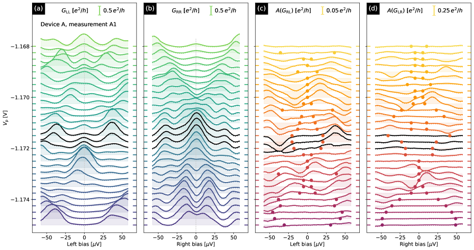
4.1.2 TGP Stage 2: Measurement A1
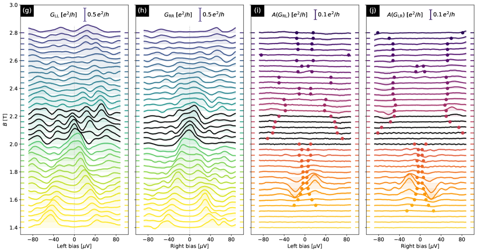
In Stage 2, we focus on the regions of the - plane where there are clusters of points with stable ZBPs at both junctions. We map out the full conductance matrix Eq. 2 as a function of , , , , and, in addition, . Since we are now exploring a higher-dimensional parameter space, we restrict the sweep to the vicinity of ROI1 identified in Stage 1, which is typically -mV. We further restrict the parameter space by taking scans for 3-5 cutter gate pairs (rather than the 25 pairs of Stage 1). In the measurement of device A displayed in Fig. 10, there were 3 cutter gate pairs . These cutter gate settings correspond to of , , and at both junctions. In Fig. 10, we show data for the representative cutter gate setting for which for both junctions and the discussion below focuses on this data. Qualitatively similar observations hold for the other two settings.
Since, as was previously mentioned, there is typically a small voltage drift between Stages 1 and 2, we start the analysis of the Stage 2 data by determining the regions with stable zero bias peaks anew. We call the ZBPs stable if they are present for at least 2 out of 3 cutter gate settings. In Fig. 10(c,d), we illustrate ZBPs for our representative cutter gate setting by showing and for V. In Fig. 10(b), we see that the corresponding horizontal line passes through a region with stable ZBPs, indicating that these ZBPs are present at least one other cutter gate setting as well. The and data shown in Fig. 10(c,d) is displayed as “waterfall” plots in Fig. 10(g,h), which is an alternate but equivalent method of representing the same data. We re-emphasize that the conductances , are not topological invariants and are not expected to have quantized values at non-zero temperature and non-zero junction transparency. So a ZBP, no matter how stable or well-quantized, cannot prove that the system is in a topological phase. Conversely, the existence of a topological phase in a device is not disproven by a ZBP that has a small magnitude, such as the ZBPs at the left junction in Fig. 10(c,g). In the TGP, we classify ZBPs by their stability to parameter changes. In particular, ZBPs that are stable with respect to changes of the cutter gate voltages is a mandatory requirement of the TGP. We give an example from a Stage 2 measurement in Fig. 14.
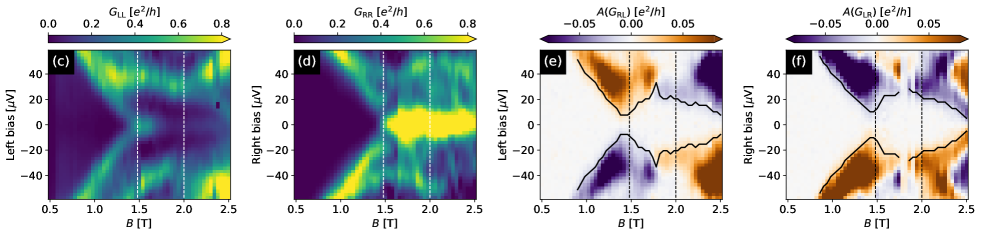
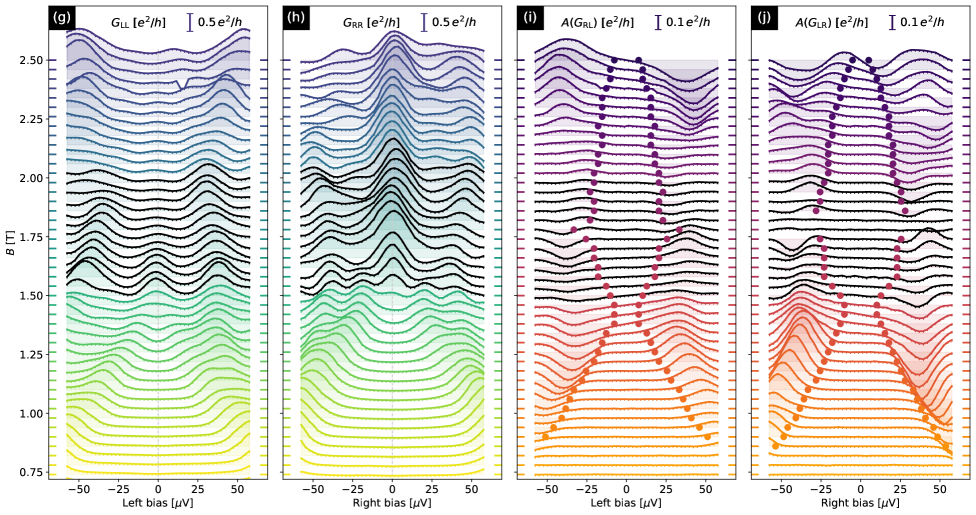
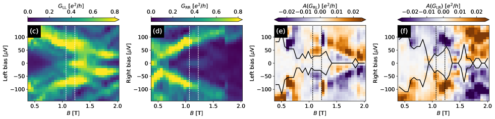
Next, we use bias scans of the non-local conductances , to determine the bulk transport gap at each point in the phase diagram. We illustrate this in Fig. 10(e,f), where we show and as a function of at the V horizontal line in Fig. 10(b). The black curves in Fig. 10(e,f) show the transport gap extracted from, respectively, or as a function of for this value. The black curves are determined according to the procedure explained in Sec. C.1. The transport gap is obtained by taking the minimum of the values extracted from and . There is a clear bulk transport gap closing and re-opening visible in at T. The gap remains open from T to T.
We further illustrate the behavior of , by taking a vertical cut through the - plane. In Fig. 11, we show waterfall plots of local and non-local conductances as a function of at fixed T. The black dots in Fig. 11(c,d) indicate the bulk transport gaps extracted from and . A gap closing and re-opening is clearly visible in these plots. We emphasize that these cuts through the phase diagram are a very small sample of the data comprising Stage 2 of measurement A1.
While these illustrative cuts are highly enlightening, they are not the primary goal of Stage 2 of the TGP, which is to derive an experimental phase diagram from the measured conductance matrix as a function of , , , , and . The TGP yields the experimental phase diagrams in Fig. 10(a,b) for our representative cutter gate setting. All three cutter gate settings yield similar phase diagrams. The color scheme in Fig. 10(a,b) is the same as in the simulated phase diagrams in Fig. 28(a,b). The most salient feature of Fig. 28(a,b) is the presence of an SOI2. In this region, there are stable ZBPs at both ends of the device, and there is a non-zero bulk transport gap; 78% of the boundary of this region in the - plane is gapless. Device A passed the TGP.
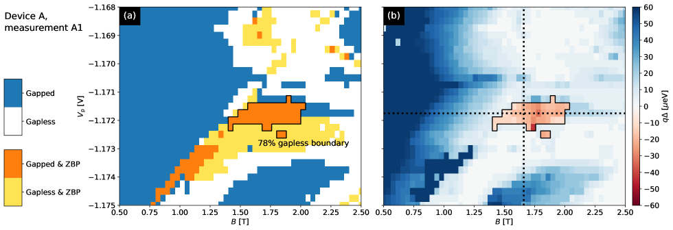
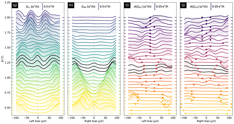
The crucial point of the TGP is to not rely on a single feature to identify a topological phase, but instead to rely on the totality of the data to provide evidence for the observation of a topological phase. Indeed, each pixel in Fig. 10(b) is determined by conductance data in a neighborhood of points around that pixel and for a range of cutter gate settings.
From , , we infer a bulk gap closing and re-opening, which is a signature of a second-order phase transition. It is important to distinguish such behavior in the non-local conductances , from apparent gap closings/re-openings in the local conductances , , which could easily be the motion of a local state towards zero energy, rather than a bulk phenomenon.
This phase transition line separates the high-field gapped phase from the gapped trivial superconducting phase that is present at low fields. It does not quite surround the high-field gapped phase: 78% of the boundary shows a gap closing in , . This surpasses ; it is similar to the percentage of the boundary of the SOI2 that is gapless in the simulated data of Fig. 28 and is typical for simulations of this device design and disorder level. Consequently, we believe that the second order phase transition line that surrounds 78% of our putative topological phase is, in fact, part of an unbroken transition line surrounding the entire phase. As noted in our discussion of in Sec. C.2, one possibility is that the gap closing is not visible along 22% of the boundary of the SOI2 due to a suppression of the signal by disorder/non-uniformity while another is that the topological region is larger than the SOI2. Indeed, for the cutter gate setting shown in Fig. 10, there are ZBPs at both junctions up to T.222At the left junction, this ZBP is small, but above the measurement resolution, as may be seen in Fig. 10(c,g). However, at the other cutter gate settings, there is no visible ZBP at the left junction.
The high-field gapped phase is characterized by stable ZBPs at both ends of the wire, which is consistent with the topological phase. For some values, the ZBPs appear before the gap re-opens, including at the V horizontal line in Fig. 10(b). This is consistent with a scenario in which quasi-MZMs [46, 47, 48, 49, 50, 51] are precursors to the transition into the topological phase, which is frequently seen in simulations.
The maximum topological gap is for this cutter gate setting.333The extracted gap can depend on the cutter gate setting. Stability of the gap extraction with respect to cutter gate setting is not a requirement of the TGP. Over the SOI2, which has an extent of mT, mV, the extracted topological gap increases from zero to in such a way that its median value over the region within the black line in Fig. 10(a,b) is . From the phase diagram in Fig. 10(a,b), we see that the lowest field at which the gap closes near the SOI2 is T, which implies an effective -factor of at least . Here, we define , where is the lowest field at which the gap closes.444Here we define the effective -factor as the average slope of the extracted induced gap vs -field. This is different from the conventional definition of the spin -factor in terms of at . The former depends on spin-orbit coupling and orbital physics whereas the latter does not. However, in the single sub-band regime, where the lowest energy state has momentum close to , both the orbital effect of the field and spin-orbit coupling effects are small. In this case, is a good proxy for . This value of is close to the optimal value for this device design and material stack.
The induced gap (and all structure associated with its closing/re-opening) decreases rapidly when the magnetic field is rotated away from the direction of the wire, as expected. The transition to the topological phase should become more smeared as the temperature is increased, but it is difficult to study this systematically due to voltage drifts.
Comparing the experimental data in Fig. 10 to the simulated data in Fig. 28, we note both the qualitative and quantitative similarity between the phase diagrams. In both simulated and measured data, there are gap closings at similar -dependent -field values, and the extent of both the gapless regions and the SOI2s are of similar size in the - plane. However, we emphasize again that the main role of simulated data such as that shown in Fig. 28 is to test the TGP on (simulated) devices for which we know the phase diagram and not to reproduce the experimental phase diagram.
4.1.3 Reproducibility of the data: Measurements A2 and A3
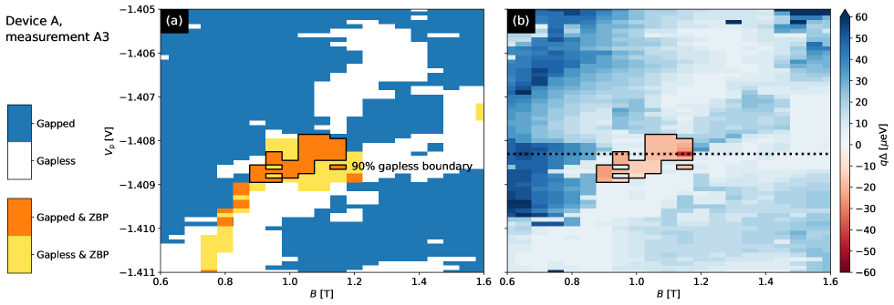
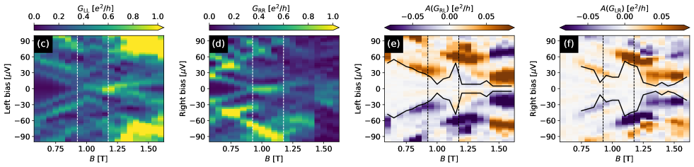
We now present experimental data from a different cooldown in which measurements A2 and A3 were performed one week apart. These measurements produced similar data sets, both passing the TGP, indicating the reproducibility of our data and the device’s stability from one measurement run to another. Both of these data sets are consistent with measurement A1 shown in Sec. 4.1.
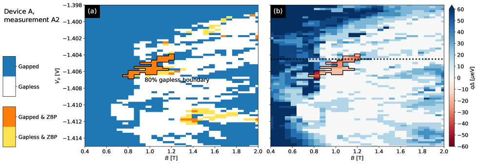
In our simulations, we saw that devices can pass the TGP for some disorder configurations but not others. Each cooldown typically leads to a somewhat different disorder configuration, resulting, for example, in a shift of the gate voltages at which we see the depletion of the lowest sub-band. As mentioned previously, when the device idles for a week, the disorder configuration can also drift slightly. Hence, we expect that the same device will pass the TGP in some measurements but not in other measurements occurring a week or more apart or in different cooldowns. This was the case with device A. It regularly passed the TGP, but also failed sometimes. In this subsection, we focus on measurements A2 and A3, in which device A passed the TGP with a topological phase that shifted in parameter space. For measurement A2, device A was warmed-up, removed from the dilution refrigerator in which A1 was performed, cooled down in a different dilution refrigerator, and re-measured. In accordance with the TGP, we performed Stage 1 measurements and identified an ROI1 with stable ZBPs near V. The results of the subsequent Stage 2 measurement are shown in Fig. 12.
The phase diagrams in Fig. 12(a,b) have the same basic features as those in Fig. 10(a,b). The primary differences are as follows. The lowest gap closing point in A2 is slightly lower in field than in A1, leading to an effective -factor of . The topological phase starts at lower fields, close to 0.8 T, which is closer to the lowest fields at which the gap closes than in A1, and it extends over a larger range of plunger gate voltages, mV but a similar magnetic field range mT. The maximum topological gap in measurement A2 is , see Fig. 12(b), which is the largest observed for device A, and the percentage of the boundary that is gapless is 80%. The local conductances are shown in Fig. 12(c,d). In addition to ZBPs, there is also a strong local resonance at the right junction which is evident in Fig. 12(d). However, this resonance moves away from zero bias as is increased. Furthermore, this resonance disappears in the subsequent measurement shown in Fig. 13(d), indicating that this is an accidental feature due to an impurity that moved between measurements A2 and A3. This trivial resonance partially obscures the stable ZBP, which has a smaller amplitude.
In Fig. 13, we show measurement A3 which was performed in the same cooldown as measurement A2 but one week later. The electrostatic environment of the system drifted by 2-3 mV during the week between the two measurement runs, as is typically the case in our devices. However, the main qualitative features are reproduced from one run to the next: there is a topological phase with a comparable critical field and similar overall shape. The size of the maximum topological gap has decreased from its value in A2 to , which is close to value found in measurement A1.
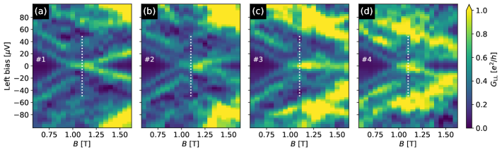
Finally, we discuss the stability of ZBPs with respect to local perturbations. In Fig. 13(c,d) one can see stable ZBPs at both junctions over a magnetic field range T. They are similarly stable with respect to changes in , as may be seen from the vertical extent of the orange region in Fig. 13(a). These peaks are also stable with respect to cutter changes modulating the transparency of the junctions, as we show in Fig. 14. There are ZBPs with height that are present for 4 cutter gate settings. These changes in left cutter gate settings tune on both sides to vary over the range and . Thus, while these cutter changes significantly modify the junction transparencies, the ZBPs remain stable with respect to these perturbations. In SOI2, there are ZBPs exhibiting this type of stability at both junctions.
To conclude this subsection, we believe that the totality of the data from device A — passing the TGP in multiple cooldowns and re-measurements, qualitative and quantitative consistency with simulations, and the stability of the SOI2 with respect to various perturbations — provides strong evidence for the observation of a stable topological superconducting phase supporting MZMs in this device. We now turn to the reproducibility of these results in other devices.
4.2 Experimental data from other devices
Since disorder can destroy the topological phase, and different devices will have different disorder realizations, we can expect quantitative and qualitative differences between devices. Indeed, we have measured devices in which we were not able to find a topological phase. However, devices that have a narrow Al strip, zero-field induced gap to parent gap ratio in the required range, and weak disorder often pass the TGP while devices not meeting these requirements have never passed TGP, as expected from simulations. For example, no devices with dielectric charge density above , as extracted from a Hall bar on the same chip, have passed TGP.
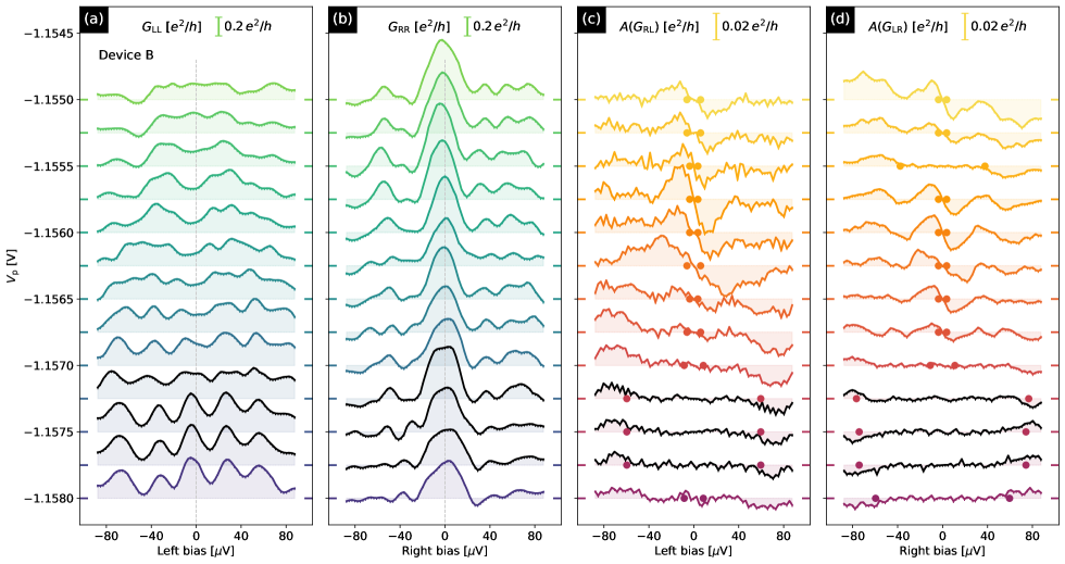
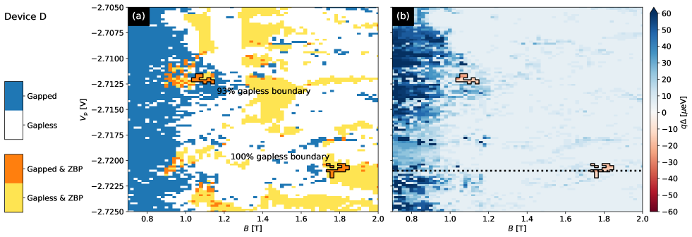
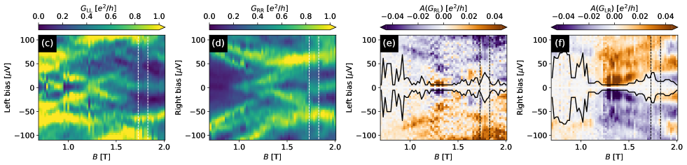
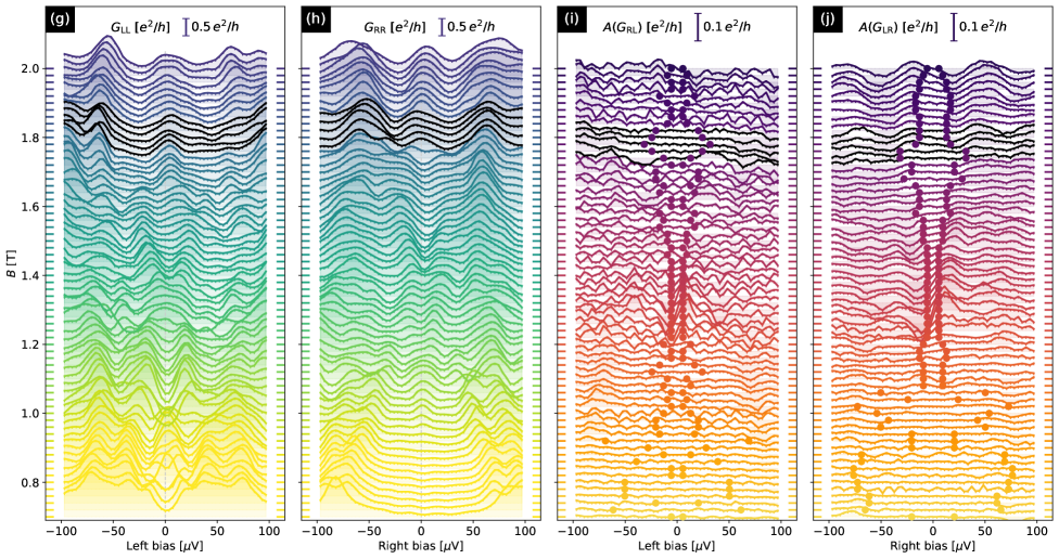
In this section, we show data from devices B, C, and D, summarized in Figs. 15, 17 and 18, which also pass the TGP, thereby demonstrating that we can reproducibly fabricate devices passing the TGP. These three devices are DLG devices. Device B is built on the -stack and has and ; hence, the ratio of the induced gap to the parent gap in device B is 0.52, which is slightly larger than in device A and very close to optimal. It has the largest topological gap reported in this paper: . Device C is built on the -stack and has and ; in device D, which is also built on the -stack, the corresponding gaps are and . The ratio of the induced gap to the parent gap in devices C and D, 0.35, and 0.4, respectively, is somewhat smaller than the nearly-optimal value of 0.52 that it takes in device B or even the value of 0.44 that it takes in device A. The effective charged impurity densities at the interface with the dielectric are in device B, in device C, and in device D, extracted by the procedure discussed in Appendix B.555There is one subtlety here, which is that DLG devices have two different dielectric layers, one below the first gate layer and one between the gate layers. The first dielectric layer is likely to control bulk properties of the wire while both dielectrics contribute to junction properties. The quoted numbers are for Hall bars with both dielectric layers, but the difference with extracted from sibling chips is small. These values are smaller than in device A and satisfy the specification given in Sec. 2.5.
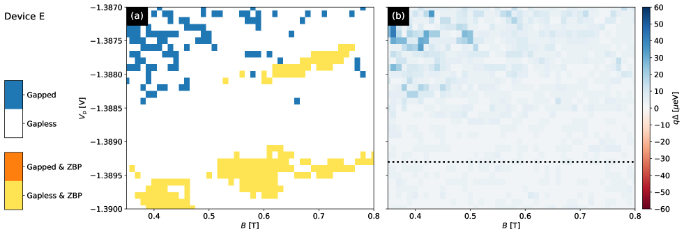
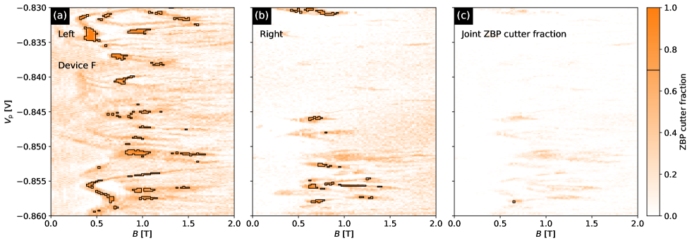
In addition, we show data from devices E and F that do not pass the TGP. They are DLG devices built on the stack. As noted previously, we do not expect all devices to pass the TGP, even if they were to have the same gap ratio and disorder levels as device A. Hence, it is not surprising that some of our devices fail the TGP; indeed, it is required by consistency with our simulations. Moreover, devices E and F have lower induced gap to parent gap ratios, which suppresses their expected probabilities of passing the TGP. Device E has and (induced gap to parent gap ratio of 0.22); in device F, the corresponding gaps are and (induced gap to parent gap ratio of 0.27). The effective charged impurity densities at the interface with the dielectric is in device E and in device F, extracted by the procedure discussed in Appendix B. These values are larger than in devices A-D, and, moreover, are large enough that do not satisfy the specification given in Sec. 2.5.
Device E exhibits clusters of points in space with stable ZBPs at both ends, thereby passing Stage 1 of the TGP. However, non-local conductance measurements in the region of interest yield zero gap. Device E is, thus, in a gapless phase and it fails Stage 2 of the TGP. Device F fails even Stage 1 because it does not have clusters of points with stable ZBPs at both ends.
Overall, the measurement data from devices A-F demonstrate the different qualitative phenomena observed in our devices.
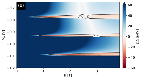
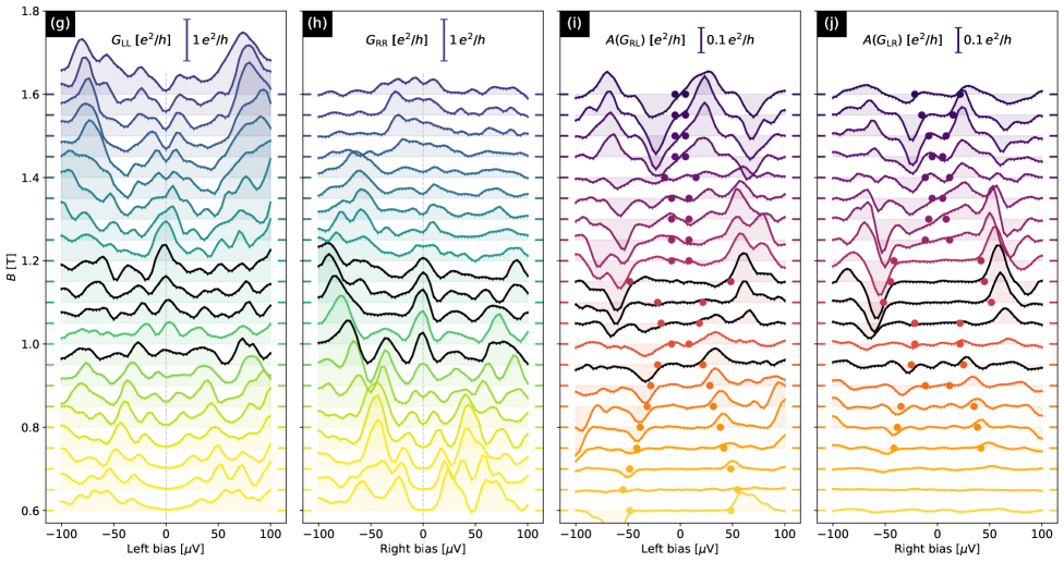
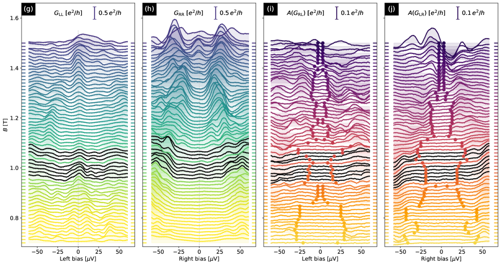
4.2.1 Device B passing TGP
Since device B has a considerably larger zero-field induced gap than device A, a topological phase would have to occur at higher magnetic fields. The TGP finds an experimental phase diagram that is consistent with this expectation. There is a topological phase transition at T, as shown in Fig. 15(a,b). The TGP assigns this device a maximum topological gap . The median value of the topological gap across the orange region in Fig. 15(a) is . Device B has , which is smaller than that of the other devices reported in this paper. This is consistent with device B’s large ratio, which implies that electrons in the lowest occupied sub-band have a higher amplitude to be in the superconductor, thereby inheriting both a larger induced gap and a smaller .
The extent of the SOI2 is T. The measured extent in is mV, however, Stage 2 did not go to lower than V, where the SOI2 still appears to be quite robust, so it is possible that this underestimates the size of the SOI2. It is also possible that the blue region centered around T and V — which the TGP identifies as a gapped trivial region due to the absence of stable ZBPs — is actually topological but has MZMs that are poorly coupled to the leads. There are some sign changes in the non-local conductance, such as the one that occurs at T in Fig. 15(e,f). Since and are suppressed at these sign changes, they lead to large values of the extracted gap, which can bias towards larger values. However, even the median gap is , and there is a clearly identifiable gap edge at in at T. “Waterfall” plots for local and non-local conductances at fixed plunger V are shown in Fig. 15(g,j). Additionally, in Fig. 16 we show “waterfall” plots of conductances for fixed magnetic field T corresponding to the vertical line in Fig. 15(b).
As noted above, device B has the largest value and the smallest value reported in this paper and, perhaps not surprisingly, the largest topological gap as well. The topological gap is actually equal, within error bars, to the largest topological gap that we would expect for a perfectly clean, infinitely-long DLG- device. This is not a contradiction. Finite-size effects can increase the gap. We measure a transport gap, which is the gap to extended states (for ), and it can be larger than the gap in the spectrum if states at the gap edge have short localization lengths.
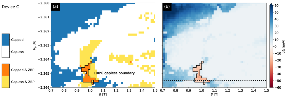
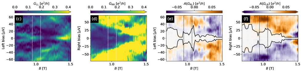
4.2.2 Devices C and D passing TGP
The experimental phase diagram for device C is shown in Fig. 17. The TGP assigns this device a maximum topological gap , which is comparable to that of A1 and A3. The lowest field at which the gap closes is T, corresponding to , which is comparable to but smaller than that of device A. The extent of the topological phase is mV and T. On the other hand, device C’s ROI2 is at significantly lower plunger gate voltage V than device A’s. We attribute this to differences in the dielectric that that are evident from Hall bar measurements. In addition, the gap closing in device C is more clearly visible in than in , and the ZBP has much higher amplitude in than in . The data is otherwise similar to that obtained from device A.
In Fig. 18, we show data from device D. There are two topological regions in the phase diagram. The TGP assigns maximum topological gaps of for the top and bottom regions, respectively. Even taken together, these regions occupy relatively small fraction of the phase diagram. The top cluster is detected at T whereas the bottom one appears at T. The latter is a relatively high field, but it is consistent with the broad distribution of fields that we find in simulations.
Our results on device D show that the TGP can even identify small ROI2s with small topological gaps.
4.2.3 Devices E and F not passing TGP
In Fig. 19, we show data from device E. This device has large regions with stable ZBPs at each end and thus shows a relatively large ROI1 in the Stage 1 of the TGP. However, in Stage 2 the system appears gapless throughout the region of interest: The induced gap closes and there are no signatures of gap re-opening in the non-local measurements. Since the system appears gapless in non-local conductances it is unclear if the correlated ZBPs correspond to a topological or trivial phase — either the topological gap is too small to be experimentally resolved or we observe a trivial state that couples to both sides because of the long coherence length that is expected in a system with very small gap. The fact that the ZBP is significantly brighter in than in as well as the similarity of finite-bias features in local measurements hints towards the second scenario. In both cases, such a phase would not be suitable for topological quantum computation. This example demonstrates the importance of Stage 2 of the TGP where non-local conductance is measured in order to identify false positives from Stage 1.
Meanwhile, device F does not have any regions with stable ZBPs at both ends, as may be seen in Fig. 20. The absence of correlations may be due to an inhomogeneous slowly-varying potential along the nanowire. The ZBPs that are seen at one end or the other are very similar to the ZBPs that are seen in devices passing the TGP. However, the ZBP that show up in more than 70% of cutter settings show no stable correlations between the two junctions. They may originate from a trivial Andreev bound states (ABS) crossing zero energy or stable ZBPs, dubbed quasi-MZMs, that appear due to a slowly-varying potential near the junction. Such states do not span over the whole length of the wire. The absence of a large enough cluster of correlated ZBPs causes this device to fail Stage 1 of the TGP.
5 Summary and discussion
In the previous sections, we have presented a summary of observed phenomena in gate-defined semiconductor nanowires coupled to a superconductor. We have demonstrated that, when devices A-D are tuned to the single sub-band regime, they yield data passing the TGP at magnetic fields in the range -T. We have observed topological gaps as high as . We emphasize that our results are reproducible within the same cooldown and between different cooldowns, as we have shown for device A. In short, our main empirical result is that multiple devices have passed the TGP.
These measurements represent strong evidence for the observation of a topological superconducting phase supporting MZMs. The TGP has been tested with extensive simulations, reliably identifying topological regions of the phase diagram of simulated devices and correctly distinguishing trivial Andreev bound states from Majorana zero modes. We found that, for a simulated device, there is probability that, when the TGP finds an ROI2, there is a topological phase in this region of its phase diagram.
| Device, measurement | Design, stack | GB | |||||
| A, A1 | SLG- | 23 | 5.6 | 0.5 | 12 | 1.7 | 78 |
| A, A2 | SLG- | 29 | 6.4 | 0.5 | 8.6 | 1.0 | 80 |
| A, A3 | SLG- | 22 | 6.4 | 0.2 | 5.7 | 1.0 | 90 |
| B | DLG- | 61 | 3.7 | 0.2 | 0.3 | 2.1 | 92 |
| C | DLG- | 19 | 4.4 | 0.1 | 2.0 | 1.0 | 100 |
| D | DLG- | 17 | 4.5 | 0.1 | 2.5 | 1.8 | 100 |
| D | DLG- | 21 | 4.5 | 0.1 | 1.4 | 1.1 | 93 |
In order to guide incremental progress towards passing the TGP, we relied on our estimates of the material and disorder requirements that gate-defined nanowires must satisfy. We developed designs and fabrication processes capable of meeting these requirements.
In the remainder of this section, we turn to the interpretation of our results. The stability of the identified topological phase as a function of and is an important consistency check for our results. For the extracted effective -factor in measurement A1, mT corresponds to a Zeeman energy of and, for the calculated lever arm of meV/V, mV corresponds to a chemical potential shift of , see Eq. 1. In other words, the phase space extent in field is times and the extent in gate voltage is times the maximum topological gap of . In measurement A2, we found that the topological region in Fig. 12 extends over a maximum -field range mT and a maximum mV, corresponding, respectively, to energy scales of and . The other devices/measurements have similar stability in and . Since the topological phase has an irregular shape, its area is smaller than the product of and ; it is listed in Sec. 5, where the areas of the other measured topological regions is also listed. All of the devices have in the range 0.1-0.5 mVT, and they have values that are larger than — in some cases, substantially larger — except device B. Note, however, that device B may have a larger SOI2 than what we can see in Fig. 15, extending below V. In other words, the observed candidate MZMs are stable with respect to parameter changes comparable to or larger than the maximum topological gap, which is an intrinsic energy scale of the problem that was determined from non-local conductance measurements.
The summary of the simulated data in the magnetic field range , which is comparable to experiment, is shown in Sec. 5. Here we present a brief summary; the raw data set is available [96]. The TGP yield and the average volume of SOI2 decreases with disorder strength (leaving aside the case of which requires a different TGP calibration). The observed phase space of the topological phase is consistent with the results of simulations presented in Sec. 5, where we found that simulated SLG- and DLG- devices had mean in the range 0.1-mVT, but with a distribution that has long tails extending up to large volumes. Similarly, our simulated SLG- devices have values in the range 23- while our simulated DLG- devices have values in the range 25-, both with long tails at large gaps. Device A would appear to be in the tail of the distribution, both with respect to and while device B appears to be in the tail of the distribution with respect to . In summary, the phase space for the topological phase is roughly as large as we would expect for a maximum topological gap of 20- and broadly consistent with our simulations. We note that this is a larger gap than in early measurements of the fractional quantum Hall state [106, 107] and further note that the topological gap at subsequently increased dramatically with material quality [108, 109].
The measured , , values in Sec. 5 are consistent with the simulated values in Sec. 5, which further validates the simulation model that was used to estimate the FDR. The primary outliers are for measurements A1 and A2 and for device B; they are substantially larger than the mean values in simulations, but within the long tails of the non-Gaussian distributions found in simulations (see Appendix D for details). This consistency between simulated and measured values validates the model used to test the TGP, as suggested in Ref. 104.
| Design, stack | Yield T | ||||
| SLG- | 1.0 | 23 | 0.2 | 1.9 | |
| 2.7 | 34 | 0.1 | 1.5 | ||
| 4.0 | 34 | 0.1 | 1.5 | ||
| DLG- | 0.1 | 35 | 0.2 | 2.2 | |
| 1.0 | 29 | 0.2 | 2.3 | ||
| 2.7 | 30 | 0.2 | 2.2 | ||
| 4.0 | 30 | 0.1 | 2.2 |
We now consider other potential explanations of our results. According to our simulations, the probability that a device that passes the TGP does not have a topological phase overlapping the ROI2 is less than 10%, so any other explanation is extremely unlikely, though not impossible. For an intuitive understanding of why other explanations are unlikely, let us discuss trivial ZBPs. First, we observe that all of our devices have trivial ZBPs, even the ones that pass the TGP. Often, they occur at only one junction, but they sometimes occur at both junctions and they can even be stable to changes in junction transparency and also to changes in and . For instance, there are stable ZBPs at both junctions in measurement A1 for T and V, as may be seen in Fig. 10. In device E, there are stable ZBPs at both junctions for T and V, as may be seen in Fig. 18. These are all trivial and fall outside the topological region because the observed bulk transport gap is zero.
Now, let us consider the causes of trivial ZBPs. One possible origin is a slowly-varying potential near the end of a device, which can be caused by certain tunnel barriers. In sufficiently clean devices, this can lead to quasi-MZMs before a bulk gap closing, where they are a precursor to the topological phase transition [46, 47, 48, 49, 51]. Quasi-MZMs do not appear after a gap closing/re-opening. If the bulk gap never re-opens, as in Fig. 28(g-j), then quasi-MZMs fail to become MZMs. However, if the bulk gap re-opens, as in Fig. 28(c-f), then quasi-MZMs evolve into true MZMs. By design, Stage 2 of the TGP weeds out stable ZBP clusters in which quasi-MZMs don’t evolve into true MZMs.
Trivial ZBPs can also be induced by disorder in proximitized semiconductor nanowires with spin-orbit coupling [43, 44, 45]. However, this scenario does not entail a gap closing and re-opening in the non-local signal, from which we conclude that it does not apply to devices A, B, C, and D. ZBPs can also be caused by trivial ABS, which can “accidentally” pass through zero energy. It is very difficult to discern a trivial ABS from an MZM purely from the local conductance spectroscopy, which can be virtually identical. However, as in the case of disorder-induced ZBPs, a trivial ABS need not be accompanied by a gap closing and re-opening in the non-local signal.
A gap closing/re-opening could be caused by the orbital effects of the magnetic field. When half a flux quantum is threaded through the effective cross-sectional area of the device, the proximity effect is suppressed, and the gap closes. It re-opens when the flux increases still further, closing a second time when flux quanta thread the active region. For device A, we expect a gap closing due to orbital effects at T in higher sub-bands and even higher fields T in the lowest sub-band. The observed gap closing is at much lower fields. Crucially, a gap closing due to orbital effects would be weakly-dependent on the gate voltage, as illustrated by the simulated phase diagrams of clean systems in Fig. 4, where the first closing due to orbital effects is a wide, nearly vertical white bar at T that intersects the topological lobes at V and V (SLG-) or V (DLG-). We find similar behavior in the simulations that we used to test the TGP, which include disorder. On the other hand, as may be seen in Fig. 12, the gap closing that is observed in measurement A2 is strongly dependent on the gate voltage: at V, the gap closes at T, but at V, it is still open at T. Similarly, device C has a gap closing that occurs at T at but it is still open at T at . Devices B and D have ROI2s that occur at higher fields, but still below T, and the gap closings are at, respectively, T and T. To determine the dependence of the gap closing in device B, we performed a large scale Stage 1 scan, which shows clear dependence, with a trivial gap that that is still open at T for some values of . Hence, an explanation relying on the orbital effect of the magnetic field is not consistent with either the field value or the -dependence of the observed gap closings/re-openings in devices A-D.
Of course, it is conceivable that the bulk gap closes and re-opens accidentally and that trivial ZBPs also accidentally occur for the same and . But to pass the TGP, the accidental closing would have to occur over an entire curve in the - phase space and, moreover, the trivial ZBPs would have to persist over the enclosed region. Of course, we cannot rule this out completely. However, such coincidences do not require any physics that is not incorporated in our simulations. Hence, they could occur in our simulations, and we can quantitatively bound their probability. The false discovery rate (FDR) that we estimate from simulations is at a 95% confidence level for all of the device designs, material stacks, and disorder levels that we have simulated, which implies that there is a low probability that data from devices A-D can be explained by trivial ZBPs that occur coincidentally with an accidental gap closing/re-opening instead of a topological phase.
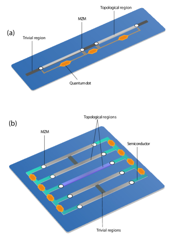
6 Looking ahead
A reliable process for tuning devices into the topological phase is an essential step on the journey to topological quantum computation, which relies on the fusion and braiding of anyons. Networks of such wires can be assembled into a many-qubit device, and this protocol can be used to tune each wire within a qubit into the topological phase. The linear tetron qubit [110, 111] is a minimal device for performing two non-commuting fusion operations;666See Refs. 112, 113, 114, 115, 116 for related alternate qubit designs. it is shown schematically in Fig. 21(a). There are two outer topological sections, separated by a trivial section. Fusion outcomes for different pairs of MZMs are measured by coupling these MZMs to adjacent quantum dots. By measuring different sequences of pairs of MZMs, we can directly measure the fusion rules, a topological invariant of the state. The parameter space of such a device is simply too large to explore in the hope of finding a suitable operating point unless each of the outer sections of the nanowire is individually tuned into a topological phase, which can be achieved using the TGP.
Coherent manipulation of the encoded quantum state, for example through measurement-based implementations of braiding transformations [117, 118], requires an even more complex device, as shown in Fig. 21(b). This device consists of two superconducting islands, each comprised of two topological segments linked together by a short region of trivial superconductor, and thus contains two qubits. We refer to this configuration as a two-sided tetron because MZMs are on each side of the device. The additional topological wire between the qubit islands, shown in purple, is added to allow measurements between MZMs on opposite sides of the islands. In this device, unitary Clifford gates on one of the two qubits can be performed by using the other as an auxiliary qubit and performing a sequence of single- and two-qubit measurements [111]. Despite the even larger parameter space, these devices can be tuned using the TGP. Continued improvement in simulation, growth, fabrication, and measurement capabilities will be required to achieve the topological gap required for such coherent operations.
Acknowledgements.
We thank Greg Boebinger, Sankar Das Sarma, Michel Devoret, Klaus Ensslin, Leonid Glazman, Bert Halperin, Dale van Harlingen, Kam Moler, Krysta Svore, and Matthias Troyer for extensive discussions. We are grateful to Edward Lee and Todd Ingalls for their assistance with figures. We thank Leo Kouwenhoven for helpful comments on a previous version of this manuscript. Correspondence and requests for materials should be addressed to Chetan Nayak (cnayak@microsoft.com). †Morteza Aghaee, Arun Akkala, Zulfi Alam, Rizwan Ali, Alejandro Alcaraz Ramirez, Mariusz Andrzejczuk, Andrey E. Antipov, Pavel Aseev, Mikhail Astafev, Bela Bauer, Jonathan Becker, Srini Boddapati, Frenk Boekhout, Jouri Bommer, Esben Bork Hansen, Tom Bosma, Leo Bourdet, Samuel Boutin, Philippe Caroff, Lucas Casparis, Maja Cassidy, Sohail Chatoor, Anna Wulf Christensen, Noah Clay, William S. Cole, Fabiano Corsetti, Ajuan Cui, Paschalis Dalampiras, Anand Dokania, Gijs de Lange, Michiel de Moor, Juan Carlos Estrada Saldaña, Saeed Fallahi, Zahra Heidarnia Fathabad, John Gamble, Geoff Gardner, Deshan Govender, Flavio Griggio, Ruben Grigoryan, Sergei Gronin, Jan Gukelberger, Sebastian Heedt, Jesús Herranz Zamorano, Samantha Ho, Ulrik Laurens Holgaard, William Hvidtfelt Padkær Nielsen, Henrik Ingerslev, Linda Johansson, Jeffrey Jones, Ray Kallaher, Farhad Karimi, Torsten Karzig, Cameron King, Maren Elisabeth Kloster, Christina Knapp, Dariusz Kocon, Jonne Koski, Pasi Kostamo, Peter Krogstrup, Mahesh Kumar, Tom Laeven, Thorvald Larsen, Kongyi Li, Tyler Lindemann, Julie Love, Roman Lutchyn, Michael Manfra, Elvedin Memisevic, Trevor Morgan, Chetan Nayak, Bas Nijholt, Morten Hannibal Madsen, Signe Markussen, Esteban Martinez, Robert McNeil, Andrew Mullally, Jens Nielsen, Anne Nurmohamed, Eoin O’Farrell, Keita Otani, Sebastian Pauka, Karl Petersson, Luca Petit, Dima Pikulin, Frank Preiss, Marina Quintero Perez, Katrine Rasmussen, Mohana Rajpalke, Davydas Razmadze, Outi Reentila, David Reilly, Richard Rouse, Ivan A. Sadovskyy, Lauri Sainiemi, Sydney Schreppler, Vadim Sidorkin, Amrita Singh, Shilpi Singh, Sarat Sinha, Patrick Sohr, Tomaš Stankevič, Lieuwe Stek, Henri Suominen, Judith Suter, Vicky Svidenko, Sam Teicher, Mine Temuerhan, Nivetha Thiyagarajah, Raj Tholapi, Mason Thomas, Emily Toomey, Shivendra Upadhyay, Ivan Urban, Saulius Vaitiekėnas, Kevin Van Hoogdalem, Dmitrii V. Viazmitinov, Steven Waddy, David Van Woerkom, Dominik Vogel, John Watson, Joseph Weston, Georg W. Winkler, Chung Kai Yang, Sean Yau, Daniel Yi, Emrah Yucelen, Alex Webster, Roland Zeisel, Ruichen Zhao.Appendix A Effects of disorder
A.1 Projection to proximitized nanowire model
The disorder-free limit of the single-sub-band regime is well-represented by a Hamiltonian of the form of Eq. 1:
| (5) |
In Eq. 5, the effective mass, -factor, and spin-orbit coupling in — obtained by projecting the full model for the device designs and material stacks described in Secs. 2.2 and 2.3 into the lowest sub-band — take the values given in Sec. 2.4. The parameters in Sec. 2.4 are weakly density-dependent, so they were computed at , which corresponds to a Fermi wavelength in range -80 nm. Compared to Eq. 1, there is a transformation , described below, which is due to the renormalization of the electrons in the semiconductor by their coupling to the Al, which has a superconducting gap and a Zeeman potential with -factor .777Note that this effective Hamiltonian is only valid provided is not too small. In the more general case, integrating out the superconductor leads to an effective action that is non-local in time and has an energy-dependent renormalization. In the following we will neglect the orbital effect of the magnetic field on the superconductor, despite keeping the Zeeman splitting. The justification for this is that the SC thickness is nm and we estimate the disordered coherence length in the Al, , to be around nm. Orbital effects can be neglected when the depairing energy is small compared to the gap; this ratio goes as the square of the ratio of flux through the effective cross-section to the flux quantum, yielding a condition [119]. For fields T, the left hand side is less than , so we expect the corrections due to orbital effects to be correspondingly small. The effective pairing depends on the Zeeman potential in the SC as . Additionally, the Zeeman potential experienced by the SM now includes an induced contribution from the Al, .
In all three cases — SLG -stack and DLG - and -stacks — the transformation by as well as the induced Zeeman energy from the Al suppress the effective -factor below . Hence, as discussed in the previous section, the coupling between the semiconductor and the superconductor, , should not be too large or else the -factor will be strongly suppressed and the topological phase will be pushed to high -fields where the Al approaches the Clogston limit. On the other hand, cannot be too small, either, or else the induced gap will be small.
We now turn to the renormalization factor . The Green’s function of a hybrid SM-SC system is given, in general, by
| (6) |
with a self-energy obtained by integrating out the SC degrees of freedom using the tunneling Hamiltonian model defined in Ref. 120,
| (7) |
Here, the integrals are taken over the superconducting domain with where and are out-of-plane and in the plane of the interface, respectively; the tunneling matrix elements element reads
| (8) |
The delta function here corresponds to momentum conservation parallel to the interface whereas enhances transmission for electrons in the superconductor that are incident with momemtum normal to the interface. After some algebra [27], one finds that where represents the rapid decay of the self-energy on the scale of the Fermi wavelength in the metal.
We now derive the expression for the self-energy in the presence of disorder in Al which is crucial for understanding the proximity effect [27, 121, 122, 123, 124]. Indeed, disorder removes momentum conservation constraints and effectively increases the tunneling rate . The disorder-averaged self-energy can be written as
| (9) |
where the Usadel Green’s function represents the diffusive limit of a spin-split s-wave superconductor. Here we neglect the orbital contribution of the magnetic field, as justified above. Analytic expressions for this Green’s function in this limit have been recently reported in Refs. [125, 126].
Now, we would like to obtain a frequency-independent effective Hamiltonian with eigenvalues that approximate the poles of (6), but, in order to do so, it is insufficient to take the static limit by replacing by . A better, widely used, approximation involves grouping the linear-in-frequency part of the self-energy, , with the frequency of the Green’s function to define an overall renormalization of the energy scale before taking the static limit. Here we describe a generalization of that method.
| (10) |
| (11) |
and the Green’s function in this linearized representation is
| (12) |
As a consistency check, we can consider the well-known limit, where and and recover
| (13) |
with poles at the eigenvalues of the renormalized effective Hamiltonian
| (14) |
recovering the previous results of Ref. [27]. In the more general case where , is not proportional to the identity. Hence, we have to be careful in factoring out the coefficient of . This is because we require a hermitian , and in general the matrix is not hermitian. To resolve this, we take a symmetric product, defining and obtain the result
| (15) |
Finally, we now extend the model to include potential disorder in the semiconductor:
| (16) |
where the disorder potential, projected into the lowest subband, is
| (17) |
For the disorder mechanisms we have included, we find that the random potential can be approximately characterized by its sample-averaged autocorrelation:
| (18) |
The projected disorder parameters, variance and correlation length , 115, and 120 nm (for -, -, and -stacks, respectively), are obtained for the same design and materials stack as the uniform parameters given in Sec. 2.4. Here, the various sources of disorder and their strengths have been distilled to two numbers. These parameters’ relation to the underlying microscopic disorder depends on both the device geometry and the defect types and densities. We show the relation between and for SLG and DLG designs for the , , and stacks in Fig. 22.
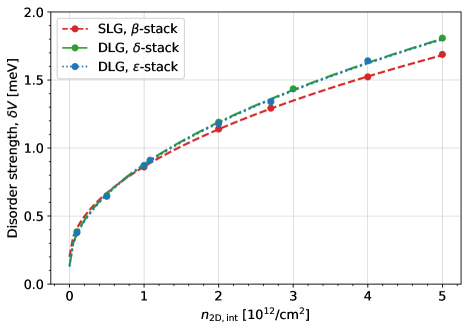
A.2 Disorder-driven phase transition
In general, disorder suppresses the topological phase [127, 128, 129, 130, 131, 132, 133, 134, 135, 136, 137], causing important changes to the phase diagram of Fig. 1. For weak disorder, this leads to a decrease of the topological gap and an increase of the disordered superconducting coherence length in the topological phase. As the disorder strength is increased, these variations can create small non-topological regions in an otherwise topological wire, thus nucleating additional subgap states at the domain walls between topological and non-topological regions. Eventually, these subgap states hybridize and lead to the breakdown of the topological phase through Griffiths’ effects [127]. In the limit in which the clean topological gap is small compared to the Fermi energy, the stability condition for the topological phase is [130], where is the localization length in the normal state (which in one dimension and for short-ranged disorder is equal to twice the mean free path [138]) and is the coherence length in the clean topological superconductor. Equivalently, this can be rephrased in terms of energy scales as , where is the elastic scattering time. In the effective model governed by , the scattering rate due to the random potential can be evaluated to lowest order in :
| (19) |
Here, and are the Fermi energy and momentum. Thus, the transition at occurs at a critical value :
| (20) |
This expression for the critical disorder strength is valid in the regime of weak disorder and small gap, . However, the nanowire in the single subband regime has a small Fermi energy, so the latter requirement is difficult to satisfy. Moreover, disorder sources with correlation lengths cause stronger scattering than short-range disorder , as may be seen from Eq. 19. For realistic disorder levels, it is necessary to go beyond lowest-order in [101]. Consequently, the precise location of the disorder-driven phase transition is more complicated than Eq. 20 when the clean topological gap and disorder strength are comparable to the Fermi energy [133, 101]. Finally, there are important differences between the thermodynamic limit and finite-sized systems, where the phase transition is rounded into a crossover. In order to understand these additional complexities, we calculate the disordered coherence length numerically using the transfer matrix method, as we discuss in the next two subsections.
A.3 Length scales and topological phases in finite systems
Since we are concerned in this paper with topological phases in finite systems with disorder, we must pay attention to several important length scales. We will denote the superconducting coherence length in the wire by . It is the distance that a zero-energy unpaired electron can penetrate into the proximitized nanowire. In the topological phase, corresponds to the localization length of a Majorana zero mode. The coherence length diverges at the phase transition between the trivial and topological superconducting phases. In the topological phase, when disorder is very weak, approaches its clean value . Increased disorder elongates in the topological phase, while it shortens in the trivial phase.
In a perfectly clean system, there would be no states below the clean topological gap , apart from the MZMs, and states above the gap would all be extended. However, even weak disorder localizes all states except the zero-energy state at the critical point, as noted in Sec. 2.1. It also causes localized states to appear below . We will call the energy-dependent localization length, calculated for the Bogoliubov-de Gennes Hamiltonian (1), . At low energy, . When disorder is very weak, the density of states is very low for , and these states have localization lengths that grow smoothly as a function of , increasing from to . At energies , the localization length is proportional to the mean-free-path . If , then states above will appear to be extended and there will be an apparent transport gap , which is the gap to “extended states,” namely the states whose localization lengths are larger than the system size. Turning now to the case of more general disorder strengths, we define as the maximum value of for . Our devices are designed so that . When this holds, we can measure the transport gap , which is the minimum for which is small enough that states at energy are visible in bulk transport. We explain these measurements in Sec. 3 and Sec. C.1.
The decay of subgap states at small energies is controlled by while transport by excited states is controlled by . Hence, if we observe a ZBP at one junction, the amplitude to observe it at the other junction decays as , but if we observe an excited state of the bulk at one junction, the amplitude to observe the same state at the other junction decays at least as fast as .
Thus, depending on the disorder level and device length, there are three parameter regimes for the operation of a topological device. The first regime is when . In this limit, the device is longer than any of the finite length scales that characterize the topological phase. Hence, there is no characteristic energy scale of the bulk topological phase that can be extracted from transport measurements.
In the second regime, . In this regime, which we will call the asymptotic regime, the device is much longer than the localization length of a low-energy bound state. When ZBPs are observed at both junctions, we know that there are two distinct bound states, one at each junction. Since , there are excited states that are effectively extended, i.e. have localization lengths that are comparable to or longer than the system size. The transport gap is the energy gap to such states.
Finally, there is a third regime, in which . This is a crossover regime in which the system is longer than the MZM localization length but it may not be so much longer that we are in the asymptotic limit. In this case, there may be some bulk transport at zero energy even when because the contribution is not negligible. Consequently, the system will be intermediate between the asymptotic regime and the critical regime that we define in the next paragraph. As is reduced, the system will move more firmly into the asymptotic topological regime. However, there isn’t a particular value of the ratio that separates the crossover regime from the asymptotic regime; the evolution from one to the other with increasing is smooth.
None of the three regimes mentioned above — thermodynamic, asymptotic, and crossover — is possible near the critical point, where . When , the system is in the critical regime, and we can’t distinguish it from a critical system. Even in a device of length , this is a fairly broad region. As we shall see, for intermediate disorder strengths, over much of the parameter range in which the system would be in the topological phase for , the system is in the critical regime because the correlation length is long and .
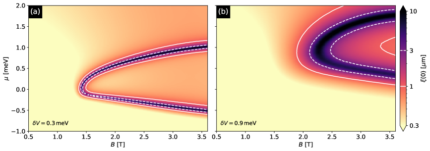
As an illustration of these various regimes, we calculate for the model Eq. 16 using the transfer matrix method [139]. In Fig. 23 we plot the result for DLG, -stack parameters from Sec. 2.4 and characteristic disorder strengths and meV. As is a function of the chemical potential and applied magnetic field, a finite wire can go from the critical to crossover to asymptotic regimes depending on these parameters. When the system is in the thermodynamic, asymptotic, or crossover regimes, it is deep in a phase. The devices discussed in this paper are in the asymptotic or crossover regimes. We discuss the implications for transport measurements when we described the topological gap protocol in Sec. 3 and Sec. C.1.
A.4 Finite-size behavior of topological invariants
We now consider the finite-size behavior of the invariants distinguishing the topological and trivial phases. We consider the “scattering invariant” [103] and the Pfaffian invariant [9, 97]). The scattering invariant is defined for an open system with a junction to a normal lead: , where is the reflection matrix. When , there is an MZM at the junction. The scattering matrix depends on how open or closed the junction is. In a finite-sized system, an MZM at a junction will hybridize with the MZM at the other end of the wire with strength (giving ) unless it is coupled more strongly to the lead. If the MZM couples poorly to the leads, then we will erroneously find . If the MZM couples more strongly to the lead than to its partner at the other end, then we will have in a finite-size system. Note, however, that we will also find if the second MZM is much closer than distance but has small hybridization with the one at the junction, namely the “quasi-MZM” scenario [46, 47, 48, 49, 51]. The Pfaffian invariant is defined for a closed system as the relative sign of the ground state parity between periodic (PBC) and anti-periodic (APBC) boundary conditions. when the Bogoliubov-de Gennes Hamiltonian is written in terms of real fermionic operators , so that it takes the form . In a finite system, we will have when the hybridization of the two MZMs is larger via the periodic boundary condition that connects the two ends than the hybridization that occurs through the bulk of the wire. In summary, both invariants rely on being smaller than the coupling to the lead or the boundary condition. This is the limit in which the topological phase can be defined; it becomes more clearly distinct from the trivial phase in a continuous fashion as . In the next section, we will use the Pfaffian invariant to illustrate the combination of finite-size effects and disorder on the phase diagram. In Sec. D.3, we will use the scattering invariant to test the accuracy of the TGP because the scattering invariant can be calculated for the same device geometry and junction settings as used in transport simulations and measurements.
Appendix B Electrostatic calibration from Hall bars
Each of the topological gap devices described in the main text is accompanied by a Hall bar device subject to the same growth and fabrication processes; this Hall bar enables a characterization of the bulk material quality. The full density dependence of the Hall mobility has been widely used previously to identify and quantify dominant scattering mechanisms in 2DEGs [140, 141, 142, 143, 144, 145, 146, 147, 148, 137]. In particular, across all samples, the low-density mobility rapidly increases with increasing density, consistent with the mobility being dominated there by scattering from the long-range Coulomb potential of remote impurities.
In our simulations, we calculate (i) the gate-voltage dependence of carrier density for a 2DEG in our materials stack in a standard Schrödinger-Poisson framework; and (ii) the remote-impurity-limited mobility in the Boltzmann-Born formalism. Both of these functions are parameterized by the density and location of impurities, and an effective composite dielectric permittivity. These parameters are used to simultaneously fit the model traces to experimental data. As mentioned in the main text, our best fits to density and mobility measurements over a variety of samples suggested a simplification in which an effective 2D impurity density is placed in an “impurity layer” at the interface between the barrier and the gate dielectric. Small changes in the position or width of the impurity layer can be compensated by tuning the impurity density, but large changes modify the overall density dependence of the mobility and result in poor fits. Therefore, the values of charge impurity density that we quote here depend on the disorder model employed, with the goal of this model being to provide a consistent description of the impact of fixed charges on both the Hall mobility and TGP measurements.
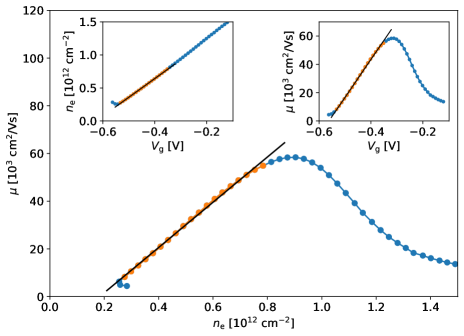
Figure 24 shows a representative example measurement of mobility versus density for the Hall bar proximate to device A [note that the low-density upturn in and non-single-valued arise due to a measurement artifact and these points are excluded from the fitting]. The solid black lines represent our point estimate traces corresponding to the most-probable values of the effective impurity density, , and effective dielectric permittivity.
Using similar analysis, we extracted the corresponding effective charged impurity densities at the interface with the dielectric for devices C-F yielding , , , and , respectively.
Appendix C TGP: Subtleties
C.1 TGP measurements
First, to accelerate the search for ZBPs in Stage 1, rather then doing lengthy bias-voltage sweeps, we employ the third-harmonic () technique described in Ref. 149. This gives a direct measurement of , which is the curvature of the local conductance . When is negative and above the noise level, it indicates the presence of a ZBP. Using this technique, we are able to scan over a large area in phase space by varying four parameters: , and the two cutter gate voltages , that modulate the junction transparencies. We further facilitate this by restricting the cutter gate voltages so that at each junction is limited to the range - as a compromise between sufficient visibility and remaining in the tunneling regime. In Stage 2, we will also sweep , but will restrict to smaller ranges.
Second, and may receive contributions from line impedances in the measurement circuit, which we account for by taking the full impedance network into account [150]. In addition, we correct for finite frequency effects by calibrating the resistances and capacitances in the measurement circuit, as explained in Appendix E. Finally, we remove any remaining voltage divider corrections and improve SNR by focusing on the parts of the non-local conductances that are antisymmetric in bias voltage, , :
| (21) |
and similarly for . A discussion of relevant multi-terminal conductance symmetry relations may be found in Ref. [151].
Third, the transport gap extracted from will not, in general, be the same as that extracted from . The underlying transport gap is the same, but the two non-local conductances may not be the same due to the different ways in which local matrix elements enter and . [We will see an example of this in simulated data in Fig. 26(b,c) in Sec. D.3.] This can obscure a gap narrowing or closing. Hence, for any given and , we determine the induced gap as the lower of the gaps extracted from and . Consequently, the observation of non-vanishing or at bias voltages approaching zero is a signature of a bulk gap closing. Note that the energy spectrum can be gapless due to the presence of disorder-induced localized states at low energies. The observed transport gap, extracted from and , is the gap that we really care about since it is more predictive of qubit performance.
A fourth subtlety is that can be either positive or negative, depending on whether transport at that bias voltage is primarily due to electrons or holes. It can change sign as the matrix elements change as a function of or , passing through zero when this occurs [102]. Such a sign change can appear as a very sharp increase in the induced gap, centered about some or value. In determining the zero-field induced gap, we simply avoid these points. The situation is slightly more complicated for the topological gap, since it varies between zero at the phase transition and a maximum value that determines the stability of the topological phase. Hence, we will report both the median value of the gap over the SOI2 and also its maximum value. However, we will not extract the maximum from the single point at which it is largest. It is not uncommon to have a very small region over which the extracted topological gap is very large because one of the aforementioned sign changes occurs, suppressing the signal in and . Hence, we define the “maximum topological gap” to be the upper quintile of measured gap values within SOI2.
We add a note of caution here that the measured values of and are transport gaps, which are the lowest energy at which there is an excited state whose localization length is longer than the device length; they can be larger than the or expected for a clean system.
Fifth, we clarify the definition of the gapless boundary of an SOI2. The boundary of the region is defined to consist of all points inside the SOI2 that neighbor the exterior of the SOI2 on the side or diagonally. Each such boundary point is then considered gapped if all of the neighboring points outside SOI2 are gapped. Otherwise the boundary point is considered gapless. Using this definition, we extract the fraction of the boundary points that are gapless.
C.2 TGP parameters
The TGP is parametrized by thresholds that were fixed by an initial set of calibration simulations described in Sec. D.2 and then tested extensively by large-scale simulations for different disorder levels and device designs, as described in Sec. D.1. As a result, we have high confidence that ROI2s overlap with the regions in parameter space where there is a topological phase, as we quantify in Sec. D.1.
In principle, this protocol is designed to detect any topological phase with a sizable gap. Finite experimental resolution and temperature, however, may obfuscate some of the topological signatures, giving rise to subtleties when interpreting the data that we discuss here.
A wire may have MZMs, but one or both of them may be slightly displaced from the end of the wire for some choices of junction transparency and, therefore, may not be visible. (Indeed, we see in Fig. 2(c) that the local density of states can be peaked a few hundred nanometers away from the junction in a simulation of an ideal disorder-free device.) For this reason, we do not insist that a ZBP be present for all junction configurations and, instead, consider a ZBP to be stable in Stage 1 if it is visible for at least 70%, of measured junction transparencies. We define the “cutter gate fraction” as the fraction of junction transparencies (or, equivalently, cutter gate settings) for which a ZBP is present. For instance, suppose we pick cutter gate voltages at the right junction such that at the right junction takes the values 0.35, 0.49, 0.62, 0.76, and similarly pick cutter gate voltages at the left junction so that at the left junction ranges over the same five values. Then, a -point will be said to exhibit stable ZBPs at both junctions if there are ZBPs at both junctions for of cutter gate pairs .
For Stage 2, we set a threshold percentage and define a stable ZBP as one that is visible for at least of junction transparencies. As we discuss further in Sec. D.2, we use calibration simulations to inform the choice for the device parameters considered in this paper. For the junction transparencies given as an example in the previous paragraph, we would perform Stage 2 measurements for 5 different cutter gate pairs such that , 0.49, 0.62, 0.76, . A stable ZBP in Stage 2 would then need to be present for 3/5 cutter gate pairs.
A gap closing may not be visible even when it is present because and tend to be small at low bias voltage (due to their anti-symmetry in bias voltage) and will be suppressed even further by disorder and non-uniformity. Another reason why an SOI2 may be gapless along less than 100% of its boundary is that neighboring gapped regions may have been misidentified as non-topological (e.g. due to weak coupling of the MZMs to the leads or ZBP splitting due to a small topological gap). In case of such misidentification, such regions should actually be included in the SOI2, which would be larger and gapless along its entire boundary. To account for both of these possibilities, we set a threshold percentage . In order to qualify as an SOI2, a cluster must be gapless along at least of its boundary. As we discuss in Sec. D.2, we use simulated transport data to inform the choice for the device parameters discussed in this paper.
The non-local conductances and will never truly vanish at zero bias because there will at least be tunneling and thermally-activated contributions.888See also, Ref. 152 for additional considerations that are relevant to the non-local conductance. Hence, we need to give an operational definition for and . To do this, we define a threshold value . Then, if , , we interpret this as , . The extracted gap is obtained using the highest bias voltage below which and . The choice of should depend on and and also on the transparency of the junctions. For the disorder strengths expected in our devices, we take equal to times the maximal value of the non-local conductance at bias voltages greater than the induced gap (scanning over all for each for a given cutter configuration). As we discuss later in this section, this choice of was set by applying the TGP to calibration data from simulated devices with . For weaker disorder , the optimal value of should be smaller because and the transition becomes sharper in this limit. If we don’t take a smaller , the TGP will miss gap closings and will erroneously interpret and data as indicating that the gap remains open. Defining in terms of the high-bias conductance enables us to define it equally well for simulated data as for measured data (unlike, for instance, a that depends on the noise level in a particular measurement setup). When we plot either simulated or measured , we will use a black curve to indicate the bias voltage (as a function of field) below which each one is less than , see, e.g., Fig. 26(e,f). We can restate the threshold defined in this paragraph as follows: there is a truly sharp distinction between the trivial and topological phases only in the infinite-size, zero-temperature, and infinitesimal transparency limits; hence the threshold gives a simulation-tested method for finding the rounded transition.
Finally, we note that the extracted transport gap and, therefore, the phase diagram depend on the junction transparencies (and, thereby, on the cutter gate voltages that control them). The phase diagram must be stable to changes in the cutter gate voltages in the following sense: we require that a device passing the TGP must have a for a threshold percentage (see below) of cutter gate pairs . In other words, in order to pass the TGP, a fraction of cutter gate settings must have at least one that is a subset of the ROI2. We will take . This combination of the stability thresholds for ZBPs, gap closing and reopening requirements and the overlap of the resulting SOI2 is sufficient to virtually eliminate false positives when analyzing simulated data, as we shall see below in Sec. D.1.
Appendix D Calibrating and testing the TGP with data from simulated devices
In this section, we use simulations to quantify the reliability of the TGP. Our transport simulations begin with three-dimensional models of the devices in Figs. 2 and 3 that include the electrostatic environment defined by the set of gate voltages. We identify the range for which the chemical potential is in the lowest sub-band and the cutter gate voltages for which the junction transparencies take the values , 0.49, 0.62, 0.76, . The resulting single sub-band parameters are given in Sec. 2.4 and Fig. 22. For this gate voltage set, we perform transport simulations and calculate the scattering matrix of the system. The local and non-local conductances are then obtained by convolution with the derivative of the Fermi function at temperature . We analyze this data according to the TGP according to the same procedure that we will use in Sec. 4 to analyze experimental data.
D.1 False discovery rate
The basic question that we wish to answer is: suppose the TGP returns an ROI2 that passes; what is the probability that it does not have any overlap with the topological phase? The goal of TGP calibration is to set thresholds that minimize this probability. Once the TGP has been calibrated, we test it to assess whether this probability is low when the TGP is applied to a range of devices types and parameters: different junction designs, different material parameters such as spin-orbit coupling, different disorder strength.
To compute this probability in simulations, we compare ROI2s with a topological index (the “scattering invariant” [103]). We classify ROI2s as follows: if an ROI2 has any overlap with a region of the simulated phase diagram with scattering invariant , then we will call it a true positive; otherwise, it is a false positive. In Sec. 3 (see Eq. 4), we defined the classification of regions as TP and FP, and derived the FDR from these numbers in order to quantitatively measure the reliability of the TGP.
Note that this is a classification of regions, rather than a classification of devices. Hence, if a device that does have a topological region were to pass the TGP but its ROI2 were completely disjoint from the topological region, then this ROI2 would be a false positive. We do not attempt to count negative regions: an arbitrary region is very likely to be negative, so the number of negative regions is not a useful statistic.999On the other hand, a “negative device,” which is a device that fails the TGP, is a natural concept. We return to it later when we define the TGP yield, which is the probability that a device will pass the TGP — in other words, the complement of the probability of a negative device. Therefore, we do not compute the false positive rate (FPR), given by , where TN is the number of true negatives. The FPR is less useful for the present discussion.
There is a further subtlety, which is that the scattering invariant depends on the junction transparencies. Since our device has two junctions, the scattering invariant can be defined at either one: , where is the reflection matrix and , . When the junctions are completely closed, both are trivially equal to . When the junctions are opened, regions can appear, and they tend to grow as the junctions are opened further. Thus, we must decide how to assign a topological index to a finite system. We will define the topological region of the phase diagram as the union of the regions over , and the 5 different pairs of junction transparencies used in TGP Stage 2. We will call this union the “ region.” Instead of taking the union of the regions, we could have taken the intersections. In our simulations, and regions overlap but not completely. For some cutter gate settings, only while for others because a zero-energy state can couple poorly to the lead at one junction or the other for different cutter gate settings. Our definition of the topological index is relatively insensitive to these details of the junctions. If we had wanted to use the Pfaffian invariant [9], we would have had to truncate the system to remove the junctions and then imposed periodic/anti-periodic boundary conditions. This would no longer be the same device as we would be probing in transport.
A final technical detail: the conductance matrix is temperature dependent, and the output of the TGP has a resulting temperature dependence. As we discuss in Sec. 4, the base temperature of our dilution refrigerators during these measurements is mK, and the electron temperature is estimated to be mK. We use transport data at mK for our calibration simulations. We test the TGP using simulated data at mK, and we used this simulated data in our estimates of the FDR and other statistical properties.
The main result of the subsections that follow is that we estimate that the FDR is at a 95% confidence level for all device designs, material stacks, and disorder levels simulated. Thus, when a device passes the TGP, there is probability that it has a non-zero gap and . The details are in Sec. 3.
D.2 Setting the TGP thresholds
As discussed in Sec. C.2, there are three key thresholds which parametrize the TGP: , , and . We choose these parameters so that the TGP has a low FDR. If we were to make it very difficult to pass the TGP, then we would have very few false positives but also few true positives, and the FDR could be large. If we make it too easy to pass the TGP, then will have many more true positives but also more false positives. However, the right choices of , , and lead to a TGP which is reliable because it has low FDR.
We performed an initial calibration of the TGP by analyzing simulated transport data at mK from disorder realizations of an SLG- device with an average charged defect density of and spin-orbit interaction . We did not find any false positives: every ROI2 has at least some subset with . However, the number of true positives and, hence, the FDR varies with the threshold values. We find that , , and is close to optimal. There are 53 ROI2s spread across the devices (all true positives) for these threshold settings. Hence, the FDR is at the confidence level. Had and been set lower, we would have found ROI2s that did not contain a region with . For higher and , we would have had fewer devices passing the TGP. If we had set too low, then too much of the phase diagram would have been classified as gapless, thereby concealing gap re-openings. If we had set too high, then too much of the phase diagram would have been classified as gapped, obscuring gap closings. Note that the two thresholds, and are correlated.
We show two realizations of simulated SLG, -stack devices in Sec. D.5, one that passes the TGP and one that fails.
D.3 Testing the TGP
With the TGP thus calibrated and validated, we turn to simulations estimating the FDR. Since we will be analyzing experimental data from devices with different designs, material stacks, and disorder levels, we apply the TGP to simulated SLG- and DLG- devices with several different charge disorder levels. For charge disorder given by , we use the thresholds obtained in the calibration described above, whereas in the cleaner case of we lower from to while leaving the other thresholds unchanged. Although the optimal values of the thresholds in the TGP depend on the temperature, design, material stack, and disorder level, our goal here is to show that, for the thresholds chosen, the TGP remains reliable across a range of designs, material stacks, and disorder levels, and at a slightly higher temperature. The motivation is that we would like to apply the TGP in cases in which neither the electron temperature nor the disorder level is known precisely. Note, however, that if either the disorder level or temperature were very different, then we would probably need to adjust , , and .
To estimate the FDR, we performed large-scale simulations involving 349 different disorder realizations, distributed across SLG- and DLG- devices with intermediate to strong disorder levels defined by charge impurity densities of 0.1, 1, 2.7 and 4 in units of , as shown in Sec. 3. The Hall bar measurements described in Appendix B indicate that the devices experimentally measured in this paper have values in this range. The defect density is the largest of any of the measured devices reported in this paper that has passed the TGP, while is larger than in of any of the devices reported in this paper, including those that failed the TGP. Several of our measured devices have values at or below .
We calculate the conductance matrix Eq. 2 for each simulated disorder realization at mK and analyze this data according to the TGP, as we would with experimental data. This analysis yields ROI2s; many disorder realizations, especially with stronger disorder, have none, while some disorder realizations, typically with weaker disorder, have multiple ROI2s. We compare these ROI2s to the scattering invariant and classify each ROI2 as a TP or FP depending on whether any subregion of the ROI2 has . We find the statistics given in Sec. 3. From the TP and FP values obtained from these simulations, we estimate the FDR by assuming a binomial distribution and use the Clopper-Pearson confidence interval at a 95% confidence level.
We do not have a single false positive in this data. This does not mean that the TGP perfectly identifies the topological region. Our results show that the TGP identifies an ROI2 that has non-zero overlap with the regions in the phase diagram. However, part of the ROI2s identified by the TGP do not have and much of the region lies outside the ROI2, as we will see in the examples that we discuss in Sec. D.4 and Sec. D.5. This is not surprising since, as we discussed in Sec. A.4, there is some inherent ambiguity in defining the topological phase in a finite system. When we restrict the magnetic field to T, we find one false positive for an SLG- device with . By restricting the magnetic field, the normalization of the conductance changes slightly, and a candidate SOI2 for one cutter gate setting is classified as gapped with a very small gap; for a larger field range, it is classified as gapless and the regions fails the TGP.
Our analysis of the FDR indicates that TGP reliably identifies an region for different disorder levels and for different device designs. Indeed, as summarized in Table 3, there are only small differences in the estimated FDR values for the above-mentioned parameters, and they are primarily due to the different numbers of ROI2s for various disorder levels. Thus, the TGP at these threshold values can be applied to a large class of topological gap devices with intermediate disorder strength.
Our simulations also give us information about how the disorder level and device design affect the probability that a device will pass the TGP. We define the TGP yield as this probability:
| (22) |
As may be seen from Sec. 5, the TGP yield depends strongly on . More disordered devices are less likely to pass the TGP because they are less likely to have a topological phase.
We now consider the statistics of the SOI2s that the TGP finds. Sec. 5 shows these statistics when the magnetic field is restricted to T, while T in Sec. D.3. We find that has mean value that varies between 25 and for different disorder strengths and has a non-Gaussian distribution with long tails towards larger gap. A smaller mean value is observed at the lowest disorder levels because there are significantly more SOI2s at weak disorder, and many of them have small . The mean volume in the - parameter space of an SOI2, denoted , is of the order mVT and decreases with increasing disorder strength, see Sec. 5. As with , the distribution of is non-Gaussian with long tails. Finally, the average field at which we observe SOI2s ranges between 1.5 T and 2.6 T. As expected, -stack devices have SOI2s that occur at higher magnetic fields T since they have larger and smaller .
| Design, stack | Yield T | ||||
| SLG- | 1.0 | 23 | 0.2 | 2.1 | |
| 2.7 | 34 | 0.1 | 1.5 | ||
| 4.0 | 36 | 0.1 | 1.5 | ||
| DLG- | 0.1 | 26 | 0.2 | 2.6 | |
| 1.0 | 29 | 0.2 | 2.6 | ||
| 2.7 | 28 | 0.2 | 2.6 | ||
| 4.0 | 28 | 0.2 | 2.6 |
D.4 Example of the TGP applied to a single disorder realization
To illustrate the TGP, we now focus on a particular disorder realization in a narrow long device based on the DLG, -stack design. This is one of the devices that appears in Secs. 3 and 5. We will call this simulated disorder realization DLG--R1 for brevity. We have applied the TGP to mK transport data for this device, which we discuss in detail below, explaining the different stages of the TGP through this example. We also compare an SOI2 identified by the TGP with the topological region determined by . In Sec. D.5, we discuss simulated data from two other devices that we call realizations SLG--R1 and SLG--R2.
Stage 1: Stage 1 focuses on ZBPs in the local conductance. From the local conductances and , we can map out the regions in space where there are stable ZBPs at the two junctions, where “stable” means that the ZBPs are present for a cutter gate fraction , as described in Sec. C.2. For simulated disorder realization DLG--R1, the locations of stable ZBPs at the left junction are shown in Fig. 25(a) and at the right junction in Fig. 25(b). A topological phase should have stable ZBPs at both junctions at the same and , so Fig. 25(c) shows the phase space locations where there are stable ZBPs at both junctions. This is the output of Stage 1 of the TGP. The entire gate voltage range shown here, V, lies within the lowest sub-band. There is a trivial zero-energy state at the left junction over a region in the plane that traces out a parabolic shape starting around . However, this ZBP is unstable (i.e. fine-tuned) with respect to cutter changes and, therefore, is filtered out by the TGP. The ROI1 identified by the TGP is a smaller region at higher and lower where there are stable ZBPs at both junctions.
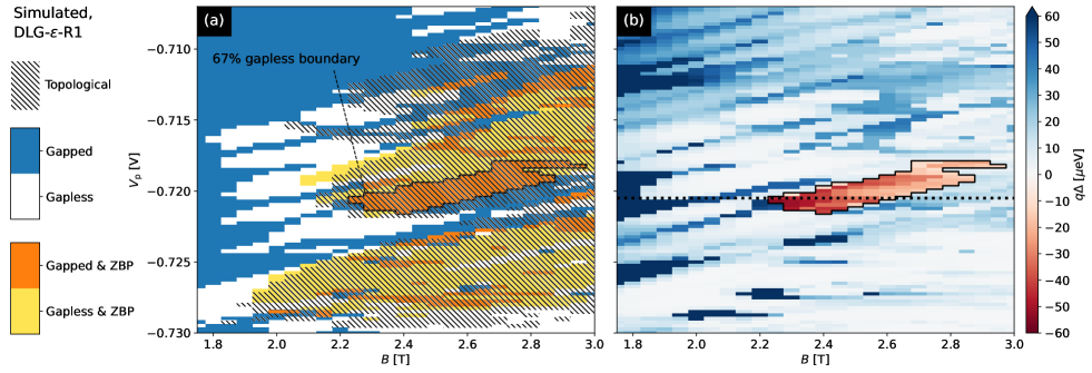
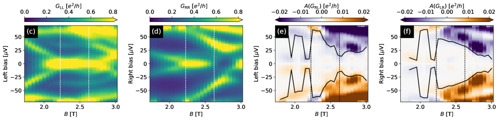
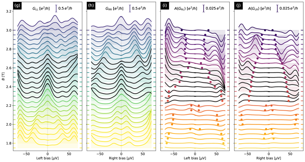
Stage 2: In Stage 2, we focus on the neighborhood of the ROI1 identified in Stage 1. Stage 2 analyzes local and non-local transport data over a range of bias voltages. In the simulated data, unlike in the experimental data discussed in Sec. 4, there is no drift of the plunger gate voltage , so the ROI1 is automatically recovered from local transport data. However, we do obtain the dependence of and on the bias voltage, as seen in Fig. 26(c,d). The more significant new ingredient in Stage 2 is the bias-dependence of the non-local conductances and , from which we determine the transport gap as a function of and . For simulated disorder realization DLG--R1, the non-local conductances , and the derived gap (indicated by black curves) as a function of for V are shown in Fig. 26(e,f). We give significant digits after the decimal point for so that these values can serve as indices in the relevant data files; this may be convenient for readers wishing to look directly at the data underlying the figures in this paper. Note that this cut passes through the topological phase transition and the topological phase; a gap closing and re-opening is seen in and . Combining the local and non-local information, we can classify any point in phase space as gapped without stable ZBPs, gapped with stable ZBPs, gapless without stable ZBPs, or gapless with stable ZBPs. These are depicted in Fig. 26(a) as, respectively, blue, orange, white, or yellow. If an orange region is surrounded by white or yellow along more than of its boundary, we identify it as an SOI2, and give it a black boundary in Fig. 26(a).
In addition to stable ZBPs, we also observe some zero-energy states that have a non-topological origin, as noted in our Stage 1 analysis. These trivial Andreev bound states (ABS) can be caused by resonances arising from the local electrostatic potential, local disorder, or a combination. We give some examples of their spectroscopy in Sec. D.5. While the presence of these ABSs can be limited by careful design of the junctions, they can never be fully suppressed. When running the TGP in experiments, we take care to tune away from pathological points in junction phase space as much as possible, while stepping between different junction configurations as we tune to span from to .
As we can see in Fig. 26(a,b), the TGP finds a region of topological phase [shown in orange in panel (a) and red in panel (b)] around T, V with a maximum topological gap , which is the upper quintile of the gaps extracted in the SOI2.
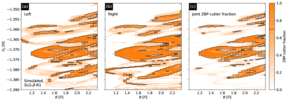
The topological gap increases from zero at the phase transition to in such a way that its median value over the red region within the black line in Fig. 26(b) is . The TGP phase diagram is compared with the scattering invariant. In Fig. 26(a), the region with is hatched. As may be seen in Fig. 26(a), the region identified by the TGP lies almost entirely within the region with negative topological index, i.e. the TGP is fairly conservative and identifies a subset of the topological phase. It is not a perfect match, of course, since the TGP is not directly calculating the scattering invariant and, moreover, the phase transition is rounded by finite temperature and finite-size corrections. Note the similarity between the hatched regions with negative topological index in Fig. 26(a) and the bright orange regions. The regions that pass the TGP are smaller pockets within these splinters.
Fig. 26(b) is another version of the phase diagram for this disorder realization: it shows the transport gap extracted from and multiplied by , depending on whether that point lies outside or inside the SOI2. Note that is not the same as the topological invariant that is used analogously in the color scale in Fig. 4 (where is the Pfaffian invariant); rather, is the proxy for that results from the TGP. The color scale of Fig. 26(b) can be viewed intuitively as the magnitude of the bulk gap multiplied by a proxy for the sign of the topological invariant. Darker red corresponds to larger topological gap.
As expected, there are some points along the boundary of the SOI2 where the closing is not visible in either or . For this cutter gate pair in this particular disorder realization, 67% of the boundary of the SOI2 shows a gap closing in , , which is above .
A comparison between the orange region in Fig. 26(a) and the hatched region lends credence to the idea that the part of the boundary that is gapped is not actually a boundary at all, and the true boundary is at higher and lower . The blue region below and to the right of the orange region is hatched, indicating that it has been misclassified as non-topological. However, as may be seen in Fig. 26(b), this gapped (and ostensibly topological) region below and to the right of the SOI2 is light blue, indicating that it has a small gap. Hence, if it were topological, it would have a small topological gap and would not be useful for a topological qubit, in contrast to the darkest red regions within the SOI2. The same observation applies to all of the hatched region that lies outside of the SOI2: it may be topological, but it has a small transport gap. Moreover, since they do not have stable ZBPs in and/or , it is unlikely that it would be possible to couple to these ZBPs in a qubit.
In this section, we discussed a disorder realization for a DLG- device that passed both Stages of the TGP and correctly found the topological phase. In Sec. D.5, we will show additional data from calibration simulations and discuss examples that fail the TGP.
D.5 Simulated disorder realizations used for the calibration of TGP
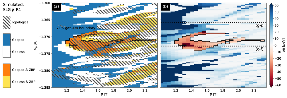
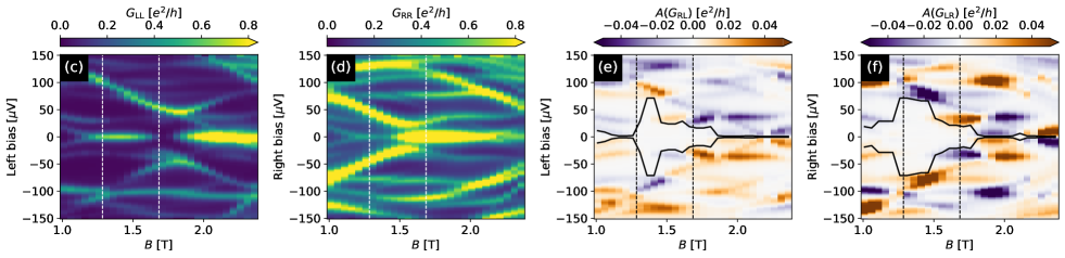
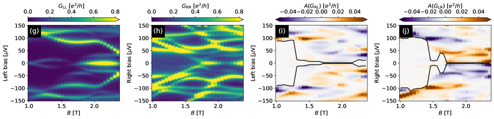
In this Appendix, we discuss two examples of simulated data that was used to calibrate the TGP. One example passes the TGP and one fails. The parameters of the simulation are equivalent to those of SLG- devices with a larger spin-orbit coupling .
The first realization, called SLG--R1, represents the -long device with . Here we assume mK. Stage 1 data is shown in Fig. 27. There are stable ZBP clusters in and as well as accidental ZBPs present for some cutter settings which correspond to disorder-induced subgap states at the junction. Due to the larger level of disorder in SLG--R1 than in DLG--R1, there are more such accidental sub-gap states than in Fig. 25. The joint ZBP map is shown in Fig. 27(c).
The Stage 2 analysis of simulated device SLG--R1 is presented in Fig. 28. Simulated device SLG--R1 has an SOI2 around . 71% of the boundary of of this SOI2 is gapless; the maximum and median topological gaps are and , respectively, for this cutter gate setting. Local and non-local conductances for V are shown in Fig. 28(c-f). There are stable ZBPs at both junctions over a range of fields of extent -T, and there is a clear gap closing and re-opening as a function of . Also, note the similarity between the hatched regions with negative SI in Fig. 28(a) and the bright orange regions in the simulated Stage 1 data in Fig. 27.
For the sake of comparison, we also present trivial ZBPs seen at a different value of V in Fig. 28(g-j) [see upper dotted line in Fig. 28(b)]. However, the non-local conductance data in Fig. 28(i,j) clearly show that the system is gapless over the corresponding range of field values.
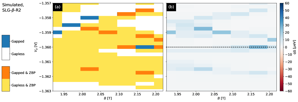
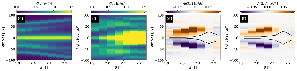
In Fig. 29, we present Stage 2 of TGP for another disorder realization, which we call SLG--R2. This is one of the realizations that passed Stage 1 but failed Stage 2. There are stable ZBPs at both junctions around V, as may be seen in Fig. 29(c,d). However, the non-local conductances in Fig. 29(e,f) yield zero gap. In fact, the, system is gapless over most of the scanned region, so this simulated transport data does not pass Stage 2 of the TGP. This example once again reinforces the fact that local measurements alone cannot reliably detect a topological phase.
Appendix E Three-terminal conductance measurements with several hundred Hz excitations
The conductance matrix is measured with a standard lock-in technique, applying simultaneous voltage excitations with amplitudes and to the inputs of the left and right terminals, respectively. They are at frequencies and , respectively, and currents and are measured at the left terminal while and are measured at the right terminal. However, due to the finite impedance network between the signal input and the measured sample, the voltages applied and the currents measured deviate from those at the sample inputs. At lock-in frequencies of several hundred Hz, the capacitances of the cryostat lines and filters (on the order of several ) combined with the line and filter resistances have a non-negligible contribution to the measured currents. Furthermore, a finite resistance at the drain contact imposes an effective voltage modulation of the opposing contact as a voltage divider effect. As a result, the sample experiences voltage modulations and at the left and and at the right input. The currents at the the left terminal are and while the currents at the right terminal are and . Noting that where , the conductances are obtained from
| (23) |
Note that we recover Eq. 2 if we take . To proceed, we need a map
| (24) |
between the voltages and currents at the sample, and , and the voltages applied and the currents measured, and :
| (25) |
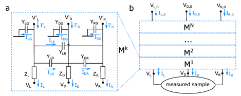
The impedance network between the input ports and the measured sample consists of a sequence of stages, each of which has the general form illustrated in Fig. 30(a): every line has a capacitance to ground and to every other line in parallel and a resistance in series to the next stage. The drain of the measured device is also connected to ground at the input and is thus included in the circuit here and will be reduced from the final mapping later. By denoting the terminals as and (where G denotes ground), the output voltages and currents are determined by the input voltages and currents , as well as cross-currents as
| (26) |
| (27) |
where are the impedances (resistances for sufficiently low frequencies) of the lines, are the parallel admittances via capacitors between and , and . Equations (26) and (27) can be expressed in matrix form as
| (28) |
This has the general form
| (29) |
With multiple stages in a sequence, the mapping from the input to the measured device
| (30) |
is given by matrix multiplication where the matrices are given by Eq. 28. The map is further reduced to a more useful form by the following steps:
-
1.
Imposing current conservation () at the sample, which then reduces the map to a matrix with and which now takes the form
(31) -
2.
Defining and as potentials with respect to at the sample, as well as , which leads to the final matrix M with and that takes the form
(32)
The effect on input voltages and measured currents of additional filtration from the measurement instruments should also be incorporated.
For our setup, the mapping M is comprised of four stages where the resistances are determined by the installed filters and, for the final stage, are the sample lead resistances which are extracted independently from the linear - response in DC measurements. To calibrate the capacitances in the setup, we measure and as a function of the excitation frequency of a voltage modulation first applied to the left port, then as a function of frequency of the modulation applied to the right port when the device is fully pinched off (i.e. the zero conductance limit). We then use capacitances between the lines and the ground as fit parameters relating the measured to and to . Finally, the mutual capacitance between and is obtained as a fit parameter relating the measured and to and , respectively. In the experiments described in the main text, the extracted capacitances of the fridge lines and filters, together with known cut-off frequencies of the voltage sources and current preamplifier outputs, are then used to calculate the sample conductances based on the measured and . Full details on this calibration routine, including all extracted parameters that were used to process measured data, can be found in the accompanying data repository [96].
Note that a further effect of finite resistances on the stages of the measurement circuit is to rescale the applied DC bias voltages. As described in [150], the DC voltages at the sample are related to the applied DC voltages and DC currents through the relationship:
| (33) |
where is a matrix containing the total resistances on the left, right and drain lines:
| (34) |
For all the experimental datasets presented in this manuscript, the average magnitude of these corrections is 1%-6% of the applied bias voltages. For this reason, we do not apply these corrections and present the data as a function of the applied bias voltages, and not of the bias voltages at the sample.
References
- Kitaev [2003] A. Y. Kitaev, Fault-tolerant quantum computation by anyons, Ann. Phys. 303, 2 (2003), quant-ph/9707021 .
- Freedman [1998] M. H. Freedman, /, and the quantum field computer, Proc. Natl. Acad. Sci. USA 95, 98 (1998).
- Nayak et al. [2008] C. Nayak, S. H. Simon, A. Stern, M. Freedman, and S. Das Sarma, Non-Abelian anyons and topological quantum computation, Rev. Mod. Phys. 80, 1083 (2008), arXiv:0707.1889 .
- Alicea [2012] J. Alicea, New directions in the pursuit of Majorana fermions in solid state systems, Rep. Prog. Phys. 75, 076501 (2012), arXiv:1202.1293 .
- Sarma et al. [2015] S. D. Sarma, M. Freedman, and C. Nayak, Majorana zero modes and topological quantum computation, npj Quantum Inf. 1, 1 (2015).
- Aasen et al. [2016] D. Aasen, M. Hell, R. V. Mishmash, A. Higginbotham, J. Danon, M. Leijnse, T. S. Jespersen, J. A. Folk, C. M. Marcus, K. Flensberg, and J. Alicea, Milestones toward Majorana-based quantum computing, Phys. Rev. X 6, 031016 (2016), arXiv:1511.05153 .
- von Burg et al. [2021] V. von Burg, G. H. Low, T. Häner, D. S. Steiger, M. Reiher, M. Roetteler, and M. Troyer, Quantum computing enhanced computational catalysis, Phys. Rev. Research 3, 033055 (2021).
- Pikulin et al. [2021] D. I. Pikulin, B. van Heck, T. Karzig, E. A. Martinez, B. Nijholt, T. Laeven, G. W. Winkler, J. D. Watson, S. Heedt, M. Temurhan, V. Svidenko, R. M. Lutchyn, M. Thomas, G. de Lange, L. Casparis, and C. Nayak, Protocol to identify a topological superconducting phase in a three-terminal device (2021), arXiv:2103.12217 .
- Kitaev [2001] A. Y. Kitaev, Unpaired Majorana fermions in quantum wires, Phys.-Usp. 44, 31 (2001), arXiv:cond-mat/0010440 .
- Sau et al. [2010a] J. D. Sau, R. M. Lutchyn, S. Tewari, and S. Das Sarma, Generic new platform for topological quantum computation using semiconductor heterostructures, Phys. Rev. Lett. 104, 040502 (2010a), arXiv:0907.2239 .
- Lutchyn et al. [2010] R. M. Lutchyn, J. D. Sau, and S. Das Sarma, Majorana Fermions and a topological phase transition in semiconductor-superconductor heterostructures, Phys. Rev. Lett. 105, 077001 (2010), arXiv:1002.4033 .
- Oreg et al. [2010] Y. Oreg, G. Refael, and F. von Oppen, Helical liquids and Majorana bound states in quantum wires, Phys. Rev. Lett. 105, 177002 (2010), arXiv:1003.1145 .
- Kitaev [2006] A. Kitaev, Anyons in an exactly solved model and beyond, Ann. Phys. 321, 2 (2006), arXiv:cond-mat/0506438 .
- Bonderson [2021] P. Bonderson, Measuring topological order, Phys. Rev. Research 3, 033110 (2021).
- de C. Chamon et al. [1997] C. de C. Chamon, D. E. Freed, S. A. Kivelson, S. L. Sondhi, and X. G. Wen, Two point-contact interferometer for quantum Hall systems, Phys. Rev. B 55, 2331 (1997).
- Fradkin et al. [1998] E. Fradkin, C. Nayak, A. Tsvelik, and F. Wilczek, A Chern-Simons effective field theory for the Pfaffian quantum Hall state, Nucl. Phys. B 516, 704 (1998), arXiv:cond-mat/9711087 .
- Bonderson et al. [2006] P. Bonderson, A. Kitaev, and K. Shtengel, Detecting non-Abelian statistics in the fractional quantum Hall state, Phys. Rev. Lett. 96, 016803 (2006), arXiv:cond-mat/0508616 .
- Stern and Halperin [2006] A. Stern and B. I. Halperin, Proposed experiments to probe the non-Abelian quantum Hall state, Phys. Rev. Lett. 96, 016802 (2006), arXiv:cond-mat/0508447 .
- Willett et al. [2010] R. L. Willett, L. N. Pfeiffer, and K. W. West, Alternation and interchange of e/4 and e/2 period interference oscillations consistent with filling factor 5/2 non-Abelian quasiparticles, Phys. Rev. B 82, 205301 (2010), arXiv:0911.0345 .
- Grenier et al. [2011] C. Grenier, R. Hervé, G. Fève, and P. Degiovanni, Electron quantum optics in quantum Hall edge channels, Mod. Phys. Lett. B 25, 1053 (2011), arXiv:1102.0466 .
- Banerjee et al. [2018] M. Banerjee, M. Heiblum, V. Umansky, D. E. Feldman, Y. Oreg, and A. Stern, Observation of half-integer thermal Hall conductance, Nature 559, 205 (2018).
- Nakamura et al. [2020] J. Nakamura, S. Liang, G. C. Gardner, and M. J. Manfra, Direct observation of anyonic braiding statistics, Nat. Phys. 16, 931 (2020).
- Law et al. [2009] K. T. Law, P. A. Lee, and T. K. Ng, Majorana fermion induced resonant Andreev reflection, Phys. Rev. Lett. 103, 237001 (2009).
- Sau et al. [2010b] J. D. Sau, S. Tewari, R. M. Lutchyn, T. D. Stanescu, and S. Das Sarma, Non-Abelian quantum order in spin-orbit-coupled semiconductors: Search for topological Majorana particles in solid-state systems, Phys. Rev. B 82, 214509 (2010b).
- Flensberg [2010] K. Flensberg, Tunneling characteristics of a chain of Majorana bound states, Phys. Rev. B 82, 180516 (2010).
- Wimmer et al. [2011] M. Wimmer, A. R. Akhmerov, J. P. Dahlhaus, and C. W. J. Beenakker, Quantum point contact as a probe of a topological superconductor, New J. Phys. 13, 053016 (2011).
- Stanescu et al. [2011] T. D. Stanescu, R. M. Lutchyn, and S. Das Sarma, Majorana fermions in semiconductor nanowires, Phys. Rev. B 84, 144522 (2011), arXiv:1106.3078 .
- Fidkowski et al. [2012] L. Fidkowski, J. Alicea, N. H. Lindner, R. M. Lutchyn, and M. P. A. Fisher, Universal transport signatures of Majorana fermions in superconductor-Luttinger liquid junctions, Phys. Rev. B 85, 245121 (2012).
- Mourik et al. [2012] V. Mourik, K. Zuo, S. M. Frolov, S. R. Plissard, E. P. A. M. Bakkers, and L. P. Kouwenhoven, Signatures of Majorana fermions in hybrid superconductor-semiconductor nanowire devices, Science 336, 1003 (2012), arXiv:1204.2792 .
- Das et al. [2012] A. Das, Y. Ronen, Y. Most, Y. Oreg, M. Heiblum, and H. Shtrikman, Zero-bias peaks and splitting in an Al-InAs nanowire topological superconductor as a signature of Majorana fermions, Nat. Phys. 8, 887 (2012), arXiv:1205.7073 .
- Deng et al. [2012] M. T. Deng, C. L. Yu, G. Y. Huang, M. Larsson, P. Caroff, and H. Q. Xu, Anomalous zero-bias conductance peak in a Nb–InSb nanowire–Nb hybrid device, Nano Lett. 12, 6414 (2012), arXiv:1204.4130 .
- Finck et al. [2013] A. D. K. Finck, D. J. Van Harlingen, P. K. Mohseni, K. Jung, and X. Li, Anomalous modulation of a zero-bias peak in a hybrid nanowire-superconductor device, Phys. Rev. Lett. 110, 126406 (2013).
- Churchill et al. [2013] H. O. H. Churchill, V. Fatemi, K. Grove-Rasmussen, M. T. Deng, P. Caroff, H. Q. Xu, and C. M. Marcus, Superconductor-nanowire devices from tunneling to the multichannel regime: Zero-bias oscillations and magnetoconductance crossover, Phys. Rev. B 87, 241401 (2013), arXiv:1303.2407 .
- Deng et al. [2016] M. T. Deng, S. Vaitiekenas, E. B. Hansen, J. Danon, M. Leijnse, K. Flensberg, J. Nygård, P. Krogstrup, and C. M. Marcus, Majorana bound state in a coupled quantum-dot hybrid-nanowire system, Science 354, 1557 (2016).
- Nichele et al. [2017] F. Nichele, A. C. C. Drachmann, A. M. Whiticar, E. C. T. O’Farrell, H. J. Suominen, A. Fornieri, T. Wang, G. C. Gardner, C. Thomas, A. T. Hatke, P. Krogstrup, M. J. Manfra, K. Flensberg, and C. M. Marcus, Scaling of Majorana zero-bias conductance peaks, Phys. Rev. Lett. 119, 136803 (2017).
- Vaitiekėnas et al. [2018] S. Vaitiekėnas, M.-T. Deng, J. Nygård, P. Krogstrup, and C. M. Marcus, Effective factor of subgap states in hybrid nanowires, Phys. Rev. Lett. 121, 037703 (2018).
- de Moor et al. [2018] M. W. A. de Moor, J. D. S. Bommer, D. Xu, G. W. Winkler, A. E. Antipov, A. Bargerbos, G. Wang, N. van Loo, R. L. M. O. het Veld, S. Gazibegovic, D. Car, J. A. Logan, M. Pendharkar, J. S. Lee, E. P. A. M. Bakkers, C. J. Palmstrøm, R. M. Lutchyn, L. P. Kouwenhoven, and H. Zhang, Electric field tunable superconductor-semiconductor coupling in Majorana nanowires, New J. Phys. 20, 103049 (2018).
- Lutchyn et al. [2018] R. M. Lutchyn, E. P. A. M. Bakkers, L. P. Kouwenhoven, P. Krogstrup, C. M. Marcus, and Y. Oreg, Majorana zero modes in superconductor-semiconductor heterostructures, Nat. Rev. Mater. 3, 52 (2018).
- Anselmetti et al. [2019] G. L. R. Anselmetti, E. A. Martinez, G. C. Ménard, D. Puglia, F. K. Malinowski, J. S. Lee, S. Choi, M. Pendharkar, C. J. Palmstrøm, C. M. Marcus, L. Casparis, and A. P. Higginbotham, End-to-end correlated subgap states in hybrid nanowires, Phys. Rev. B 100, 205412 (2019).
- Zhang et al. [2021] H. Zhang, M. W. A. de Moor, J. D. S. Bommer, D. Xu, G. Wang, N. van Loo, C.-X. Liu, S. Gazibegovic, J. A. Logan, D. Car, R. L. M. O. h. Veld, P. J. van Veldhoven, S. Koelling, M. A. Verheijen, M. Pendharkar, D. J. Pennachio, B. Shojaei, J. S. Lee, C. J. Palmstrøm, E. P. A. M. Bakkers, S. D. Sarma, and L. P. Kouwenhoven, Large zero-bias peaks in InSb-Al hybrid semiconductor-superconductor nanowire devices (2021), arXiv:2101.11456 .
- Vaitiekenas et al. [2020] S. Vaitiekenas, G. W. Winkler, B. van Heck, T. Karzig, M.-T. Deng, K. Flensberg, L. I. Glazman, C. Nayak, P. Krogstrup, R. M. Lutchyn, and C. M. Marcus, Flux-induced topological superconductivity in full-shell nanowires, Science 367, eaav3392 (2020).
- Banerjee et al. [2022a] A. Banerjee, O. Lesser, M. A. Rahman, H. R. Wang, M. R. Li, A. Kringhøj, A. M. Whiticar, A. C. C. Drachmann, C. Thomas, T. Wang, M. J. Manfra, E. Berg, Y. Oreg, A. Stern, and C. M. Marcus, Signatures of a topological phase transition in a planar Josephson junction (2022a), arXiv:2201.03453 .
- Bagrets and Altland [2012] D. Bagrets and A. Altland, Class spectral peak in Majorana quantum wires, Phys. Rev. Lett. 109, 227005 (2012), arXiv:1206.0434 .
- Pikulin et al. [2012] D. I. Pikulin, J. P. Dahlhaus, M. Wimmer, H. Schomerus, and C. W. J. Beenakker, A zero-voltage conductance peak from weak antilocalization in a Majorana nanowire, New J. Phys. 14, 125011 (2012).
- Pan and Das Sarma [2022] H. Pan and S. Das Sarma, On-demand large conductance in trivial zero-bias tunneling peaks in Majorana nanowires, Phys. Rev. B 105, 115432 (2022).
- Prada et al. [2012] E. Prada, P. San-Jose, and R. Aguado, Transport spectroscopy of nanowire junctions with Majorana fermions, Phys. Rev. B 86, 180503 (2012), arXiv:1203.4488 .
- Kells et al. [2012] G. Kells, D. Meidan, and P. W. Brouwer, Near-zero-energy end states in topologically trivial spin-orbit coupled superconducting nanowires with a smooth confinement, Phys. Rev. B 86, 100503 (2012).
- Stanescu and Tewari [2014] T. D. Stanescu and S. Tewari, Nonlocality of zero-bias anomalies in the topologically trivial phase of Majorana wires, Phys. Rev. B 89, 220507 (2014).
- Liu et al. [2017] C.-X. Liu, J. D. Sau, T. D. Stanescu, and S. Das Sarma, Andreev bound states versus Majorana bound states in quantum dot-nanowire-superconductor hybrid structures: Trivial versus topological zero-bias conductance peaks, Phys. Rev. B 96, 075161 (2017).
- Vuik et al. [2019] A. Vuik, B. Nijholt, A. R. Akhmerov, and M. Wimmer, Reproducing topological properties with quasi-Majorana states, SciPost Phys. 7, 061 (2019).
- Pan et al. [2021a] H. Pan, C.-X. Liu, M. Wimmer, and S. Das Sarma, Quantized and unquantized zero-bias tunneling conductance peaks in Majorana nanowires: Conductance below and above , Phys. Rev. B 103, 214502 (2021a).
- Lee et al. [2012] E. J. H. Lee, X. Jiang, R. Aguado, G. Katsaros, C. M. Lieber, and S. De Franceschi, Zero-bias anomaly in a nanowire quantum dot coupled to superconductors, Phys. Rev. Lett. 109, 186802 (2012), arXiv:1207.1259 .
- Reeg et al. [2018a] C. Reeg, O. Dmytruk, D. Chevallier, D. Loss, and J. Klinovaja, Zero-energy Andreev bound states from quantum dots in proximitized Rashba nanowires, Phys. Rev. B 98, 245407 (2018a).
- Yu et al. [2020] W. Yu, R. Haenel, M. A. Rodriguez, S. R. Lee, F. Zhang, M. Franz, D. I. Pikulin, and W. Pan, Zero-bias conductance peak in dirac semimetal-superconductor devices, Phys. Rev. Research 2, 032002 (2020).
- Lee et al. [2013] E. J. H. Lee, X. Jiang, M. Houzet, R. Aguado, C. M. Lieber, and S. D. Franceschi, Spin-resolved Andreev levels and parity crossings in hybrid superconductor–semiconductor nanostructures, Nat. Nanotechnol. 9, 79 (2013).
- Suominen et al. [2017] H. J. Suominen, M. Kjaergaard, A. R. Hamilton, J. Shabani, C. J. Palmstrøm, C. M. Marcus, and F. Nichele, Zero-energy modes from coalescing Andreev states in a two-dimensional semiconductor-superconductor hybrid platform, Phys. Rev. Lett. 119, 176805 (2017).
- Pan et al. [2020] H. Pan, W. S. Cole, J. D. Sau, and S. Das Sarma, Generic quantized zero-bias conductance peaks in superconductor-semiconductor hybrid structures, Phys. Rev. B 101, 024506 (2020).
- Read and Green [2000] N. Read and D. Green, Paired states of fermions in two dimensions with breaking of parity and time-reversal symmetries and the fractional quantum Hall effect, Phys. Rev. B 61, 10267 (2000).
- Antipov et al. [2018] A. E. Antipov, A. Bargerbos, G. W. Winkler, B. Bauer, E. Rossi, and R. M. Lutchyn, Effects of gate-induced electric fields on semiconductor Majorana nanowires, Phys. Rev. X 8, 031041 (2018).
- Winkler et al. [2019] G. W. Winkler, A. E. Antipov, B. van Heck, A. A. Soluyanov, L. I. Glazman, M. Wimmer, and R. M. Lutchyn, Unified numerical approach to topological semiconductor-superconductor heterostructures, Phys. Rev. B 99, 245408 (2019).
- Nadj-Perge et al. [2013] S. Nadj-Perge, I. K. Drozdov, B. A. Bernevig, and A. Yazdani, Proposal for realizing majorana fermions in chains of magnetic atoms on a superconductor, Phys. Rev. B 88, 020407 (2013).
- Klinovaja et al. [2013] J. Klinovaja, P. Stano, A. Yazdani, and D. Loss, Topological superconductivity and majorana fermions in RKKY systems, Physical Review Letters 111, 10.1103/physrevlett.111.186805 (2013).
- Braunecker and Simon [2013] B. Braunecker and P. Simon, Interplay between classical magnetic moments and superconductivity in quantum one-dimensional conductors: Toward a self-sustained topological majorana phase, Physical Review Letters 111, 10.1103/physrevlett.111.147202 (2013).
- Pientka et al. [2013] F. Pientka, L. I. Glazman, and F. von Oppen, Topological superconducting phase in helical shiba chains, Phys. Rev. B 88, 155420 (2013).
- Nadj-Perge et al. [2014] S. Nadj-Perge, I. K. Drozdov, J. Li, H. Chen, S. Jeon, J. Seo, A. H. MacDonald, B. A. Bernevig, and A. Yazdani, Observation of Majorana fermions in ferromagnetic atomic chains on a superconductor, Science 346, 602 (2014), arXiv:1410.0682 .
- Cook and Franz [2011] A. Cook and M. Franz, Majorana fermions in a topological-insulator nanowire proximity-coupled to an -wave superconductor, Phys. Rev. B 84, 201105 (2011).
- Hosur et al. [2011] P. Hosur, P. Ghaemi, R. S. K. Mong, and A. Vishwanath, Majorana modes at the ends of superconductor vortices in doped topological insulators, Phys. Rev. Lett. 107, 097001 (2011).
- Fu and Kane [2008] L. Fu and C. L. Kane, Superconducting proximity effect and Majorana fermions at the surface of a topological insulator, Phys. Rev. Lett. 100, 096407 (2008), arXiv:0707.1692 .
- Fu and Kane [2009] L. Fu and C. L. Kane, Josephson current and noise at a superconductor/quantum-spin-Hall-insulator/superconductor junction, Phys. Rev. B 79, 161408(R) (2009).
- Hasan and Kane [2010] M. Z. Hasan and C. L. Kane, Colloquium: Topological insulators, Rev. Mod. Phys. 82, 3045 (2010).
- Alicea [2010] J. Alicea, Majorana fermions in a tunable semiconductor device, Phys. Rev. B 81, 125318 (2010).
- Sau et al. [2010] J. D. Sau, S. Tewari, R. M. Lutchyn, T. D. Stanescu, and S. Das Sarma, Non-Abelian quantum order in spin-orbit-coupled semiconductors: Search for topological Majorana particles in solid-state systems, Phys. Rev. B 82, 214509 (2010), arXiv:1006.2829 .
- Chung et al. [2011] S. B. Chung, H.-J. Zhang, X.-L. Qi, and S.-C. Zhang, Topological superconducting phase and Majorana fermions in half-metal/superconductor heterostructures, Phys. Rev. B 84, 060510 (2011).
- Duckheim and Brouwer [2011] M. Duckheim and P. W. Brouwer, Andreev reflection from noncentrosymmetric superconductors and Majorana bound-state generation in half-metallic ferromagnets, Phys. Rev. B 83, 054513 (2011).
- Potter and Lee [2012] A. C. Potter and P. A. Lee, Topological superconductivity and Majorana fermions in metallic surface states, Phys. Rev. B 85, 094516 (2012).
- Sato et al. [2009] M. Sato, Y. Takahashi, and S. Fujimoto, Non-Abelian topological order in -wave superfluids of ultracold fermionic atoms, Phys. Rev. Lett. 103, 020401 (2009), arXiv:0901.4693 .
- Zhang et al. [2008] C. Zhang, S. Tewari, R. M. Lutchyn, and S. Das Sarma, superfluid from -wave interactions of fermionic cold atoms, Phys. Rev. Lett. 101, 160401 (2008).
- Vuik et al. [2016] A. Vuik, D. Eeltink, A. R. Akhmerov, and M. Wimmer, Effects of the electrostatic environment on the Majorana nanowire devices, New J. Phys. 18, 033013 (2016), arXiv:1511.08044 .
- Mikkelsen et al. [2018] A. E. G. Mikkelsen, P. Kotetes, P. Krogstrup, and K. Flensberg, Hybridization at superconductor-semiconductor interfaces, Phys. Rev. X 8, 031040 (2018).
- Winkler et al. [2017] G. W. Winkler, D. Varjas, R. Skolasinski, A. A. Soluyanov, M. Troyer, and M. Wimmer, Orbital contributions to the electron factor in semiconductor nanowires, Phys. Rev. Lett. 119, 037701 (2017).
- Nijholt and Akhmerov [2016] B. Nijholt and A. R. Akhmerov, Orbital effect of magnetic field on the Majorana phase diagram, Phys. Rev. B 93, 235434 (2016), arXiv:1509.02675 .
- Schuwalow et al. [2021] S. Schuwalow, N. B. M. Schröter, J. Gukelberger, C. Thomas, V. Strocov, J. Gamble, A. Chikina, M. Caputo, J. Krieger, G. C. Gardner, M. Troyer, G. Aeppli, M. J. Manfra, and P. Krogstrup, Band structure extraction at hybrid narrow-gap semiconductor–metal interfaces, Adv. Sci. 8, 2003087 (2021).
- Chauhan et al. [2022] P. Chauhan, C. Thomas, T. Lindemann, G. C. Gardner, J. Gukelberger, M. J. Manfra, and N. P. Armitage, Measurements of cyclotron resonance of the interfacial states in strong spin–orbit coupled 2D electron gases proximitized with aluminum, Appl. Phys. Lett. 120, 142105 (2022).
- Hart et al. [2019] S. Hart, Z. Cui, G. Ménard, M. Deng, A. E. Antipov, R. M. Lutchyn, P. Krogstrup, C. M. Marcus, and K. A. Moler, Current-phase relations of InAs nanowire Josephson junctions: From interacting to multimode regimes, Phys. Rev. B 100, 064523 (2019).
- Kringhøj et al. [2021] A. Kringhøj, G. W. Winkler, T. W. Larsen, D. Sabonis, O. Erlandsson, P. Krogstrup, B. van Heck, K. D. Petersson, and C. M. Marcus, Andreev modes from phase winding in a full-shell nanowire-based transmon, Phys. Rev. Lett. 126, 047701 (2021).
- Shen et al. [2021] J. Shen, G. W. Winkler, F. Borsoi, S. Heedt, V. Levajac, J.-Y. Wang, D. van Driel, D. Bouman, S. Gazibegovic, R. L. M. Op Het Veld, D. Car, J. A. Logan, M. Pendharkar, C. J. Palmstrøm, E. P. A. M. Bakkers, L. P. Kouwenhoven, and B. van Heck, Full parity phase diagram of a proximitized nanowire island, Phys. Rev. B 104, 045422 (2021).
- Rosdahl et al. [2018] T. Ö. Rosdahl, A. Vuik, M. Kjaergaard, and A. R. Akhmerov, Andreev rectifier: A nonlocal conductance signature of topological phase transitions, Phys. Rev. B 97, 045421 (2018), arXiv:1706.08888 .
- Ménard et al. [2020] G. C. Ménard, G. L. R. Anselmetti, E. A. Martinez, D. Puglia, F. K. Malinowski, J. S. Lee, S. Choi, M. Pendharkar, C. J. Palmstrøm, K. Flensberg, C. M. Marcus, L. Casparis, and A. P. Higginbotham, Conductance-matrix symmetries of a three-terminal hybrid device, Phys. Rev. Lett. 124, 036802 (2020).
- Puglia et al. [2021] D. Puglia, E. A. Martinez, G. C. Mé nard, A. Pöschl, S. Gronin, G. C. Gardner, R. Kallaher, M. J. Manfra, C. M. Marcus, A. P. Higginbotham, and L. Casparis, Closing of the induced gap in a hybrid superconductor-semiconductor nanowire, Phys. Rev. B 103, 235201 (2021).
- Pöschl et al. [2022] A. Pöschl, A. Danilenko, D. Sabonis, K. Kristjuhan, T. Lindemann, C. Thomas, M. J. Manfra, and C. M. Marcus, Nonlocal conductance spectroscopy of Andreev bound states in gate-defined InAs/Al nanowires (2022), arXiv:2204.02430 .
- Banerjee et al. [2022b] A. Banerjee, O. Lesser, M. A. Rahman, C. Thomas, T. Wang, M. J. Manfra, E. Berg, Y. Oreg, A. Stern, and C. M. Marcus, Local and nonlocal transport spectroscopy in planar Josephson junctions (2022b), arXiv:2205.09419 .
- Hess et al. [2021] R. Hess, H. F. Legg, D. Loss, and J. Klinovaja, Local and nonlocal quantum transport due to Andreev bound states in finite Rashba nanowires with superconducting and normal sections, Phys. Rev. B 104, 075405 (2021).
- Sticlet et al. [2017] D. Sticlet, B. Nijholt, and A. Akhmerov, Robustness of majorana bound states in the short-junction limit, Phys. Rev. B 95, 115421 (2017).
- Reeg et al. [2018b] C. Reeg, D. Loss, and J. Klinovaja, Metallization of a Rashba wire by a superconducting layer in the strong-proximity regime, Phys. Rev. B 97, 165425 (2018b).
- Cole et al. [2015] W. S. Cole, S. Das Sarma, and T. D. Stanescu, Effects of large induced superconducting gap on semiconductor Majorana nanowires, Phys. Rev. B 92, 174511 (2015).
- [96] The full experimental and simulated data sets and source code that performs the analysis and produces figures is available at github.com/microsoft/azure-quantum-tgp. Alternatively, for a zero-setup, in-browser notebook experience on Microsoft Azure, visit aka.ms/AQ/tgp.
- Wimmer [2012] M. Wimmer, Algorithm 923: Efficient numerical computation of the Pfaffian for dense and banded skew-symmetric matrices, ACM Trans. Math. Softw. 38, 4, Article 30 (2012).
- Lutchyn et al. [2011] R. M. Lutchyn, T. D. Stanescu, and S. Das Sarma, Search for Majorana fermions in multiband semiconducting nanowires, Phys. Rev. Lett. 106, 127001 (2011).
- Woods et al. [2021] B. D. Woods, S. Das Sarma, and T. D. Stanescu, Charge-impurity effects in hybrid Majorana nanowires, Phys. Rev. Appl. 16, 054053 (2021).
- Giamarchi [2004] T. Giamarchi, Quantum Physics in One Dimension (Oxford University Press, Oxford, 2004).
- Boutin et al. [2022] S. Boutin, A. Antipov, W. Cole, J. Gukelberger, F. Karimi, G. Winkler, B. Bauer, and R. Lutchyn, Correlated disorder in one-dimensional topological superconductors (2022), to appear.
- Wang et al. [2021] G. Wang, T. Dvir, N. van Loo, G. P. Mazur, S. Gazibegovic, G. Badawy, E. P. A. M. Bakkers, L. P. Kouwenhoven, and G. de Lange, Non-local measurement of quasiparticle distribution in proximitized semiconductor nanowires using quantum dots, arXiv:2110.05373 (2021).
- Fulga et al. [2011] I. C. Fulga, F. Hassler, A. R. Akhmerov, and C. W. J. Beenakker, Scattering formula for the topological quantum number of a disordered multimode wire, Phys. Rev. B 83, 155429 (2011).
- Akhmerov [2022] A. Akhmerov, What can we learn from the reported discovery of majorana states? (2022).
- Feshchenko et al. [2015] A. V. Feshchenko, L. Casparis, I. M. Khaymovich, D. Maradan, O.-P. Saira, M. Palma, M. Meschke, J. P. Pekola, and D. M. Zumbühl, Tunnel-junction thermometry down to millikelvin temperatures, Phys. Rev. Appl. 4, 034001 (2015).
- Willett et al. [1987] R. Willett, J. P. Eisenstein, H. L. Störmer, D. C. Tsui, A. C. Gossard, and J. H. English, Observation of an even-denominator quantum number in the fractional quantum Hall effect, Phys. Rev. Lett. 59, 1776 (1987).
- Pan et al. [1999] W. Pan, J.-S. Xia, V. Shvarts, D. E. Adams, H. L. Stormer, D. C. Tsui, L. N. Pfieffer, K. W. Baldwin, and K. W. West, Exact quantization of the even-denominator fractional quantum Hall state at Landau level filling factor, Phys. Rev. Lett. 83, 3530 (1999), arXiv:cond-mat/9907356 .
- Kumar et al. [2010] A. Kumar, G. A. Csáthy, M. J. Manfra, L. N. Pfeiffer, and K. W. West, Nonconventional odd-denominator fractional quantum Hall states in the second Landau level, Phys. Rev. Lett. 105, 246808 (2010).
- Zibrov et al. [2017] A. A. Zibrov, C. Kometter, H. Zhou, E. M. Spanton, T. Taniguchi, K. Watanabe, M. P. Zaletel, and A. F. Young, Tunable interacting composite fermion phases in a half-filled bilayer-graphene Landau level, Nature 549, 360 (2017).
- Fidkowski et al. [2011] L. Fidkowski, R. M. Lutchyn, C. Nayak, and M. P. A. Fisher, Majorana zero modes in one-dimensional quantum wires without long-ranged superconducting order, Phys. Rev. B 84, 195436 (2011), arXiv:1106.2598 .
- Karzig et al. [2017] T. Karzig, C. Knapp, R. M. Lutchyn, P. Bonderson, M. B. Hastings, C. Nayak, J. Alicea, K. Flensberg, S. Plugge, Y. Oreg, C. M. Marcus, and M. H. Freedman, Scalable designs for quasiparticle-poisoning-protected topological quantum computation with Majorana zero modes, Phys. Rev. B 95, 235305 (2017).
- Plugge et al. [2016] S. Plugge, L. A. Landau, E. Sela, A. Altland, K. Flensberg, and R. Egger, Roadmap to Majorana surface codes, Phys. Rev. B 94, 174514 (2016).
- Plugge et al. [2017] S. Plugge, A. Rasmussen, R. Egger, and K. Flensberg, Majorana box qubits, New J. Phys. 19, 012001 (2017).
- Vijay et al. [2015] S. Vijay, T. H. Hsieh, and L. Fu, Majorana fermion surface code for universal quantum computation, Phys. Rev. X 5, 041038 (2015), arXiv:1504.01724 .
- Vijay and Fu [2016] S. Vijay and L. Fu, Physical implementation of a Majorana fermion surface code for fault-tolerant quantum computation, Phys. Scr. 168, 014002 (2016), arXiv:1509.08134 .
- Vijay and Fu [2016] S. Vijay and L. Fu, Teleportation-based quantum information processing with Majorana zero modes, Phys. Rev. B 94, 235446 (2016), arXiv:1609.00950 .
- Bonderson et al. [2008] P. Bonderson, M. Freedman, and C. Nayak, Measurement-only topological quantum computation, Phys. Rev. Lett. 101, 010501 (2008), arXiv:0802.0279 .
- Bonderson et al. [2009] P. Bonderson, M. Freedman, and C. Nayak, Measurement-only topological quantum computation via anyonic interferometry, Ann. Phys. 324, 787 (2009), arXiv:0808.1933 .
- Maki [1964] K. Maki, The behavior of superconducting thin films in the presence of magnetic fields and currents, Prog. Theor. Phys. 31, 731 (1964).
- Lutchyn et al. [2012] R. M. Lutchyn, T. D. Stanescu, and S. Das Sarma, Momentum relaxation in a semiconductor proximity-coupled to a disordered -wave superconductor: Effect of scattering on topological superconductivity, Phys. Rev. B 85, 140513 (2012).
- Reeg et al. [2018c] C. Reeg, D. Loss, and J. Klinovaja, Proximity effect in a two-dimensional electron gas coupled to a thin superconducting layer, Beilstein J. Nanotechnol. 9, 1263 (2018c).
- Kiendl et al. [2019] T. Kiendl, F. von Oppen, and P. W. Brouwer, Proximity-induced gap in nanowires with a thin superconducting shell, Phys. Rev. B 100, 035426 (2019).
- Stanescu and Das Sarma [2022] T. D. Stanescu and S. Das Sarma, Proximity-induced superconductivity generated by thin films: Effects of Fermi surface mismatch and disorder in the superconductor, Phys. Rev. B 106, 085429 (2022).
- Thomas et al. [2022] S. N. Thomas, S. D. Sarma, and J. D. Sau, Disorder suppression in topological semiconductor-superconductor junctions (2022), arXiv:2207.05109 .
- Aikebaier et al. [2019] F. Aikebaier, P. Virtanen, and T. Heikkilä, Superconductivity near a magnetic domain wall, Phys. Rev. B 99, 104504 (2019).
- Khindanov et al. [2021] A. Khindanov, J. Alicea, P. Lee, W. S. Cole, and A. E. Antipov, Topological superconductivity in nanowires proximate to a diffusive superconductor–magnetic-insulator bilayer, Phys. Rev. B 103, 134506 (2021).
- Motrunich et al. [2001] O. Motrunich, K. Damle, and D. A. Huse, Griffiths effects and quantum critical points in dirty superconductors without spin-rotation invariance: One-dimensional examples, Phys. Rev. B 63, 224204 (2001).
- Gruzberg et al. [2005] I. A. Gruzberg, N. Read, and S. Vishveshwara, Localization in disordered superconducting wires with broken spin-rotation symmetry, Phys. Rev. B 71, 245124 (2005).
- Brouwer et al. [2011a] P. W. Brouwer, M. Duckheim, A. Romito, and F. von Oppen, Topological superconducting phases in disordered quantum wires with strong spin-orbit coupling, Phys. Rev. B 84, 144526 (2011a).
- Brouwer et al. [2011b] P. W. Brouwer, M. Duckheim, A. Romito, and F. von Oppen, Probability distribution of Majorana end-state energies in disordered wires, Phys. Rev. Lett. 107, 196804 (2011b).
- Lobos et al. [2012] A. M. Lobos, R. M. Lutchyn, and S. Das Sarma, Interplay of disorder and interaction in Majorana quantum wires, Phys. Rev. Lett. 109, 146403 (2012).
- Sau et al. [2012] J. D. Sau, S. Tewari, and S. Das Sarma, Experimental and materials considerations for the topological superconducting state in electron- and hole-doped semiconductors: Searching for non-Abelian Majorana modes in 1D nanowires and 2D heterostructures, Phys. Rev. B 85, 064512 (2012).
- DeGottardi et al. [2013] W. DeGottardi, D. Sen, and S. Vishveshwara, Majorana fermions in superconducting 1D systems having periodic, quasiperiodic, and disordered potentials, Phys. Rev. Lett. 110, 146404 (2013).
- De Gottardi [2012] W. De Gottardi, Strong correlations and topological order in one-dimensional systems, Ph.D. thesis, University of Illinois at Urbana-Champaign (2012).
- Adagideli et al. [2014] I. Adagideli, M. Wimmer, and A. Teker, Effects of electron scattering on the topological properties of nanowires: Majorana fermions from disorder and superlattices, Phys. Rev. B 89, 144506 (2014).
- Pekerten et al. [2017] B. Pekerten, A. Teker, O. Bozat, M. Wimmer, and I. Adagideli, Disorder-induced topological transitions in multichannel Majorana wires, Phys. Rev. B 95, 064507 (2017).
- Ahn et al. [2021] S. Ahn, H. Pan, B. Woods, T. D. Stanescu, and S. Das Sarma, Estimating disorder and its adverse effects in semiconductor Majorana nanowires, Phys. Rev. Mater. 5, 124602 (2021).
- Thouless [1973] D. Thouless, Localization distance and mean free path in one-dimensional disordered systems, J Phys. C: Solid State Phys. 6, L49 (1973).
- Vishveshwara and Fisher [2001] S. Vishveshwara and M. P. A. Fisher, Quasiparticle localization transition in dirty superconductors, Phys. Rev. B 64, 174511 (2001).
- Laroche et al. [2010] D. Laroche, S. Das Sarma, G. Gervais, M. P. Lilly, and J. L. Reno, Scattering mechanism in modulation-doped shallow two-dimensional electron gases, Appl. Phys. Lett. 96, 162112 (2010).
- Das Sarma and Hwang [2014] S. Das Sarma and E. H. Hwang, Mobility versus quality in two-dimensional semiconductor structures, Phys. Rev. B 90, 035425 (2014).
- Shojaei et al. [2016] B. Shojaei, A. C. C. Drachmann, M. Pendharkar, D. J. Pennachio, M. P. Echlin, P. G. Callahan, S. Kraemer, T. M. Pollock, C. M. Marcus, and C. J. Palmstrøm, Limits to mobility in InAs quantum wells with nearly lattice-matched barriers, Phys. Rev. B 94, 245306 (2016).
- Tschirky et al. [2017] T. Tschirky, S. Mueller, C. A. Lehner, S. Fält, T. Ihn, K. Ensslin, and W. Wegscheider, Scattering mechanisms of highest-mobility InAs/AlxGa1-xSb quantum wells, Phys. Rev. B 95, 115304 (2017).
- Hatke et al. [2017] A. T. Hatke, T. Wang, C. Thomas, G. C. Gardner, and M. J. Manfra, Mobility in excess of 106 cm2/Vs in InAs quantum wells grown on lattice mismatched InP substrates, Appl. Phys. Lett. 111, 142106 (2017).
- Thomas et al. [2018] C. Thomas, A. T. Hatke, A. Tuaz, R. Kallaher, T. Wu, T. Wang, R. E. Diaz, G. C. Gardner, M. A. Capano, and M. J. Manfra, High-mobility InAs 2DEGs on GaSb substrates: A platform for mesoscopic quantum transport, Phys. Rev. Mater. 2, 104602 (2018).
- Wickramasinghe et al. [2018] K. S. Wickramasinghe, W. Mayer, J. Yuan, T. Nguyen, L. Jiao, V. Manucharyan, and J. Shabani, Transport properties of near surface inas two-dimensional heterostructures, Appl. Phys. Lett. 113, 262104 (2018).
- Pauka et al. [2020] S. J. Pauka, J. D. S. Witt, C. N. Allen, B. Harlech-Jones, A. Jouan, G. C. Gardner, S. Gronin, T. Wang, C. Thomas, M. J. Manfra, J. Gukelberger, J. Gamble, D. J. Reilly, and M. C. Cassidy, Repairing the surface of InAs-based topological heterostructures, J. Appl. Phys. 128, 114301 (2020).
- Cimpoiasu et al. [2020] E. Cimpoiasu, M. J. Fox, B. R. Dunphy, S. Mack, J. A. Christodoulides, and B. R. Bennett, Charge scattering mechanisms in shallow InAs quantum wells, J. Appl. Phys. 127, 145702 (2020).
- Fornieri et al. [2019] A. Fornieri, A. M. Whiticar, F. Setiawan, E. Portolés, A. C. C. Drachmann, A. Keselman, S. Gronin, C. Thomas, T. Wang, R. Kallaher, G. C. Gardner, E. Berg, M. J. Manfra, A. Stern, C. M. Marcus, and F. Nichele, Evidence of topological superconductivity in planar Josephson junctions, Nature 569, 89 (2019).
- Martinez et al. [2021] E. A. Martinez, A. Pöschl, E. B. Hansen, M. A. Y. van de Poll, S. Vaitiekėnas, A. P. Higginbotham, and L. Casparis, Measurement circuit effects in three-terminal electrical transport measurements (2021), arXiv:2104.02671 .
- Maiani et al. [2022] A. Maiani, M. Geier, and K. Flensberg, Conductance-matrix symmetries of multiterminal semiconductor-superconductor devices (2022), arXiv:2205.11193 .
- Pan et al. [2021b] H. Pan, J. D. Sau, and S. Das Sarma, Three-terminal nonlocal conductance in Majorana nanowires: Distinguishing topological and trivial in realistic systems with disorder and inhomogeneous potential, Phys. Rev. B 103, 014513 (2021b).