Spin-orbit coupling and electron scattering in high-quality InSb1-xAsx quantum wells
Abstract
InSb1-xAsx is a promising material system for exploration of topological superconductivity in hybrid superconductor/semiconductor devices due to large effective -factor and enhanced spin-orbit coupling when compared to binary InSb and InAs. Much remains to be understood concerning the fundamental properties of the two-dimensional electron gas (2DEG) in InSbAs quantum wells. We report on the electrical properties of a series of 30 nm InSb1-xAsx quantum wells grown 40 nm below the surface with three different arsenic mole fractions, 0.05, 0.13, and 0.19. The dependencies of mobility on 2DEG density and arsenic mole fraction are analyzed. For the sample, the 2DEG displays a peak mobility cm2/Vs at a density of cm-2. High mobility, small effective mass, and strong spin-orbit coupling result in beating in the Shubnikov de Haas oscillations at low magnetic field. Fourier analysis of the Shubnikov de Haas oscillations facilitates extraction of the Rashba spin-orbit parameter as a function of 2DEG density and quantum well mole fraction. For at cm -2, meV Å, among the highest reported values in III-V materials.
I Introduction
Small band gap zinc-blende III-V semiconductors (such as InAs and InSb) are the subject of renewed interest as they may be utilized as a platform to explore topological superconductivity. Strong spin-orbit coupling (SOC) and proximity-induced superconductivity from a parent s-wave superconductor are key ingredients needed to realize a topological phase [1, 2, 3, 4, 5, 6, 7, 8, 9, 10, 11]. Gate-controlled SOC is of fundamental and practical interest. The ability to externally manipulate the strength of SOC in a 2DEG facilitates realization of spin dependent devices, such as the spin field effect transistor [12].
The ternary compound InSb1-xAsx is appealing compared to InSb and InAs because it is predicted to have a higher Rashba SOC parameter [13, 14, 15, 8]. The increase in SOC with arsenic mole fraction in InSb1-xAsx has been measured in nanowires [16] and recently in a surface 2DEG [11]. Here, we focus on 30 nm quantum wells buried under a 40 nm In0.88Al0.12Sb top barrier. Arsenic mole fractions of = 0.05, = 0.13, = 0.19 are used in the quantum well. Our buried quantum well design, compared to a surface layer, allows for more straightforward comparisons of the Rashba parameter between samples at nearly equal electric field and 2DEG density, as well as identification of electron scattering mechanisms over a broader range of 2DEG density. Spin-orbit coupling and the resultant zero-field spin-split bands arises from broken inversion symmetry. Inversion asymmetry may be microscopic bulk inversion asymmetry (BIA) or structural inversion asymmetry (SIA). Dresselhaus SOC is associated with the lack of inversion symmetry in the crystal lattice, e.g. zinc-blende semiconductors [17]. The Rashba mechanism is due to asymmetry in the macroscopic potential induced by an external gate and/or an asymmetric heterostructure design [18]. In heterostructures built with small bandgap III-V zinc-blende semiconductors, the Rashba coupling is usually the dominant k-linear SOC term. Values for the Rashba parameter for InSb and InAs quantum wells have been reported. Hatke et al. [19] reported 120 meVÅ in deep InAs quantum wells at 3 1011 cm-2; in modulation-doped InSb quantum wells Gilbertson et al. [20] extracted between 130-160 meVÅ for a density range of 3.15-3.30 1011 cm-2. We report Rashba coupling of 300 meVÅ in a InSb0.81As0.19 quantum well, among the highest measured in III-V semiconductors [21, 22, 23, 20, 24, 25, 26, 27, 19, 28].
| width=textwidth | As mole fraction () | at Vg = 0 V ( cm-2) | at cm-2 (cm2/Vs) | m* (me) |
|---|---|---|---|---|
| Sample A | 0.05 | 0.6 | 2.4 | 0.0178 0.0004 |
| Sample B | 0.13 | 1.4 | 2.0 | 0.0142 0.0002 |
| Sample C | 0.19 | 2.3 | 1.4 | 0.0139 0.0002 |
II Experimental Details
We examine three heterostructures grown by molecular beam epitaxy (MBE) on GaAs (001) substrates with 0.5∘ miscut towards (111)B. Three different arsenic mole fractions are used in the InSb1-xAsx quantum well: = 0.05, 0.13, and 0.19, labeled Sample A, B, and C respectively (see Table 1). To mitigate lattice-mismatch between the GaAs substrate and InSbAs quantum well and AlInSb barriers, the heterostructure (Fig. 1a) is built upon a relaxed buffer layer developed in previous work [6]. The InSb1-xAsx quantum well is grown by keeping the In, Sb and As shutters open simultaneously; the arsenic mole fraction is determined by the substrate temperature and the Sb/As flux ratio.
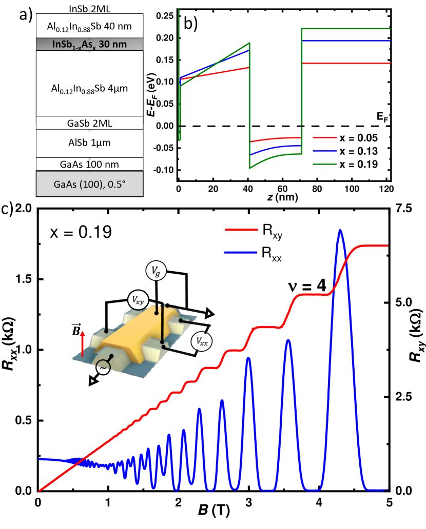
Using a self-consistent Schrödinger-Poisson (SP) simulator (NEXTNANO3 [29]) we calculate the band edge profile for the devices used in our experiments under changing gate potentials. As highlighted in Fig. 1b, in comparison to undoped InSb quantum wells [30, 28], these undoped InSbAs samples have a conductive 2DEG channel in the quantum well at zero gate bias; higher carrier density at = 0 V is obtained with increasing arsenic mole fraction (see Table 1) [31, 11].
Insulated-gate Hall bars were fabricated to study electrical transport properties. Mesas were defined with a citric acid etch. The Hall bars typically are 75 m wide and 1 mm long. The Ohmic probes are separated by 150 m along the mesa edge. Before depositing the Ohmic metal stack an in-situ argon ion mill with a voltage of 250 V, a beam current of 8 mA, and an accelerating voltage of 50 V was performed to etch the top barrier such that the contact metal stack is deposited directly at the InSbAs quantum well. Secondary ion mass spectroscopy was used to determine the position of the quantum well. This milling process was followed by deposition of 20 nm Ti and 180 nm Au for the Ohmic contacts. Next 40 nm of Al2O3 was deposited as a dielectric via atomic layer deposition at 100 ∘C. Finally, the gate electrodes were fabricated with the deposition of 20 nm of Ti and 150 nm Au.
Magnetotransport measurements were performed at temperatures between = 0.3 K and = 10 mK, unless otherwise specified. Higher temperature measurements were required for effective mass determination and investigation of magneto-intersubband scattering. In Fig. 1c we show representative high magnetic field data for Sample C. Well-defined integer quantum Hall states with vanishing longitudinal resistance and quantized Hall resistance are evident. The density calculated from the Hall slope matches the density extracted from analysis of Shubniokov de Haas (SdH) oscillations, indicative of a single conducting channel. We measured mobility as a function of 2DEG density for the three wafers at = 0.3 K to identify the dominant scattering mechanisms and to observe changes that may occur as the arsenic mole fraction is varied between samples. For determination of SOC parameters, our measurements focused on high resolution low magnetic field ( T) measurements of the longitudinal resistance oscillations.
III Results and Discussion
III.1 Electron scattering in ternary InSbAs quantum wells
Scattering of 2D electrons has been thoroughly investigated in the binary compounds InSb [32, 33, 34, 35, 28] and InAs [36, 19]. It was determined that at cryogenic temperatures mobility is primarily limited by long-range Coulomb scattering from remote and background impurities for 2DEG densities below 1 1012 cm-2. Here, we investigate mobility in ternary InSbAs quantum wells. A ternary quantum well may have additional sources of scattering. Anion atoms (Sb, As) will be randomly distributed based on the available sublattice sites, generating short-range disorder [37]. Alloy disorder and interface roughness scattering are sources of short-range scattering that may lower mobility and modify the functional dependence of mobility on 2DEG density in InSbAs channels [38, 39].
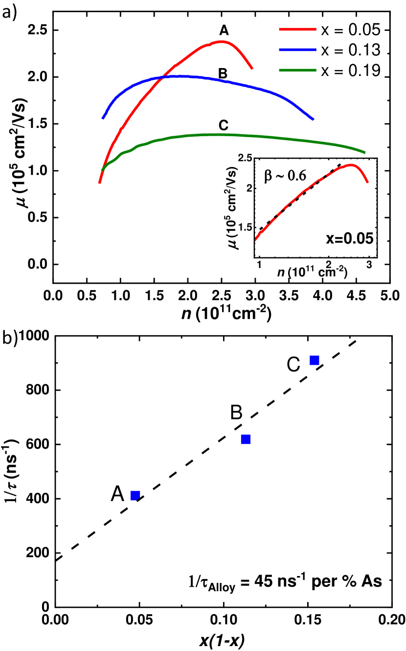
Mobility () vs. 2DEG density measured at =0.3 K for different arsenic mole fractions is displayed in Fig. 2a. As the arsenic mole fraction increases from Sample A to Sample C, a decrease in peak mobility is observed. In addition, a change in the functional dependence of vs. 2DEG density is evident. For Sample A at low density, mobility is a strongly increasing function of density, typical of charged impurity scattering. The dependence may be approximated by over the limited density range of cm-2, yielding an exponent of = 0.6, as seen in the inset of Fig. 2a with data plotted on a log-log scale. = 0.6 indicates that long-range charge disorder dominates scattering in this density regime, specifically Coulomb disorder near the quantum well [39]. In addition to point defects randomly distributed in the vicinity of the quantum well, the semiconductor/dielectric interface is a known source of fixed surface charge. In our structures, this surface is 40 nm away from the quantum well. Below cm-2, the slope in the vs. data increases, suggestive of a transition to a localized regime at lowest density [39].
We note that at a fixed density of 2.5 cm-2, a decrease (increase) in mobility (scattering rate) with increasing arsenic mole fraction is observed, where . Mobility peaks at 2.4 cm2/Vs for Sample A, followed by Sample B and Sample C with mobility of 2.0 cm2/Vs and 1.4 105 cm2/Vs at the same 2DEG density (Table 1). A recent work from Lei [28] reports mobility of 2.6 105 cm2/Vs at density 2.4 cm-2 in an undoped InSb quantum well, a value similar to that seen in Sample A, suggesting that alloy disorder scattering is not yet dominant at .
For Sample B and Sample C, the weaker dependence of mobility on 2DEG density suggests that short-range scattering limits mobility at increased arsenic mole fraction [39]. The progression of vs. from Sample A to B and C indicates that alloy disorder significantly impacts mobility at mole fractions above .
According to Matthiessen’s rule, the total scattering rate () is determined by summing the scattering rates due to all independent scattering mechanisms. At fixed measurement temperature = 0.3 K, we assume that 1/, where includes contributions for all scattering mechanisms other than alloy disorder scattering. The alloy scattering rate should be linear with , where is the As mole fraction, is the effective mass and is the alloy scattering potential [40].
In order to assess the increase in scattering associated with the change in arsenic mole fraction we plot the total scattering rate () vs at = 0.3 K and cm-2 as seen in Fig. 2b. The linear dependence of the total scattering rate with yields a slope of 1/ = 45 ns-1 per As, which quantifies the impact of alloy scattering as we increase arsenic mole fraction.
To the best of our knowledge, the alloy scattering rate in InSbAs quantum wells has not been reported previously. Therefore, we compare the extracted alloy scattering rate of 1/ = 45 ns-1 per As with the alloy scattering rate of ns-1 per As extracted by Gardner et al. in the more widely studied AlxGa1-xAs ternary [41]. The rate measured in InSb1-xAsx quantum wells is comparable to AlxGa1-xAs. is expected to be proportional to and m∗. The alloy scattering potential for an InSb-InAs alloy is theoretically predicted to be 0.82 eV compared to 0.12 eV for GaAs-AlAs alloy [42] while is 0.010-0.019me for InSb1-xAsx ternary compared to 0.067me for AlxGa1-xAs [41]. Therefore, the alloy scattering rate for InSb1-xAsx is within a factor of 2 of AlxGa1-xAs, despite the significantly higher alloy scattering potential, due to the compensatory impact of the lower effective mass.
We performed temperature dependent magnetotransport measurements to extract the values of the effective mass for all samples at a density of 2 1011 cm-2 [43]. Theory and experiments have shown that the ternary InSb1-xAsx has a lower effective mass with increasing arsenic mole fraction [14, 13, 31, 11]. Our analysis yielded results consistent with this trend, as displayed in Table 1.

Finally we note a decrease in mobility for all samples above cm-2, as seen Fig. 2a. Simulations point to the occupation of the second subband at a similar density for all samples, 3 1011 cm-2, as seen in Fig. 3a. The drop in mobility in our data may be attributed to the proximity of the Fermi level to the bottom of the second subband, allowing a channel for intersubband scattering [44]. Another possible contribution is interface roughness scattering, since the electron wavefuncion is pulled closer to the top barrier with higher gate voltage, as seen in the simulation shown in Fig. 3b.
III.2 Analysis of spin-orbit coupling in InSbAs quantum wells
Due to high mobility and small effective mass we are able to resolve beating in the oscillatory longitudinal resistance at low magnetic field. Beating may be driven by several mechanisms, including density inhomogeneity [45], magneto-intersubband scattering [46, 47, 48, 49] or zero-field spin splitting arising from strong spin-orbit coupling [50]. Magnetotransport measurements taken with different contact configurations on our devices indicate that beating does not result from density inhomogeneity. Intersubband scattering may occur when the chemical potential is proximal to the second electric subband. Landau level crossing enhances magneto-intersubband scattering at magnetic field given by [46, 47, 48, 49]. As noted previously, simulations indicate the occupation of the second subband is possible at high 2DEG density, therefore we have measured temperature-dependent magnetotransport to rule out magneto-intersubband scattering.
We first note that the magnetotransport does not show signs of significant parasitic conduction. As shown in Fig. 1b, clear quantum Hall plateaus are resolved with the longitudinal resistance vanishing at 1.8 T. Furthermore, the densities extracted from the Hall slope and from the SdH oscillations minima are equal. This suggests minimal contribution from parallel conduction channels in the investigated range of density, with only the lowest energy subband contributing significantly to transport.
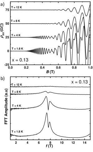
Magneto-intersubband scattering occurs when the Landau levels of two bands cross, causing oscillations in the magnetotransport at frequency . If this value is close to the frequency of the underlying SdH oscillations, beating may result. To understand if this mechanism was active in our devices, measurements of the longitudinal resistance were performed over a broad range of temperature. Magneto-intersubband scattering is relatively insensitive to changes in temperature, whereas damping of the SdH oscillations with temperature occurs rapidly as /sinh with where [49, 48, 27]. We performed temperature dependent measurements for Sample B and Sample C at the highest achievable density. We observe rapid damping of the oscillations (Fig. 4a) with increased temperature, also reflected in the fast Fourier transforms (FFT). The amplitudes of the two frequency peaks clearly decrease with increasing temperature (Fig. 4b), indicating that their origin is SdH oscillations rather than magneto-intersubband scattering.
III.3 Rashba spin-orbit coupling
The beating observed in low-field transport in our samples is attributed to zero field spin-splitting due to strong Rashba spin-orbit coupling. Zero-field spin-splitting () is given by , where is the Fermi wave vector defined as and is the Rashba coupling parameter. The presence of SOC results in beating in the SdH oscillations as seen in Fig. 5. Beating occurs because two occupied spin bands have two slightly different densities of electrons, giving rise to two closely spaced frequencies of SdH oscillations. This allows extraction of from oscillatory low-field transport [51, 52, 21, 23, 53, 19]. Fourier analysis of longitudinal magnetoresistance facilitates extraction of the Rashba parameter as a function of 2DEG density and arsenic mole fraction in our devices.
We assume the Rashba coupling is the major contribution to SOC in our devices. Due to the lack of microscopic inversion symmetry in zinc-blende crystals, the Dresselhaus coupling also contributes to SOC in zinc-blende InSbAs quantum wells [54, 25]. However, Rashba coupling is known to dominate in highly asymmetric quantum wells such as those studied here [55, 20]. The increased electrostatic asymmetry with increased gate voltage is confirmed by self-consistent calculation of the band diagram as shown in Fig. 3b.
The Rashba parameter depends on the electric field in the quantum well and in the top and bottom barriers when the wavefunction has finite value in the barriers. The conduction band discontinuities at the top and bottom interfaces also contribute when the wavefunction has differing amplitude at the top and bottom interfaces [52, 53].
| (1) |
The parametric dependence of is shown in Eq. 1, where the first term is the expectation value of the electric field in the quantum well weighted by , which is a material specific parameter determined by interband matrix elements and energy differences [56]. is expected to increase with increasing arsenic mole fraction in the InSbAs ternaries we study. The second term contains the expectation value of the electric field in the upper and lower barriers weighted by which characterizes Rashba coupling in the barriers. The third term accounts for the contributions from the wavefunction at the upper () and lower interface (), where parameterizes band discontinuity at the interfaces.
The Rashba parameter is determined once , the density difference between the two electron spin bands, is known [52]. This is accomplished by taking a fast Fourier transform of the low-field longitudinal resistance, which yields the frequencies of the two oscillations, and . The Rashba parameter is given by Eq. 2 [52].
| (2) |
In Eq. 2, , and is the effective mass. We use the effective mass values measured for our samples as shown in Table 1.
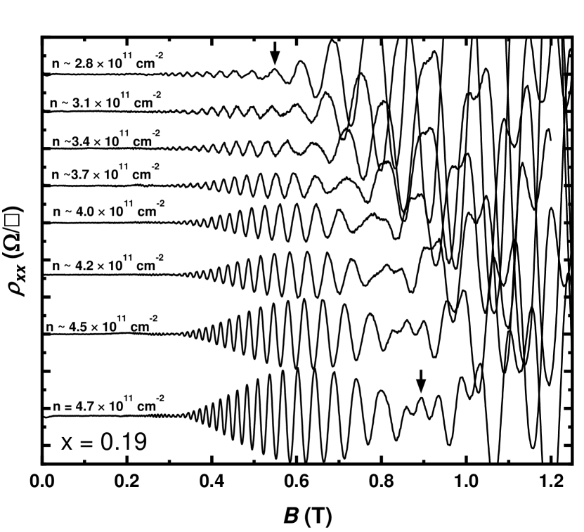
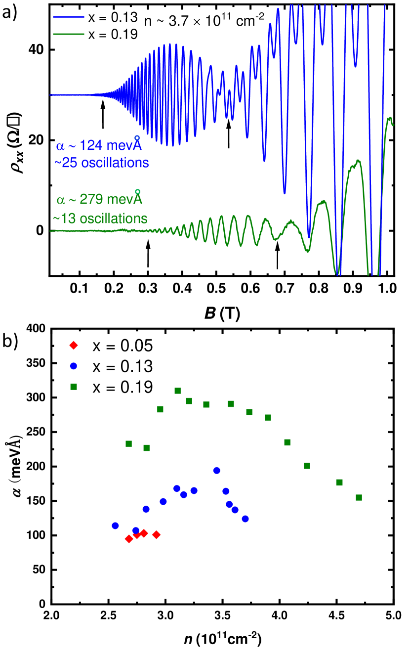
The increase of the Rashba coupling with larger arsenic mole fraction is evident in the raw magneto-resistance data plotted in Fig. 6a. The number of oscillations between two nodes changes from approximately 25 to 13 from = 0.13 to = 0.19. Since the number of oscillations is inversely proportional to , this indicates a higher for the higher arsenic mole fraction sample [21, 50]. The evolution of the Rashba parameter with density for all arsenic mole fractions is depicted in Fig. 6b. A noticeable increase of the Rashba coupling with increased arsenic mole fraction is evident. If we compare the Rashba coupling extracted at the same density, 2.9 1011 cm-2, the values for Sample A to C are respectively 100, 150, 280 meV Å. Because the samples have the same top and bottom barriers, nearly equal electric field in the quantum well and matching electron distributions (as inferred from simulations), the increase in SOC may be attributed to an increase in the material specific Rashba coupling parameter with higher arsenic concentration. This is consistent with predictions [13, 14, 15, 8].
For Sample B and Sample C, the Rashba coupling increases from 2.5 and 3.5 cm-2. This enhancement is consistent with simulations, which indicate an increase in electric field and wavefunction asymmetry towards the top barrier, as also seen in Fig. 2b. However, for both Samples B and C, the Rashba parameter decreases after 3.5 cm-2. It is worth noting that the decrease in occurs at approximately the same density at which the second electric subband begins to be occupied in the numerical simulations, although contribution from a second subband to the magnetotransport is not apparent in the data. From the simulations, the second subband wavefunction penetrates significantly more into the top barrier than the first subband. A possible explanation for the decrease in with higher density is the increased propensity of electrons to reside in the top barrier, which has lower intrinsic SOC than the quantum well. However, more investigation is needed to quantitatively understand this trend.
IV Conclusions
In this work we have detailed the low temperature transport properties of a series of 2DEGs confined in InSbAs quantum wells with different arsenic mole fractions. We extracted an alloy scattering rate of 1/ = 45 ns-1 per As, determined the dependence of mobility on 2DEG density and arsenic mole fraction, and detailed the evolution of dominant scattering mechanisms. Analysis of SdH oscillations enabled extraction of the Rashba coupling strength over a wide range of 2DEG density for all mole fractions. At comparable density and nearly equal electric field, we observed an increase of with arsenic mole fraction. For = 0.19 is 300 meVÅ, one of the highest values reported for III-V heterostructures. These results agree with theoretical predictions of enhancement of SOC with arsenic mole fraction [15, 13, 14] and suggest that InSb1-xAsx 2DEGs are a promising platform for exploration of topological superconductivity by incorporating these ternary quantum wells in a shallow structure coupled to an s-wave superconductor.
Author to whom correspondence should be addressed: mmanfra@purdue.edu
We thank Dr. James Nakamura for suggestions for manuscript improvement and Georg Winkler, Sam Teicher and Fabiano Corsetti for fruitful discussion. This work was supported by Microsoft Quantum.
The data that support the findings of this study are available from the corresponding author upon reasonable request.
The authors have no conflicts to disclose.
References
- Lutchyn et al. [2010] R. M. Lutchyn, J. D. Sau, and S. D. Sarma, Majorana Fermions and a Topological Phase Transition in Semiconductor-Superconductor Heterostructures, Phys. Rev. Lett. 105, 077001 (2010).
- Oreg et al. [2010] Y. Oreg, G. Refael, and F. v. Oppen, Helical Liquids and Majorana Bound States in Quantum Wires, Phys. Rev. Lett. 105, 177002 (2010).
- Shabani et al. [2016] J. Shabani, M. Kjaergaard, H. J. Suominen, Y. Kim, F. Nichele, K. Pakrouski, T. Stankevic, R. M. Lutchyn, P. Krogstrup, R. Feidenhans’l, S. Kraemer, C. Nayak, M. Troyer, C. M. Marcus, and C. J. Palmstrøm, Two-dimensional epitaxial superconductor-semiconductor heterostructures: A platform for topological superconducting networks, Phys. Rev. B 93, 155402 (2016).
- Kjaergaard et al. [2016] M. Kjaergaard, F. Nichele, H. J. Suominen, M. P. Nowak, M. Wimmer, A. R. Akhmerov, J. A. Folk, K. Flensberg, J. Shabani, C. J. Palmstrøm, and C. M. Marcus, Quantized conductance doubling and hard gap in a two-dimensional semiconductor–superconductor heterostructure, Nature Communications 7, 12841 (2016).
- Drachmann et al. [2017] A. C. C. Drachmann, H. J. Suominen, M. Kjaergaard, B. Shojaei, C. J. Palmstrøm, C. M. Marcus, and F. Nichele, Proximity Effect Transfer from NbTi into a Semiconductor Heterostructure via Epitaxial Aluminum, Nano Lett. 17, 1200 (2017).
- Ke et al. [2019] C. T. Ke, C. M. Moehle, F. K. de Vries, C. Thomas, S. Metti, C. R. Guinn, R. Kallaher, M. Lodari, G. Scappucci, T. Wang, R. E. Diaz, G. C. Gardner, M. J. Manfra, and S. Goswami, Ballistic superconductivity and tunable –junctions in InSb quantum wells, Nature Communications 10, 3764 (2019).
- Fornieri et al. [2019] A. Fornieri, A. M. Whiticar, F. Setiawan, E. Portolés, A. C. Drachmann, A. Keselman, S. Gronin, C. Thomas, T. Wang, R. Kallaher, et al., Evidence of topological superconductivity in planar Josephson junctions, Nature 569, 89 (2019).
- Mayer et al. [2020] W. Mayer, W. F. Schiela, J. Yuan, M. Hatefipour, W. L. Sarney, S. P. Svensson, A. C. Leff, T. Campos, K. S. Wickramasinghe, Dartiailh, et al., Superconducting proximity effect in InAsSb surface quantum wells with in situ al contacts, ACS Appl. Electron. Mater. 2, 2351 (2020).
- Dartiailh et al. [2021a] M. C. Dartiailh, J. J. Cuozzo, B. H. Elfeky, W. Mayer, J. Yuan, K. S. Wickramasinghe, E. Rossi, and J. Shabani, Missing Shapiro steps in topologically trivial Josephson junction on InAs quantum well, Nature Communications 12, 78 (2021a).
- Dartiailh et al. [2021b] M. C. Dartiailh, W. Mayer, J. Yuan, K. S. Wickramasinghe, A. Matos-Abiague, I. Žutić, and J. Shabani, Phase Signature of Topological Transition in Josephson Junctions, Phys. Rev. Lett. 126, 036802 (2021b).
- Moehle et al. [2021] C. M. Moehle, C. T. Ke, Q. Wang, C. Thomas, D. Xiao, S. Karwal, M. Lodari, V. van de Kerkhof, R. Termaat, G. C. Gardner, G. Scappucci, M. J. Manfra, and S. Goswami, InSbAs two-dimensional electron gases as a platform for topological superconductivity, Nano Lett. 21, 9990 (2021).
- Datta and Das [1990] S. Datta and B. Das, Electronic analog of the electro-optic modulator, App. Phys. Lett. 56, 665 (1990).
- Berolo et al. [1973] O. Berolo, J. C. Woolley, and J. A. Van Vechten, Effect of disorder on the conduction-band effective mass, valence-band spin-orbit splitting, and the direct band gap in III-V alloys, Phys. Rev. B 8, 3794 (1973).
- Bouarissa and Aourag [1999] N. Bouarissa and H. Aourag, Effective masses of electrons and heavy holes in InAs, InSb, GaSb, GaAs and some of their ternary compounds, Infrared Physics and Technology 40, 343 (1999).
- Winkler et al. [2016] G. W. Winkler, Q. Wu, M. Troyer, P. Krogstrup, and A. A. Soluyanov, Topological Phases in InAs1-xSbx: From Novel Topological Semimetal to Majorana Wire, Phys. Rev. Lett. 117, 076403 (2016).
- Sestoft et al. [2018] J. E. Sestoft, T. Kanne, A. N. Gejl, M. Von Soosten, J. S. Yodh, D. Sherman, B. Tarasinski, M. Wimmer, E. Johnson, M. Deng, J. Nygård, T. S. Jespersen, C. M. Marcus, and P. Krogstrup, Engineering hybrid epitaxial InAsSbAl nanowires for stronger topological protection, Phys. Rev. Materials 2, 044202 (2018).
- Dresselhaus [1955] G. Dresselhaus, Spin-orbit coupling effects in zinc blende structures, Phys. Rev. 100, 580 (1955).
- Bychkov and Rashba [1984] Y. A. Bychkov and E. I. Rashba, Oscillatory effects and the magnetic susceptibility of carriers in inversion layers, J. Phys C: Solid State Phys. 17, 6039 (1984).
- Hatke et al. [2017] A. T. Hatke, T. Wang, C. Thomas, G. C. Gardner, and M. J. Manfra, Mobility in excess of 106 cm2/Vs in InAs quantum wells grown on lattice mismatched InP substrates, Appl. Phys. Lett. 111, 142106 (2017).
- Gilbertson et al. [2009] A. M. Gilbertson, W. R. Branford, M. Fearn, L. Buckle, P. D. Buckle, T. Ashley, and L. F. Cohen, Zero-field spin splitting and spin-dependent broadening in high-mobility asymmetric quantum well heterostructures, Phys. Rev. B 79, 235333 (2009).
- Nitta et al. [1997] J. Nitta, T. Akazaki, H. Takayanagi, and T. Enoki, Gate control of spin-orbit interaction in an inverted In0.53Ga0.47AsIn0.52Al0.48As heterostructure, Phys. Rev. Lett. 78, 1335 (1997).
- Luo et al. [1990] J. Luo, H. Munekata, F. F. Fang, and P. J. Stiles, Effects of inversion asymmetry on electron energy band structures in quantum wells, Phys. Rev. B 41, 7685 (1990).
- Heida et al. [1998] J. Heida, B. van Wees, J. Kuipers, T. Klapwijk, and G. Borghs, Spin-orbit interaction in a two-dimensional electron gas in a InAsAlSb quantum well with gate-controlled electron density, Phys. Rev. B 57, 11911 (1998).
- Kim et al. [2010] K.-H. Kim, H.-J. Kim, H. C. Koo, J. Chang, and S.-H. Han, Spin-Orbit coupling in double-sided dopes InAs quantum well structures, Appl. Phys. Lett 97, 012504 (2010).
- Kallaher et al. [2010] R. L. Kallaher, J. J. Heremans, N. Goel, S. J. Chung, and M. B. Santos, Spin-orbit interaction determined by antilocalization in an InSb quantum well, Phys. Rev. B 81, 075303 (2010).
- Lee et al. [2011] T. Y. Lee, J. Chang, M. C. Hickey, H. C. Koo, H.-J. Kim, S. H. Han, and J. S. Moodera, Quantum well thickness dependence of Rashba spin–orbit coupling in the InAsInGaAs heterostructure, Appl. Phys. Lett 98, 202504 (2011).
- Shojaei et al. [2016] B. Shojaei, P. J. J. O’malley, J. Shabani, P. Roushan, B. D. Schultz, R. M. Lutchyn, C. Nayak, J. M. Martinis, and C. J. Palmstrøm, Demonstration of gate control of spin splitting in a high-mobility InAsAlSb two-dimensional electron gas, Phys. Rev. B 93, 75302 (2016).
- Lei et al. [2022] Z. Lei, E. Cheah, K. Rubi, M. E. Bal, C. Adam, R. Schott, U. Zeitler, W. Wegscheider, T. Ihn, and K. Ensslin, High-quality two-dimensional electron gas in undoped InSb quantum wells, Phys. Rev. Research 4, 013039 (2022).
- Birner et al. [2007] S. Birner, T. Zibold, T. Andlauer, T. Kubis, M. Sabathil, A. Trellakis, and P. Vogl, nextnano: General purpose 3-D simulations, IEEE Trans. Electron Dev 54, 2137 (2007).
- Kulesh et al. [2020] I. Kulesh, C. T. Ke, C. Thomas, S. Karwal, C. M. Moehle, S. Metti, R. Kallaher, G. C. Gardner, M. J. Manfra, and S. Goswami, Quantum dots in an InSb two-dimensional electron gas, Phys. Rev. Applied 13, 041003 (2020).
- Suchalkin et al. [2016] S. Suchalkin, J. Ludwig, G. Belenky, B. Laikhtman, G. Kipshidze, Y. Lin, L. Shterengas, D. Smirnov, S. Luryi, W. L. Sarney, and S. P. Svensson, Electronic properties of unstrained unrelaxed narrow gap alloys, J. Phys. D: Appl. Phys. 49, 105101 (2016).
- Chung et al. [1999] S. J. Chung, K. J. Goldammer, S. C. Lindstrom, M. B. Johnson, and M. B. Santos, Study of factors limiting electron mobility in InSb quantum wells, Journal of Vacuum Science and Technology B: Microelectronics and Nanometer Structures Processing, Measurement, and Phenomena 17, 1151 (1999).
- Yi et al. [2015] W. Yi, A. A. Kiselev, J. Thorp, R. Noah, B.-m. Nguyen, S. Bui, R. D. Rajavel, T. Hussain, M. F. Gyure, P. Kratz, Q. Qian, M. J. Manfra, V. S. Pribiag, L. P. Kouwenhoven, C. M. Marcus, M. Sokolich, W. Yi, A. A. Kiselev, J. Thorp, R. Noah, B.-m. Nguyen, S. Bui, R. D. Rajavel, T. Hussain, M. F. Gyure, P. Kratz, Q. Qian, M. J. Manfra, V. S. Pribiag, L. P. Kouwenhoven, and C. M. Marcus, Gate-tunable high mobility remote-doped InSb/ quantum well heterostructures, Appl. Phys. Lett. 106, 142103 (2015).
- Pooley et al. [2010] O. Pooley, A. Gilbertson, P. D. Buckle, R. Hall, M. Emeny, M. Fearn, M. Halsall, L. Cohen, and T. Ashley, Quantum well mobility and the effect of gate dielectrics in remote doped InSbAlxIn1-xSb heterostructures, Semicond. Sci. Technol. 25, 125005 (2010).
- Lehner et al. [2018] C. A. Lehner, T. Tschirky, T. Ihn, W. Dietsche, J. Keller, S. Fält, and W. Wegscheider, Limiting scattering processes in high-mobility InSb quantum wells grown on GaSb buffer systems, Phys. Rev. Materials 2, 054601 (2018).
- Shabani et al. [2014] J. Shabani, A. P. McFadden, B. Shojaei, and C. J. Palmstrøm, Gating of high-mobility InAs metamorphic heterostructures, Appl. Phys. Lett. 105, 262105 (2014).
- Harrison and Hauser [1976] J. Harrison and J. Hauser, Alloy scattering in ternary III-V compounds, Phys. Rev. B 13, 5347 (1976).
- Chin et al. [1991] V. W. Chin, R. Egan, and T. Tansley, Electron mobility in InAs1-xSbx and the effect of alloy scattering, J. Appl. Phys. 69, 3571 (1991).
- Das Sarma and Hwang [2013] S. Das Sarma and E. H. Hwang, Universal density scaling of disorder-limited low-temperature conductivity in high-mobility two-dimensional systems, Phys. Rev. B 88, 035439 (2013).
- Bastard [1991] G. Bastard, Wave mechanics applied to semiconductor heterostructures (New York,Wiley-Interscience, 1991).
- Gardner et al. [2013] G. C. Gardner, J. D. Watson, S. Mondal, N. Deng, G. A. Csáthy, and M. J. Manfra, Growth and electrical characterization of /as/ modulation-doped quantum wells with extremely low x, App. Phys. Lett. 102, 252103 (2013).
- Ferry [1978] D. K. Ferry, Alloy Scattering in ternary III-V compound, Phys. Rev. B 17, 912 (1978).
- Ihn [2009] T. Ihn, Semiconductor Nanostructures: Quantum states and electronic transport (OUP Oxford, 2009).
- Fletcher et al. [1988] R. Fletcher, E. Zaremba, M. O’iorio, C. T. Foxon, and J. J. Harris, Evidence of a mobility edge in the second subband of an Al0.33Ga0.67As-GaAs heterojunction, Phys. Rev. B 38, 7866(R) (1988).
- Brosig et al. [1999] S. Brosig, K. Ensslin, R. J. Warburton, C. Nguyen, B. Brar, M. Thomas, and H. Kroemer, Zero-field spin splitting in quantum wells revisited, Phys. Rev. B 60, R13989(R) (1999).
- Leadley et al. [1992] D. Leadley, R. Fletcher, R. Nicholas, F. Tao, C. Foxon, and J. Harris, Intersubband resonant scattering in GaAs-Ga1-xAlxAs heterojunctions, Phys. Rev. B 46, 12439 (1992).
- Raikh and Shahbazyan [1994] M. E. Raikh and T. V. Shahbazyan, Magnetointersubband oscillations of conductivity in a two-dimensional electronic system, Phys. Rev. B 49, 5531 (1994).
- Sander et al. [1998] T. H. Sander, S. N. Holmes, J. J. Harris, D. K. Maude, and J. C. Portal, Determination of the phase of magneto-intersubband scattering oscillations in heterojunctions and quantum wells, Phys. Rev. B 58, 13856 (1998).
- Rowe et al. [2001] A. C. H. Rowe, J. Nehls, R. A. Stradling, and R. S. Ferguson, Origin of beat patterns in the quantum magnetoresistance of gated InAsGaSb and InAsAlSb quantum wells, Phys. Rev. B 63, 201307 (R) (2001).
- Luo et al. [1988] J. Luo, H. Munekata, F. F. Fang, and P. J. Stiles, Observation of the zero-field spin splitting of the ground electron subband in quantum wells, Phys. Rev. B 38, 10142(R) (1988).
- Das et al. [1989] B. Das, D. C. Miller, S. Datta, R. Reifenberger, W. P. Hong, P. K. Bhattacharya, J. Singh, and M. Jaffe, Evidence for spin splitting in InxGa1-xAsIn0.52Al0.48As heterostructures as B0, Phys. Rev. B 39, 1411(R) (1989).
- Engels et al. [1997] G. Engels, J. Lange, T. Schäpers, and H. Lüth, Experimental and theoretical approach to spin splitting in modulation-doped InxGa1-xAs InP quantum wells for B0, Phys. Rev. B 55, R1958(R) (1997).
- Schäpers et al. [1998] T. Schäpers, G. Engels, J. Lange, T. Klocke, M. Hollfelder, and H. Lüth, Effect of the heterointerface on the spin splitting in modulation doped InxGa1-xAsInP quantum wells for B→0, J. Appl. Phys. 83, 4324 (1998).
- Nishizako et al. [2010] N. Nishizako, T. Manago, S. Ishida, H. Geka, and I. Shibasaki, Carrier density dependence of spin-orbit interaction in InAsSb quantum wells, Physica E: Low-dimensional Systems and Nanostructures 42, 975 (2010).
- Khodaparast et al. [2004] G. A. Khodaparast, R. E. Doezema, S. J. Chung, K. J. Goldammer, and M. B. Santos, Spectroscopy of Rashba spin splitting in InSb quantum wells, Phys. Rev. B 70, 155322 (2004).
- Winkler [2003] R. Winkler, Spin-orbit coupling effects in two-dimensional electron and hole systems, Vol. 191 (Springer, 2003).