Two New CNTFET Quaternary Full Adders for Carry-Propagate Adders
Abstract
In Carry Propagate Adders, carry propagation is the critical delay. For the 1-digit adders that they use, the most efficient scheme is to generate two intermediate carries: Cout0 (=0) and (=1). Then multiplex them to produce the correct output according to . For any radix, the carry output has always a logical value 0 or 1. We show that using 0 and levels for input and output carries instead of 0 and /3 in quaternary full adders significantly reduce the carry propagation. We compare such a quaternary full adder with binary full adders to implement N-digit carry propagate adders.
Index Terms:
Quaternary adders, Binary adders, Carry-Propagate Adders, CNTFET, propagation delays, power dissipation, chip area.I Introduction
Carry Propagate Adders (CPAs) are the most simple N-digit adders. Fig.1 presents a 4-digit CPA. In this paper, we consider quaternary CPAs. From Fig.1, it results that the performance of a CPA is a direct function of the used 1-digit full adder. More precisely, the critical delay path of CPA is related to the carry propagation. Several quaternary full adders with CNTFET simulations have been published in the last decade [1, 2, 3]. The truth table of the quaternary full adder is shown in Table I. So, quaternary 1-digit full adders have quaternary inputs and outputs logical values 0,1,2,3 (corresponding to 0,/3, 2*/3, ) and carry logical values 0,1 (corresponding generally to /3).

| A | B | Ci | QS | QC | A | B | Ci | QS | QC | |
|---|---|---|---|---|---|---|---|---|---|---|
| 0 | 0 | 0 | 0 | 0 | 0 | 0 | 1 | 1 | 0 | |
| 0 | 1 | 0 | 1 | 0 | 0 | 1 | 1 | 2 | 0 | |
| 0 | 2 | 0 | 2 | 0 | 0 | 2 | 1 | 3 | 0 | |
| 0 | 3 | 0 | 3 | 0 | 0 | 3 | 1 | 0 | 1 | |
| 1 | 0 | 0 | 1 | 0 | 1 | 0 | 1 | 2 | 0 | |
| 1 | 1 | 0 | 2 | 0 | 1 | 1 | 1 | 3 | 0 | |
| 1 | 2 | 0 | 3 | 0 | 1 | 2 | 1 | 0 | 1 | |
| 1 | 3 | 0 | 0 | 1 | 1 | 3 | 1 | 1 | 1 | |
| 2 | 0 | 0 | 2 | 0 | 2 | 0 | 1 | 3 | 0 | |
| 2 | 1 | 0 | 3 | 0 | 2 | 1 | 1 | 0 | 1 | |
| 2 | 2 | 0 | 0 | 1 | 2 | 2 | 1 | 1 | 1 | |
| 2 | 3 | 0 | 1 | 1 | 2 | 3 | 1 | 2 | 1 | |
| 3 | 0 | 0 | 3 | 0 | 3 | 0 | 1 | 0 | 1 | |
| 3 | 1 | 0 | 0 | 1 | 3 | 1 | 1 | 1 | 1 | |
| 3 | 2 | 0 | 1 | 1 | 3 | 2 | 1 | 2 | 1 | |
| 3 | 3 | 0 | 2 | 1 | 3 | 3 | 1 | 3 | 1 |
There are two techniques to get 0, 1, 2 and 3 values. The first one uses three power supplies , /3 and /3. The second one uses only one power supply () and get the intermediate values through transistors connected as resistors. In that case, there is a large static power dissipation resulting from the direct current flow through the voltage divider. This is why we only consider the option with three power supplies.
The best implementation of ternary adders uses the multiplexer approach [4]. Similarly, the best implementation to date of quaternary adders (QFAs) [3] uses this approach. Our implementations are a variant of the QFA proposed in [3]. With this approach, all proposed designs use /3 as the voltage when carry=1. This raises one question : do the binary carries must mandatory use 0 and 1 quaternary values or can they use 0 and 3 quaternary values ? In other words, 0 and or 0 and when the quaternary adders have a power supply. In this paper, we consider both cases: QFA1 with carry swing and QFA2 with carry swing.
The paper is organized as follow: First, we present the methodology. Then we present two versions QFA1 and QFA2 that uses the MUX-based approach. Then, we present different 2-bit binary full adders that compute the same amount of information. Finally, we compare the performance of the quaternary and binary full adders and conclude.
The main contributions of this paper are the following one:
-
•
We present two versions of a quaternary adders that minimize the carry propagation. With power supply, the first one has /3 carry swing and the second one carry swing. The second one has smaller carry delays
-
•
The two quaternary adders are compared with 2-bit binary ones. Binary adders can use smaller power supplies (such as /2) to reduce power dissipation
-
•
For most features, the 2-bit binary adders are more efficient than the quaternary ones
II Methodology
The significant figures to compare circuit designs include switching times, power dissipation, chip area, etc. The comparison is realized by using HSpice simulations and evaluating the chip area according to transistor diameters. All simulations are done with the 32nm CNTFET parameters of Stanford library [5]. We use this technology and these parameters as they are used in most papers presenting ternary or quaternary implementations of adders or multipliers.
Generally, propagation delays are presented as an average of the delays corresponding to all combinations of input transitions. This presentation is confusing. For the CPA presented in Fig.1, , (with i=0,1,2,3) and inputs are simultaneously available. The important information is the propagation delay corresponding to the critical paths. For the 4-digit CPA (Fig.1), this critical path is from C0 or or (worst case) then from then from and finally from or (worst case). We will only present the propagation delays corresponding to the critical paths.
Both power and PDP (Power Delay Product) dissipation directly depend on the duration of the input signals. It is important to use the same input signals for all simulations.
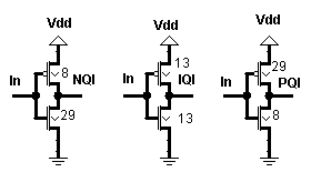
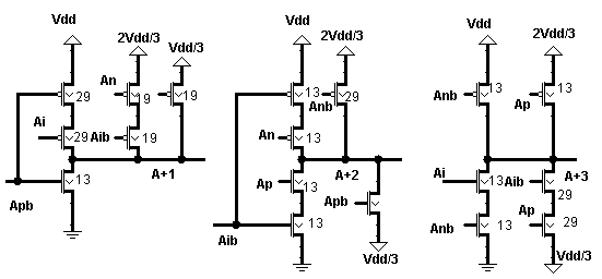
We use a rough evaluation of the chip area by summing the diameters of all the used transistors by each circuit. In this paper, we use the diameter values presented in Table II. The choice of appropriate diameter values is mandatory for the threshold detectors and A¹, A², A³ circuits presented in III-A. Some other values are needed to provide sufficient fan-out to the quaternary multiplexers.
Many techniques have been proposed to design full adders. We only consider techniques with the following properties:
-
•
No static power dissipation.
-
•
The circuit outputs have full swing.
-
•
The circuits should have a sufficient driving capability.
| n | 8 | 10 | 13 | 19 | 29 | 37 |
|---|---|---|---|---|---|---|
| D (nm) | 0.626 | 0.783 | 1.017 | 1.487 | 2.270 | 2.896 |
III New Quaternary Full Adders
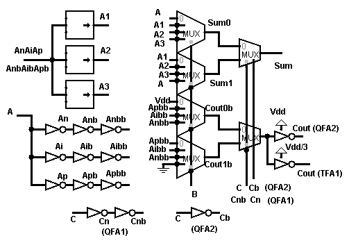
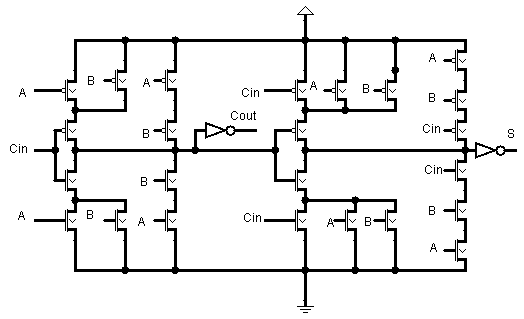
The common scheme is presented in Fig. 2. The two QFAs only differ by the carry operation. Carry input and output values are 0, (QFA1) and 0, (QFA2). The control of the two MUX2 is shown is Fig. 2. The carry out is obtained by inverters with supply (QFA1) or supply (QFA2)
III-A Quaternary Adder Implementation
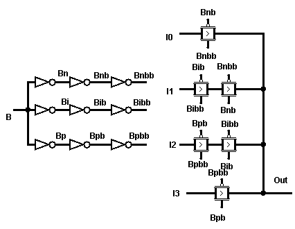
The common functional scheme is shown in Fig. 2. The threshold detectors (Fig. 3), the circuits A¹, A², A³ (Fig. 4) and the MUX4 (Fig. 5) are similar to those presented in [3]. The two final multiplexers are typical binary multiplexers. is computed from and . A final inverter delivers . 4-input multiplexers with quaternary control are used (Fig. 5). The three inverters with outputs , and are also buffers because inverters and have poor driving capability. Paper [3] first uses a quaternary half adder (sum and carry circuits). A second stage computes the final result by adding +1 mod(4) to sum when =1 and computing according to . We directly computes Sum and within a single stage. to propagation delay is reduced to a MUX2 and final inverter path.
III-B Performance
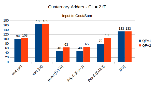
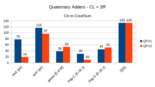
For all simulations, the same input waveforms are used. Extensive simulations have determined that 012321 0 for input a with =0 lead to the input to /Sum worst case delays. Similarly, 01(QFA1) or 3(QFA2) 0 with A=2 and B=1 lead to the to /Sum worst case delays. These configurations are used to evaluate the performance of QFA1 and QFA2. The only difference is the amplitude of the carry swing. The performance results are presented in Fig. 6 and 7. These figures provide the data and allows a direct comparison for each feature. The significant information is Input to (first adder of a CPA), to (following adders) and to Sum (last adder of a CPA). Only simulation results with CL = 2fF are presented.
QFA1 and QFA2 have simular . QFA1 has a small advantage in term of power. However, it is outperformed by QFA2 for to delay, which is the critical delay for a CPA. The situation is the same for PDP. This big advantage comes from the last carry inverter that is more efficient with a supply than with a supply.
IV Binary Full Adders
For comparison, we use two different binary full adders. The first one (BFA1) is the typical 28 T binary full adder (Fig. 8). The second one (BFA2) is shown in Fig. 9. It uses 14 transistors. The two binary full adders operate with the same =0.9V as the quaternary adder. They can also operate with =0.45V, which roughly divide by 4 the dynamic power dissipation. =0.45V is a too small power supply value to operate with the four levels of a quaternary adder.
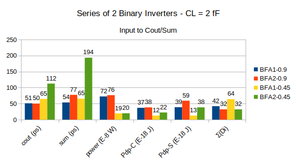
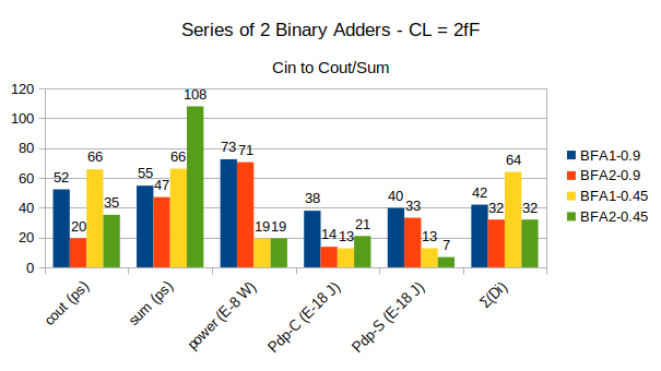
We simulate a series of two binary adders with = 0.9V and = 0.45V to be compared to the quaternary adder. Only simulation results with CL = 2fF are presented. The performance for Input to /Sum with CL = 2fF are given in Fig 10. The performance for to /Sum with CL = 2fF are given in Fig 11.
V Overall comparison
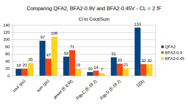
We compare QFA2 (best QFA) with the two versions of BFA2 (best BFA). The data provided in this paper allow the other comparisons.
Fig. 12 presents the comparison results for Input to /Sum. For the only significant delay (Input to ), the two versions of the binary adder have better performance. Fig. 11 present the comparison results for to /Sum. The quaternary adder has a small advantage for to (only one stage versus two for the binary ones) and for power versus BFA-0.9V. However, BFA-0.45V is better in terms of power and PDP. The quaternary adder has a huge disadvantage versus BFA2 in terms of with a x4 ratio. 43% of comes from MUX4s and MUX2s.
As the comparison between quaternary and binary circuits are done with the same technology, there are few opportunities to get different results in the comparisons for different capacitive loads and different temperatures.

VI Concluding remarks
The best implementation of quaternary full adders should minimize the to propagation delay. We have presented two versions of a quaternary full adder for which the to delay is reduced to the path through one MUX2 and one inverter. The first one has the typical 0 and /3 carry levels while the second one uses a carry swing. For CPAs, the QFA2 version is more efficient.
We have compared the new quaternary adders with two binary adders. For carry propagation and power, QFA2 is better than BFA2 using the same 0.9V power supply. BFA2 with 0.45V power supply has a significant advantage in terms of power and PDP. The quaternary full adder uses far more chip area. It mainly comes from the needed MUX4 circuits. Inverters used as buffers are also needed to overcome the driving capability weakness of the QN and QP circuits.
CPAs are circuits for which moving from binary to quaternary N-digit CPAs is simple: just replace the binary full adders by quaternary full adders. They are among the most favorable circuits for the quaternary approach. Moving from a 2N*2N-bit binary multiplier to a N*N digit quaternary multiplier is not so simple as quaternary multipliers uses both quaternary 1-digit adders and 1-digit multipliers.
References
- [1] S.A. Ebrahimi,M.R. Reshadinezhad, A. Bohlooli, M. Shahsavari, “Efficient CNTFET-based design of quaternary logic gates and arithmetic circuits”, Microelectronics Journal, pp 156-166, January 2016
- [2] M.H. Moaiyeri, K. Navi, O. Hashemipour, “Design and Evaluation of CNFET-Based Quaternary Circuits”, Circuits Syst Signal Process (2012) 31:1631–1652, DOI 10.1007/s00034-012-9413-2
- [3] E. Roosta and S. A. Hosseiny, “A Novel Multiplexer-Based Quaternary Full Adder in Nanoelectronics”, Circuits, Systems and Signal Processing, https://doi.org/10.1007/s00034-019-01039-8
- [4] J. M. Aljaam, R. A. Jaber and S. A. Al-Maadeed, ”Novel Ternary Adder and Multiplier Designs Without Using Decoders or Encoders,” in IEEE Access, vol. 9, pp. 56726-56735, 2021, doi: 10.1109/ACCESS.2021.3072567.
- [5] J. Deng and H. P. Wong, ”A Compact SPICE Model for Carbon-Nanotube Field-Effect Transistors Including Nonidealities and Its Application—Part II: Full Device Model and Circuit Performance Benchmarking,” in IEEE Transactions on Electron Devices, vol. 54, no. 12, pp. 3195-3205, Dec. 2007. https://doi.org/10.1109/TED.2007.909043.