An Atomistic Modelling Framework for Valence Change Memory Cells
Abstract
We present a framework dedicated to modelling the resistive switching operation of Valence Change Memory (VCM) cells. The method combines an atomistic description of the device structure, a Kinetic Monte Carlo (KMC) model for the creation and diffusion of oxygen vacancies in the central oxide under an external field, and an ab initio quantum transport method to calculate electrical current and conductance. As such, it reproduces a realistically stochastic device operation and its impact on the resulting conductance. We demonstrate this framework by simulating a switching cycle for a TiN/HfO2/TiN VCM cell, and see a clear current hysteresis between high/low resistance states, with a conductance ratio of one order of magnitude. Additionally, we observe that the changes in conductance originate from the creation and recombination of vacancies near the active electrode, effectively modulating a tunnelling gap for the current. This framework can be used to further investigate the mechanisms behind resistive switching at an atomistic scale and optimize VCM material stacks and geometries.
keywords:
Valence Change Memory, RRAM , memristors , dielectric breakdown , Kinetic Monte Carlo , quantum transport1 Introduction
Neuromorphic computing units require the development of solid-state synapses that are often realized in the form of devices with adjustable electrical conductance. Amongst such devices are valence change memory (VCM) cells. These are two-terminal metal-oxide-metal stacks across which applied voltages can drive the creation of oxygen vacancies and their redistribution into a conductive filament - an applied voltage of the opposite polarity can then partially dissolve the filament, thus breaking the conductive pathway across the oxide. The resulting conductance can then be measured with a low readout voltage without further disrupting the defect arrangement. VCMs are both relatively straightforward to fabricate and exhibit an especially large dynamic range.
Simulation of these devices is complicated by the stochasticity of their operation and the atomistic granularity of the resulting conductance. The movement of oxygen vacancies has been modelled using Kinetic Monte Carlo (KMC) methods [1, 2] or Molecular Dynamics (MD) simulations [3], and the microscopic nature of bonding across the defective interfaces of a VCM filament has been investigated at the ab initio level [4]. Previous simulation frameworks which attempt to describe the full device-level operation of VCM typically combine these methods with trap-assisted tunneling models of current flow [1, 5, 6]. However, the required equations are derived for single trap energies, and may not fully describe transport through the inhomogeneous defect distribution in a VCM. Capturing both atomic rearrangement and realistic transport properties necessitates a more fundamental level of theory.
Here we present a framework dedicated to modelling VCM. Our method relies on a stochastic Kinetic Monte Carlo (KMC) model parameterized with density functional theory (DFT), followed by ab initio quantum transport simulations, all of which are preformed on the same atomic grid. It thus captures the growth and dissolution of oxygen vacancy filaments through the VCM cell and the electrical current that flows through them.
2 Modelling Framework
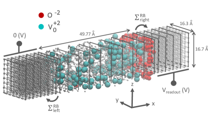
Figure 1 shows a schematic of the nominal VCM cell considered: an amorphous HfO2 oxide with TiN electrodes. The amorphous oxide is initially generated by melting and cooling it from the monoclinic phase using MD. In this process a block of monoclinic HfO2 is first melted at 3000 K for 300 ps, then cooled to 300 K at a rate of 9 K/ps, and finally annealed for 50 ps, all performed under an NVT thermostat with the LAMMPS code [7]. The atomic interactions during this process are characterized by a ReaxFF force-field for Hf-O systems [8]. The purpose behind this MD step is to generate a realistically randomized starting structure; to remove any remaining coordination defects and unrealistic bond lengths, the cell size and atomic positions of the annealed structure are relaxed using the cp2k DFT code [9]. TiN electrodes are then attached along the transport direction. The interface distance between TiN and HfO2 is optimized in cp2k to provide the lowest energy.
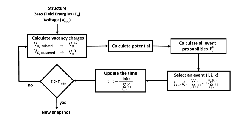
Next, oxygen vacancy () and ion () rearrangements under an applied voltage () are modelled with an in-house KMC code. KMC has been used previously to model physical processes governed by the harmonic transition state theory [10], and is capable of reproducing realistically stochastic behavior [11]. The inputs to this model are a selected set of events which can occur in the oxide, as well as the corresponding activation energies which would need to be overcome to execute them. Here we consider four types of events: (1) vacancy/ion pair generation, (2) vacancy/ion pair recombination, (3) vacancy diffusion (in which a vacancy exchanges lattice positions with an oxygen atom), and (4) oxygen ion diffusion (in which an oxygen ion moves between interstitial sites in the lattice). An event is then selected from this set once per timestep. The selection probability of event ‘x’ occuring between locations (or ‘sites’) ‘’ and ‘’ in the oxide is given by
| (1) |
where is the zero-field activation energy of event x, and is an attempt frequency [2]. The sites involved in each event are restricted to being within a predefined neighbor radius of one another. The zero-field activation energies are found for amorphous HfO2 through DFT calculations, using the Nudged Elastic Band (NEB) method. We assume a reduced activation energy for vacancy generation at the interface with the active (top) electrode [12]. Subtracted from this is the energy provided by the applied field , considering the charge () and potential () for each pair of sites involved. Clustered vacancies are presumed conductive and first set to a charge state of zero (). at each site is then determined by treating the oxide as a network of nodes across which dissipates.
The KMC algorithm makes a list whose elements correspond to the cumulative sum of event probabilities , and chooses the first element of the list that is greater than the sum of all event probabilities , multiplied by a random number , . The corresponding event is thus chosen to occur. The event selection-and-execution process repeats until the simulation timescale reaches the intended duration for which is applied. A device snapshot is finally generated, containing information on the atomic species and positions. Figure 2 presents an overview of this model.
To calculate the conductance of each snapshot, we use the Quantum Transmitting Boundary Method (QTBM) as implemented in the OMEN code [13, 14]. Coherent transport occurs through states , which are found by solving:
| (2) |
Here, describes carrier injection from the contacts, which are coupled to the device through . and are the Hamiltonian and overlap matrices, respectively, as produced with cp2k for each of the KMC snapshots. Due to the localized nature of the underlying Gaussian-type orbitals, and have a block-structure representing atomic layers as pictured in Fig. 1. The ions are not included in electronic structure calculations.
3 Results
We apply this model to simulate the operation of a TiN/HfO2/TiN VCM cell. The HfO2 oxide has a cross-section of 1.67 x 1.63 , for a total of 2252 atoms. Starting from a structure with a formed filament (Fig. 3a), a of -2 V is applied to switch to the high resistance state (HRS, Fig. 3b). = 5 V is then applied to the HRS to recover a low resistance state (LRS, Fig. 3c). In each case, the duration of is 10 ms.
During the transition from the initial structure in Fig. 3a to the HRS in Fig. 3b, recombination of oxygen ions with vacancies near the active electrode results in a local dissolution of the filament, creating a tunneling gap. A transition back to the LRS in Fig. 3c occurs when a sufficiently high regenerates vacancy/ion pairs in this gap. Figure 4a shows the potential for the HRS and LRS structures, as used during the KMC process. The steeper electric potential across the tunneling gap in the HRS increases the likelihood of vacancy regeneration in this area, assisting in the HRS-to-LRS transition. The difference in the transmission function between these two states is pictured in Fig. 4b, and is highest near the conduction band of HfO2, consistent with the location of vacancy defect states at this energy range [15].
Figure 5 plots a full switching cycle, showing both the current (Fig. 5a) and conductance (Fig. 5b) at each intermediate . The device has a current hysteresis typical of VCM, with a conductance ratio of 10. In the HRS and LRS, the conductance values are relatively constant, indicating their non-volatility. The asymmetry in the between the HRS and the LRS transitions stems from the length of the conductive filament being lower in the initial device than in the final LRS, (see Fig. 3a/c), and from the recombination of / being far more energetically favorable than their generation.
4 Conclusion
We combined KMC and ab initio quantum transport on an atomic lattice to model resistive switching in a VCM cell. Our model is able to capture a non-volatile switching mechanism dominated by vacancy generation and recombination at the active electrode, resulting in a clear conductance hysteresis with an ON/OFF ratio of one order of magnitude. This framework can be used to provide insight towards the optimization of VCM material stacks and geometries.
Acknowledgements
We acknowledge funding from SNSF Sinergia (grant no. 198612), the Werner Siemens Stiftung Center for Single-Atom Electronics and Photonics, the Natural Sciences and Engineering Research Council of Canada (NSERC) Postgraduate Scholarship, as well as computational resources from the Swiss National Supercomputing Center (CSCS) under project 1119.
References
- [1] A. Padovani, L. Larcher, J. Woo, H. Hwang, A multiscale modeling approach for the simulation of OxRRAM devices, in: 2017 17th Non-Volatile Memory Technology Symposium (NVMTS), IEEE, 2017. doi:10.1109/NVMTS.2017.8171306.
- [2] A. Zeumault, S. Alam, Z. Wood, R. J. Weiss, A. Aziz, G. S. Rose, TCAD modeling of resistive-switching of HfO2 memristors: Efficient device-circuit co-design for neuromorphic systems, Frontiers in Nanotechnology 3 (2021) 734121. doi:10.3389/fnano.2021.734121.
- [3] M. L. Urquiza, M. M. Islam, A. C. T. van Duin, X. Cartoixà, A. Strachan, Atomistic insights on the full operation cycle of a HfO2-based resistive random access memory cell from molecular dynamics, ACS Nano 15 (8) (2021) 12945–12954. doi:10.1021/acsnano.1c01466.
- [4] A. C. M. Padilha, K. P. McKenna, Structure and properties of a model conductive filament/host oxide interface in HfO2-based ReRAM, Phys. Rev. Materials 2 (2018) 045001. doi:10.1103/PhysRevMaterials.2.045001.
- [5] G. Bersuker, D. C. Gilmer, D. Veksler, P. Kirsch, L. Vandelli, A. Padovani, L. Larcher, K. McKenna, A. Shluger, V. Iglesias, M. Porti, M. Nafría, Metal oxide resistive memory switching mechanism based on conductive filament properties, Journal of Applied Physics 110 (12) (2011) 124518. doi:10.1063/1.3671565.
- [6] N. Kopperberg, S. Wiefels, S. Liberda, R. Waser, S. Menzel, A consistent model for short-term instability and long-term retention in filamentary oxide-based memristive devices, ACS Applied Materials & Interfaces 13 (48) (2021) 58066–58075. doi:10.1021/acsami.1c14667.
- [7] A. P. Thompson, H. M. Aktulga, R. Berger, D. S. Bolintineanu, W. M. Brown, P. S. Crozier, P. J. in ’t Veld, A. Kohlmeyer, S. G. Moore, T. D. Nguyen, R. Shan, M. J. Stevens, J. Tranchida, C. Trott, S. J. Plimpton, LAMMPS - a flexible simulation tool for particle-based materials modeling at the atomic, meso, and continuum scales, Comp. Phys. Comm. 271 (2022) 108171. doi:10.1016/j.cpc.2021.108171.
- [8] T. P. Senftle, S. Hong, M. M. Islam, S. B. Kylasa, Y. Zheng, Y. K. Shin, C. Junkermeier, R. Engel-Herbert, M. J. Janik, H. M. Aktulga, T. Verstraelen, A. Grama, A. C. T. van Duin, The ReaxFF reactive force-field: development, applications and future directions, npj Computational Materials 2 (1) (2016) 15011. doi:10.1038/npjcompumats.2015.11.
- [9] T. D. Kühne, M. Iannuzzi, M. D. Ben, V. V. Rybkin, P. Seewald, F. Stein, T. Laino, R. Z. Khaliullin, O. Schütt, F. Schiffmann, D. Golze, J. Wilhelm, S. Chulkov, M. H. Bani-Hashemian, V. Weber, U. Borštnik, M. Taillefumier, A. S. Jakobovits, A. Lazzaro, H. Pabst, T. Müller, R. Schade, M. Guidon, S. Andermatt, N. Holmberg, G. K. Schenter, A. Hehn, A. Bussy, F. Belleflamme, G. Tabacchi, A. Glöß, M. Lass, I. Bethune, C. J. Mundy, C. Plessl, M. Watkins, J. VandeVondele, M. Krack, J. Hutter, CP2k: An electronic structure and molecular dynamics software package - quickstep: Efficient and accurate electronic structure calculations, The Journal of Chemical Physics 152 (19) (2020) 194103. doi:10.1063/5.0007045.
- [10] G. Henkelman, H. Jónsson, Long time scale kinetic monte carlo simulations without lattice approximation and predefined event table, The Journal of Chemical Physics 115 (21) (2001) 9657–9666. doi:10.1063/1.1415500.
- [11] M. Andersen, C. Panosetti, K. Reuter, A practical guide to surface kinetic monte carlo simulations, Frontiers in Chemistry 7 (2019) 202. doi:10.3389/fchem.2019.00202.
- [12] B. Traore, P. Blaise, B. Sklenard, E. Vianello, B. Magyari-Kope, Y. Nishi, HfO2/Ti interface mediated conductive filament formation in RRAM: An Ab Initio study, IEEE Transactions on Electron Devices 65 (2) (2018) 507–513. doi:10.1109/ted.2017.2785352.
- [13] M. Luisier, A. Schenk, W. Fichtner, G. Klimeck, Atomistic simulation of nanowires in the sp3d5s tight-binding formalism: From boundary conditions to strain calculations, Physical Review B 74 (20) (2006) 205323. doi:10.1103/PhysRevB.74.205323.
- [14] F. Ducry, J. Aeschlimann, M. Luisier, Electro-thermal transport in disordered nanostructures: a modeling perspective, Nanoscale Advances 2 (7) (2020) 2648–2667. doi:10.1039/D0NA00168F.
- [15] J. Robertson, High dielectric constant gate oxides for metal oxide si transistors, Reports on Progress in Physics 69 (2) (2005) 327–396. doi:10.1088/0034-4885/69/2/r02.