Trends in Bandgap of Epitaxial A2B2O7 (A = Sn, Pb; B = Nb, Ta) Films Fabricated by Pulsed Laser Deposition
Abstract
Pyrochlore oxides O7 have been a fruitful playground for condensed matter physics because of the unique geometry in the crystal structure. Especially focusing on the A-site tetrahedral sub-lattice in particular pyrochlore oxides O7 (A = Sn, Pb; B = Nb, Ta), recent theoretical studies predict the emergence of “quasi-flat band” structure as a result of the strong hybridization between filled A-ns and O-2p orbitals. In this work, we have established the growth conditions of Sn2Nb2O7, Sn2Ta2O7, Pb2Nb2O7, and Pb2Ta2O7 films by pulsed laser deposition on Y-stabilized ZrO2 (111) substrates to elucidate their optical properties. Absorption-edge energies, both for direct and indirect band gaps, increase in the order of Sn2Nb2O7, Sn2Ta2O7, Pb2Nb2O7, and Pb2Ta2O7. This tendency can be well explained by considering the energy level of the constituent elements. Comparison of the difference between direct and indirect band gaps reveals that Pb2O7 tends to have a less dispersive valence band than Sn2O7. Our findings are consistent with the theoretical predictions and are suggestive of the common existence of the hybridized states in this class of compounds.
pacs:
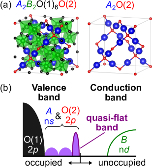
78.20.-e, 78.40.-q, 81.15.-zPyrochlore oxides are one of the typical complex oxides generally formulated as O7 and are known to exhibit a wide range of physical properties [1] such as ferro-electricity [2], superconductivity [3; 4], and frustrated magnetism [5; 6]. This crystal structure can be also denoted by O(1)6O(2) when distinctive two oxygen sites are explicitly formulated. O(1) sites form O(1)6 octahedra and O(2) sites configurate O(2) tetrahedral network as shown in Fig. 1(a). Recent theoretical studies predict that this O(2) tetrahedral network plays a crucial role in the emergence of “quasi-flat band” structure in particular pyrochlore oxides O7 (A = Sn, Pb; B = Nb, Ta) [7; 8; 9; 10]. Different from ordinary O7, where A-site element does not contribute to the band structure near Fermi level, these compounds have hybridization of filled Sn-5s (or Pb-6s) and O-2p orbitals forming the valence band maximum (VBM) as shown in Fig. 1(b). This VBM is not completely flat but flat enough in the sense that the bandwidth is much narrower than the energy scale of the band gap, which is the reason why it is called quasi-flat band. On the other hand, conduction band minimum (CBM) consists of empty Nb-4d (or Ta-5d) orbital and is far from the Fermi level. Because of this unique band structure, this class of compounds is expected to be an ideal platform for realizing numbers of emergent physical properties related with flat band structure, such as ferro-magnetism, high-temperature superconductivity, the fractional quantum Hall effect [11], and topological states [12; 13; 10].
According to the theoretical band calculations, band structure near Fermi level largely depends on the combination of A- and B-site elements [7; 8; 9; 10]. We have already reported an optical band gap of Sn2Nb2O7 epitaxial thin films and its modulation by Ti-doping in an attempt to dope holes in the quasi flat band [14]. It has been revealed that the hybridized Sn-5s and O-2p orbitals do contribute to the band structure near Fermi level, which is consistent with the theoretical predictions. In this aspect, it is gripping to examine the optical properties of other candidate materials that possibly host the quasi-flat band structures. Also, from the materials point of view, it is important to establish the growth conditions for oxides containing highly volatile elements such as tin and lead. Here, in addition to Sn2Nb2O7, we report epitaxial thin film growth of Sn2Ta2O7, Pb2Nb2O7, and Pb2Ta2O7, and their optical properties.
Epitaxial O7 (A = Sn, Pb; B = Nb, Ta) thin films were prepared on Y-stabilized ZrO2 (YSZ) (111) substrates by a pulsed laser deposition. Before the film growth, YSZ substrates were annealed in air with an electronic furnace at 1,350 for 3 hours to obtain a clear step-terrace structure with single-unit-cell height (3 Å). The targets were prepared by a hot press method in 400 Torr Ar atmosphere under a mechanical pressure of 80 MPa, starting from a mixture of SnO2, PbO, Nb2O5, and Ta2O5 powders. Chemical composition of the mixed powder for Sn2O7 targets was Sn:B = 1:1, while that for Pb2O7 was Pb:B = 1.1:1. The sintering temperature was 1,100 for Sn2O7 and 850 for Pb2O7. The films were deposited at various growth temperatures and O2 pressures by KrF excimer laser (= 248 nm) pulses at a frequency of 5 Hz. Structural properties of the films were characterized by x-ray diffraction (XRD) (Smart Lab, Rigaku) at room temperature. Chemical compositions of the films were examined by energy dispersive X-ray spectroscopy with scanning electron microscope (SEM-EDX), for which the electron beam was aligned normal to the film surface. Optical properties were measured by UV-3600 (SHIMADZU) at room temperature.
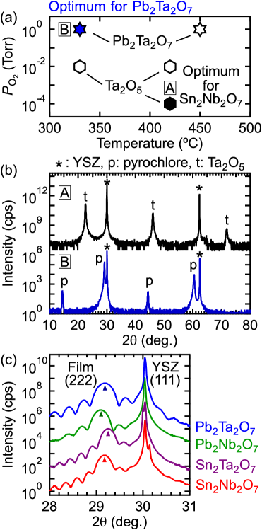
We first discuss the optimization of the thin film growth conditions. Following the growth conditions for Sn2Nb2O7 reported previously [14], we are able to obtain high-quality Sn2Ta2O7 films at the growth temperature of 420 under 10-4 Torr O2. These conditions are denoted as A in Fig. 2(a). However, in the case of Pb2Ta2O7 films, only hexagonal Ta2O5 phase appears under the same conditions (top panel of Fig. 2(b)). The same (absence of A-site element and appearance of hexagonal O5 binary oxide) has occurred for Sn2Nb2O7 as well, when the growth temperature is higher as a result of the high volatility of SnO [14]. Considering that the vapor pressure of PbO is higher than that of SnO [15], we can expect that lower growth temperature and higher O2 pressure are required to suppress the re-evaporation of PbO. Indeed, pure Pb2Ta2O7 phase appears at growth temperatures of 330 and 450 under 1 Torr O2 (Fig. 2(a)). Especially at 330, higher quality Pb2Ta2O7 film is obtained as shown in the bottom panel of Fig. 2(b). These conditions are denoted as B in Fig. 2(a), and high-quality Pb2Nb2O7 film is also obtained at this point. Here, it is worth noting that in order to compensate the short mean-free-path of the precursors under high O2 pressure ( mm at 1 Torr), the distance between the target and substrate is set as narrow as 15 mm in the fabrication of Pb2O7 and laser fluence is 2.2 J/cm2, while they are 25 mm and 1 J/cm2, respectively, for Sn2O7.
Figure 2(c) shows XRD - scan around (222) peak of Sn2Nb2O7, Sn2Ta2O7, Pb2Nb2O7, and Pb2Ta2O7 films prepared under the optimized conditions discussed above. Laue oscillations are clearly observed around the (222) main peak for all the films, indicating sharp interfaces and smooth surfaces of the films. Atomic micro scope images also show the smooth surface of the films with route-mean-square roughness of 1 nm or smaller (Fig. S2). The full width at half maximum (FWHM) of the rocking curves around (222) peaks is less than 0.07∘ for all the films (not shown), evidencing the high quality of the films as well. Reciprocal space mappings (RSM) around pyrochlore (662) peaks reveal that all the films are almost fully relaxed (Fig. S1(a)), which is expected by the rather large lattice mismatch (2–5 %) between YSZ substrate and the films as summarized in Table S1. Azimuthal () scans around pyrochlore (662) show three-fold symmetry, which is the same as that of the YSZ substrate (331), indicating that in-plane misoriented domains are indiscernible in these films (Fig. S1(b)). There has been reported a paper on reflection high energy electron diffraction (RHEED) intensity oscillation while growing thin films of a pyrochlore Tb2Ti2O7 at rather high growth temperature (750) [16]. In our case, we did not observe RHEED oscillation, presumably due to rather low growth temperatures set with considering highly volatile elements of Sn and Pb.
The chemical composition of the films is estimated by SEM-EDX. Because Nb peak is overlapped by Zr strong peak originating from YSZ substrate, the exact composition of cations in Sn2Nb2O7 and Pb2Nb2O7 films cannot be measured. However,both Sn2Ta2O7 and Pb2Ta2O7 films exhibit the stoichiometric cation ratio (Sn (or Pb)/Ta 1) within the accuracy of our measurements () in this study. Therefore, we can fairly postulate that cation off-stoichiometry is negligible in our films. Besides the cation ratio, anti-site defects Sn2+/Sn4+ (or Pb2+/Pb4+), and oxygen vacancies are also important in terms of the electronic structures of pyrochlore oxides and are indeed discussed in several previous works with bulk samples especially for Sn2Nb2O7 [17; 18; 19; 20]. However, quantitative evaluation of those is quite challenging in thin-film samples, and thus would be left for future research.
We now argue the optical properties of the films to characterize the band structures in this class of compounds. Absorption coefficient () values were calculated as below:
| (1) |
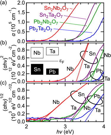
where is the film thickness, is the fraction of incident light transmitted through the film, and is the fraction of incident light reflected by the film. The absorption spectra of the films are presented in Fig. 3(a). We have already confirmed that an absorption edge of YSZ substrate locates at 4.8 eV [14] which is far away from the displayed range. The onset of sharp increase in is ranging from 2.6 to 3.4 eV. The lowest absorption-edge energy is observed in Sn2Nb2O7, followed in order by Sn2Ta2O7, Pb2Nb2O7, and Pb2Ta2O7. As we have already reported in the previous work [14], these absorption edges are plausibly assignable to a transition from the hybridized A-ns and O-2p valence band to B-nd conduction band. It is worth mentioning that precise optical measurements for thin-film samples enable us to capture the aforementioned trends, while systematic variation of band gap has been reported through reflectance measurements for bulk Sn2(Nb1-xTax)2O7 samples [18]. These results of our films confirm that the hybridized band is the common feature in this class of compounds as predicted by the first-principles band calculations [7; 8; 9; 10].
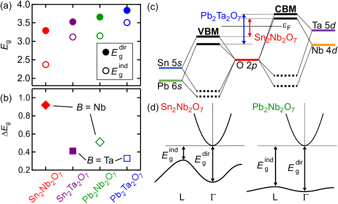
We then focus on the optical band gap () determined from the Tauc plots with considering direct and indirect allowed transitions. In Figs. 3(b) and 3(c), and are plotted as a function of , where direct and indirect band gaps ( and ) can be deduced from the intercept of the dashed line with the horizontal axis. Figure 4(a) summarizes the deduced and of all the films. As in the case of absorption edge, the narrowest band gap, both direct and indirect, is observed in Sn2Nb2O7, followed in order by Sn2Ta2O7, Pb2Nb2O7, and Pb2Ta2O7. In accordance with the observed order of the band gaps, a schematic energy level diagram of each cation around Fermi level () is illustrated in the inset of Fig. 3(b).
This tendency can be further understood by considering the energy levels of atomic orbitals for Sn-5s, Pb-6s, Nb-4d, Ta-5d, and O-2p as shown in Fig. 4(c). This diagram is based on the following consideration: (i) in this class of compounds, band gap is the energy difference between two anti-bonding orbitals; one is A-n and O-2p, and the other is B-n and O-2p, the former of which forms VBM and the latter does CBM, respectively, (ii) energy levels of the orbitals of the constituent elements are in the order of Pb-6s, Sn-5s, O-2p, Nb-4d, and Ta-5d from deeper to shallower energy. The order that Pb-6s is deeper than Sn-5s might seem unnatural because elements with the larger principal quantum number usually have shallower energy levels if their orbital angular momentum is the same, as in the case of the relationship between Nb-4d, and Ta-5d orbitals. However, this seemingly unnatural “inversion” has been actually observed in PbxSn1-xO by the fact that its band gap becomes larger by increasing the Pb doping ratio x, which is also supported by a DFT calculation [21]. This phenomenon is explained by both orbital penetration close to nucleus and relativistic effects originating from Pb-6s atomic orbital [21], and thus this can be the case for pyrochlore oxides in this study as well.
Another intriguing observation is the difference between direct and indirect band gaps () summarized in Fig. 4(b). Here, we can see two general trends: (i) when B-site is common, becomes smaller in A = Pb compounds than in A = Sn ones, (ii) when A-site is common, becomes smaller in B = Ta compounds than in B = Nb ones. According to the previously reported theoretical calculations for this class of compounds [7; 9; 10], it is revealed that VBM (CBM) becomes flattened when Sn- (Nb-)site is substituted by Pb (Ta). Especially in Nb2O7, it is clear that the direct and indirect transitions correspond to those from to points and from to points, respectively [7; 9], as schematically illustrated in Fig. 4(d). Due to this, can be a good indicator of the “flatness” in valence band; smaller indicates a flatter band with a smaller dispersion in VBM. On the other hand, for Ta2O7, CBM is also expected to be flattened and the energy levels of and points in CBM become closer [10], which makes the simple interpretation of in Nb2O7 no longer valid. Because of this more complicated CBM structure, it is not straightforward to relate the reduction in with the reduction of the band dispersion in VBM, which might be also the reason why is larger in Pb2Nb2O7 than in Sn2Ta2O7. Nonetheless, considering that VBM should reflect the nature of the A-site element as mentioned above, we speculate that Pb2Ta2O7 has a less dispersive VBM than Sn2Ta2O7. Together with the energy level diagram in Fig. 4(c), we conclude that Pb substitution in Sn2O7 has the following two effects on the band structure: (i) enlarges the band gap, (ii) reduces the band dispersion in VBM.
In summary, epitaxial O7 (A = Sn, Pb; B = Nb, Ta) (111) films are grown on YSZ (111) substrates by pulsed laser deposition. Because PbO has higher vapor pressure than SnO, higher O2 pressure is required to fabricate Pb2O7 compared with the case of Sn2O7. Optical measurements reveal that the absorption edge appears at between 2.6 and 3.4 eV in our films, which is suggestive of the existence of the hybridized A-ns and O-2p band as predicted by theoretical calculations. Both direct and indirect band gaps of Sn2Nb2O7 are the smallest, followed in order by those of Sn2Ta2O7, Pb2Nb2O7, and Pb2Ta2O7. This tendency can be interpreted by taking into account the energy levels of Sn-5s, Pb-6s, Nb-4d, and Ta-5d atomic orbitals. By comparing the difference between direct and indirect band gaps, it is clarified that Pb2O7 tends to have smaller valence band dispersion compared with Sn2O7. These general trends will be helpful for band engineering to materialize numbers of emergent phenomena expected in this class of compounds. In this regard, precise stoichiometry control should be required, which remains as future work.
This work was supported by the Japan Science and Technology Agency Core Research for Evolutional Science and Technology (JST CREST) (Grant No. JPMJCR16F1), by JSPS Grant-in-Aid for Early-Career Scientists No. JP20K15168, and by The Murata Science Foundation.
The data that support the findings of this study are available from the corresponding author upon reasonable request.
References
- Subramanian, Aravamudan, and Subba Rao [1983] M. Subramanian, G. Aravamudan, and G. Subba Rao, Prog. Solid. State Ch. 15, 55 (1983).
- Jona, Shirane, and Pepinsky [1955] F. Jona, G. Shirane, and R. Pepinsky, Phys. Rev. 98, 903 (1955).
- Hanawa et al. [2001] M. Hanawa, Y. Muraoka, T. Tayama, T. Sakakibara, J. Yamaura, and Z. Hiroi, Phys. Rev. Lett. 87, 187001 (2001).
- Sakai et al. [2001] H. Sakai, K. Yoshimura, H. Ohno, H. Kato, S. Kambe, R. E. Walstedt, T. D. Matsuda, Y. Haga, and Y. Onuki, J. Phys. Condens. Matter 13, L785 (2001).
- Ramirez et al. [1999] A. P. Ramirez, A. Hayashi, R. J. Cava, R. Siddharthan, and B. S. Shastry, Nature 399, 333 (1999).
- Gardner, Gingras, and Greedan [2010] J. S. Gardner, M. J. P. Gingras, and J. E. Greedan, Rev. Mod. Phys. 82, 53 (2010).
- Hase et al. [2018] I. Hase, T. Yanagisawa, Y. Aiura, and K. Kawashima, Phys. Rev. Lett. 120, 196401 (2018).
- Hase, Yanagisawa, and Kawashima [2018] I. Hase, T. Yanagisawa, and K. Kawashima, Nanoscale Res. Lett. 13, 63 (2018).
- Hase, Yanagisawa, and Kawashima [2019] I. Hase, T. Yanagisawa, and K. Kawashima, Nanomaterials 9, 876 (2019).
- Hase and Yanagisawa [2020] I. Hase and T. Yanagisawa, Symmetry 12, 1076 (2020).
- Liu, Liu, and Wu [2014] Z. Liu, F. Liu, and Y. S. Wu, Chinese Physics B 23, 077308 (2014).
- Zhang et al. [2019] W. Zhang, K. Luo, Z. Chen, Z. Zhu, R. Yu, C. Fang, and H. Weng, npj Computational Materials 5, 105 (2019).
- Zhou et al. [2019] Y. Zhou, K.-H. Jin, H. Huang, Z. Wang, and F. Liu, Phys. Rev. B 99, 201105 (2019).
- Ito, Fujita, and Kawasaki [2021] H. Ito, T. C. Fujita, and M. Kawasaki, APL Materials 9, 101116 (2021).
- Lamoreaux, Hildenbrand, and Brewer [1987] R. H. Lamoreaux, D. L. Hildenbrand, and L. Brewer, Journal of Physical and Chemical Reference Data 16, 419 (1987).
- Bovo et al. [2017] L. Bovo, C. M. Rouleau, D. Prabhakaran, and S. T. Bramwell, Nanotechnology 28, 055708 (2017).
- Aiura et al. [2017] Y. Aiura, K. Ozawa, I. Hase, K. Bando, H. Haga, H. Kawanaka, A. Samizo, N. Kikuchi, and K. Mase, J. Phys. Chem. C 121, 9480 (2017).
- Kikuchi et al. [2017] N. Kikuchi, A. Samizo, S. Ikeda, Y. Aiura, K. Mibu, and K. Nishio, Phys. Rev. Mater. 1, 021601 (2017).
- Samizo, Kikuchi, and Nishio [2019] A. Samizo, N. Kikuchi, and K. Nishio, MRS adv. 4, 27 (2019).
- Samizo et al. [2021] A. Samizo, M. Minohara, N. Kikuchi, K. K. Bando, Y. Aiura, K. Mibu, and K. Nishio, The Journal of Physical Chemistry C 125, 17117 (2021).
- Liao et al. [2015] M. Liao, Z. Xiao, F.-Y. Ran, H. Kumomi, T. Kamiya, and H. Hosono, ECS Journal of Solid State Science and Technology 4, Q26 (2015).
- Momma and Izumi [2011] K. Momma and F. Izumi, Journal of Applied Crystallography 44, 1272 (2011).
FIGURES


