Supporting Information
Band Versus Polaron: Charge Transport in Antimony Chalcogenides
Thomas Young Centre and Department of Chemistry, University College London, 20 Gordon Street, London WC1H 0AJ, UK
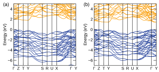
S1. Electronic band structures
S2. Fröhlich polaron coupling constant and Schultz polaron radius
| Material | ∞ | 0 | m∗ | |||
| e | h | |||||
| \ceSb2S3 | avg | 10.26 | 68.76 | 3.49 | 0.40 | 0.64 |
| x | 0.16 | 0.47 | ||||
| y | 0.92 | 0.65 | ||||
| z | 5 | 0.97 | ||||
| \ceSb2Se3 | avg | 13.52 | 76.27 | 2.57 | 0.35 | 0.90 |
| x | 0.14 | 0.85 | ||||
| y | 0.81 | 0.55 | ||||
| z | 7 | 3 | ||||
The long-range electron-longitudinal optical phonon coupling can be expressed by the dimensionless Fröhlich polaron coupling constant 1
| (1) |
where ∞ and 0 are the high-frequency and static dielectric constants, respectively, m∗ is the effective mass and is the effective phonon frequency. The effective mass and effective frequency were calculated using the AMSET package2.
The isotropic was obtained using the harmonic mean of the effective masses and the arithmetic average of the dielectric constants. The anisotropic was calculated using the anisotropic (direction-dependent) effective masses, consistent with previous work3.
| Material | v | w | m | ||||||
| e- | h+ | e- | h+ | e- | h+ | e- | h+ | ||
| \ceSb2S3 | avg | 1.6 | 2.0 | 12.70 | 12.98 | 11.16 | 10.99 | 0.52 | 0.89 |
| x | 1.0 | 1.8 | 12.34 | 12.79 | 11.39 | 11.11 | 0.19 | 0.62 | |
| y | 2.4 | 2.1 | 13.25 | 12.99 | 10.82 | 10.98 | 1.38 | 0.91 | |
| z | 5.7 | 2.5 | 16.07 | 13.30 | 9.32 | 10.79 | 14.88 | 1.47 | |
| \ceSb2Se3 | avg | 1.3 | 2.1 | 16.72 | 17.29 | 15.32 | 14.96 | 0.42 | 1.20 |
| x | 0.8 | 2.0 | 16.40 | 17.24 | 15.53 | 14.99 | 0.16 | 1.12 | |
| y | 2.0 | 1.6 | 17.21 | 16.95 | 15.01 | 15.17 | 1.06 | 0.69 | |
| z | 5.8 | 3.8 | 20.68 | 18.68 | 13.05 | 14.12 | 17.59 | 5.25 | |
Schultz polaron radius is defined as4
| (2) |
| (3) |
where v and w are Feynman-model variational parameters which specify the polaron state. They are solved variationally by the Feyman polaron model using Fröhlich polaron coupling constant as an input. is the reduced effective mass.
S3. Effect of grain boundary scattering
| Material | Calculated mobility () | ||||
| Mean free path (nm) | |||||
| - | 100 | 10 | |||
| \ceSb2S3 | x | 44.72 | 43.98 | 38.57 | |
| y | 7.13 | 7.07 | 6.55 | ||
| z | 1.35 | 1.34 | 1.25 | ||
| avg | 17.73 | 17.46 | 15.45 | ||
| ar | 33.13 | 32.82 | 30.86 | ||
| x | 15.90 | 15.77 | 14.71 | ||
| y | 11.33 | 11.25 | 10.58 | ||
| z | 8.35 | 8.29 | 7.82 | ||
| avg | 11.86 | 11.77 | 11.04 | ||
| ar | 1.90 | 1.90 | 1.88 | ||
| \ceSb2Se3 | x | 76.38 | 74.56 | 62.14 | |
| y | 11.65 | 11.46 | 10.07 | ||
| z | 1.41 | 1.39 | 1.23 | ||
| avg | 29.81 | 29.13 | 24.48 | ||
| ar | 54.17 | 53.64 | 50.52 | ||
| x | 8.38 | 8.29 | 7.57 | ||
| y | 14.63 | 14.41 | 12.78 | ||
| z | 1.95 | 1.93 | 1.81 | ||
| avg | 8.32 | 8.21 | 7.38 | ||
| ar | 7.50 | 7.47 | 7.06 | ||
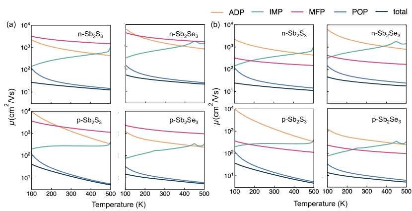
The effect of grain boundary scattering on the mobility in \ceSb2X3 was evaluated by incorporating an average grain size using the AMSET package2. The grain boundary scattering lifetime is set to , where is the group velocity and L is the mean free path. In this work, the mean free path of nd were tested. The carrier concentration and defect concentration were assumed to be and , respectively.
According to our results (Table 3 and Fig. 2), at temperatures between 100 and , the total mobility is not limited by the grain boundary scattering. The anisotropic values at room temperature are shown in Table 3. After considering the grain boundary scattering, the values of anisotropy ratio change slightly and the most favourable directions for carrier transport remain the same for both \ceSb2S3 and \ceSb2Se3.
S4. Workflow of localising a polaron in \ceSb2X3
We attempted to localise an electron or a hole in \ceSb2S3 and \ceSb2Se3 by the bond distortion method and electron attractor method (Fig. 3). A 311 supercell (with the dimension of 11.4011.20 and 11.8511.55 for \ceSb2S3 and \ceSb2Se3, respectively) was constructed, which is sufficient to model small polarons5, 6, 7. In each system, one electron per supercell was added or removed to introduce an electron or a hole.
We first applied the bond distortion method to introduce distortions around one designated atom (Sb for adding an electron and S/Se for adding a hole) for each non-equivalent Sb and S/Se. These are implemented by the ShakeNBreak package8, 9. Different distortions of 20%, 30% and 40% with both compression and stretching were considered. However, after structural optimisation, all lowest-energy structures relaxed to perfect configurations.
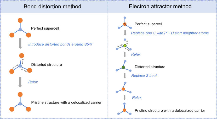
We further combined the bond distortion method with the electron attractor method to confirm the formation of hole polarons in \ceSb2S3. The electron attractor method refers to attracting electrons or holes to a particular atomic site by replacing one certain atom. Phosphorous has stronger attraction to holes than sulfur as it contains fewer protons and has a lower electronegativity. Here, we used one P to replace one S in a supercell, introduced some local distortions around the P atom and add small random displacements to all atoms to break the symmetry in the initial structures. Three non-equivalent S sites were considered, and a range of distortions of both compression and stretching between 0% and 60% with 10% as an interval were tested. The number of electrons were kept the same as the neutral replaced system, suggesting one extra hole in \ceSb2S3. The structures with the substituted atom and local distortions were fully relaxed. Finally, for each non-equivalent S case, we used the lowest-energy structures among different distortions, replaced back the S atom and relaxed the configuration again. Nevertheless, all structures went back to perfect configurations, indicating that the localised polarons are unlikely to form.
Nevertheless, we note that using a k-point mesh of 111 to do geometry relaxation could lead to localised solution in some cases (Fig. 4a). While after converging it with denser k-point mesh of 222, we finally get delocalised polarons (Fig. 4b).
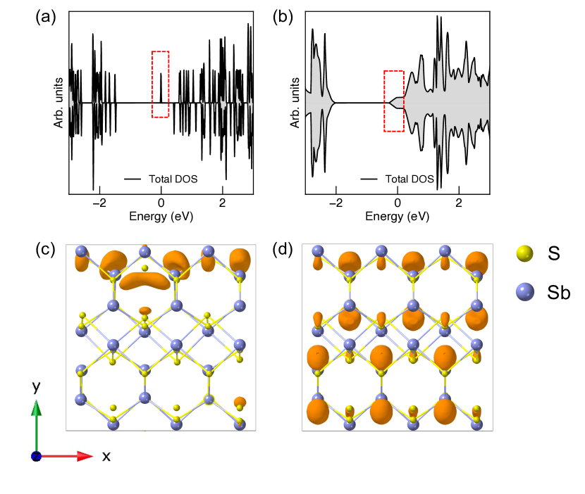
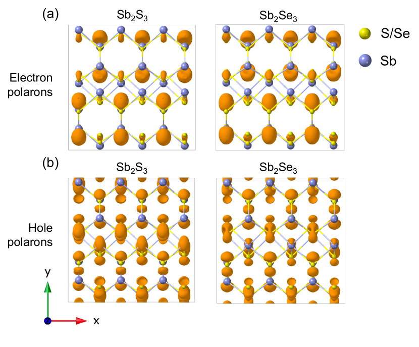
S5. Partial charge densities of electron and hole polarons
Partial charge densities of the valence band maximum (VBM) for hole polarons and conduction band maximum (CBM) for electron polarons in \ceSb2X3 are shown in Fig. 5, which are delocalised in all cases.
S6. Parameters used to calculate mobilities in \ceSb2X3
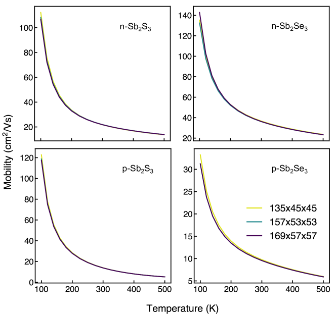
The k-point meshes used to calculate transport properties were tested (shown in Fig. 6) and a k-point mesh of 1695757 is used for all calculations. The carrier concentration was set to according to previous experimental results in \ceSb2X3 10, 11, 12, 13, 14, 15, 16. The calculated effective phonon frequency is 3.49 for \ceSb2S3 and 2.57 for \ceSb2Se3. The calculated deformation potentials, elastic constants and dielectric constants are shown in Table 4, 5 and 6, respectively.
| Material | DXX | DYY | DZZ | ||
| \ceSb2S3 | VBM | DXX | 5.41 | 0.26 | 0.07 |
| DYY | 0.26 | 0.10 | 0.02 | ||
| DZZ | 0.07 | 0.02 | 1.27 | ||
| CBM | DXX | 5.26 | 0.42 | 0.17 | |
| DYY | 0.42 | 2.43 | 3.35 | ||
| DZZ | 0.17 | 3.35 | 2.62 | ||
| \ceSb2Se3 | VBM | DXX | 0.53 | 0.16 | 0.05 |
| DYY | 0.16 | 2.86 | 0.03 | ||
| DZZ | 0.05 | 0.03 | 2.47 | ||
| CBM | DXX | 3.31 | 0.36 | 0.09 | |
| DYY | 0.36 | 0.39 | 0.29 | ||
| DZZ | 0.09 | 0.29 | 1.38 | ||
| Material | CXX | CYY | CZZ | CXY | CYZ | CZX | |
| \ceSb2S3 | CXX | 93.75 | 28.00 | 18.50 | 0.00 | 0.00 | 0.00 |
| CYY | 28.00 | 57.25 | 15.39 | 0.00 | 0.00 | 0.00 | |
| CZZ | 18.50 | 15.39 | 37.69 | 0.00 | 0.00 | 0.00 | |
| CXY | 0.00 | 0.00 | 0.00 | 31.68 | 0.00 | 0.00 | |
| CYZ | 0.00 | 0.00 | 0.00 | 0.00 | 17.11 | 0.00 | |
| CZX | 0.00 | 0.00 | 0.00 | 0.00 | 0.00 | 8.77 | |
| \ceSb2Se3 | CXX | 77.15 | 25.63 | 17.11 | 0.00 | 0.00 | 0.00 |
| CYY | 25.63 | 54.15 | 17.03 | 0.00 | 0.00 | 0.00 | |
| CZZ | 17.11 | 17.03 | 31.75 | 0.00 | 0.00 | 0.00 | |
| CXY | 0.00 | 0.00 | 0.00 | 23.42 | 0.00 | 0.00 | |
| CYZ | 0.00 | 0.00 | 0.00 | 0.00 | 18.41 | 0.00 | |
| CZX | 0.00 | 0.00 | 0.00 | 0.00 | 0.00 | 5.08 |
| Material | 0 | ∞ | ||||
| x | y | z | x | y | z | |
| Sb2S3 | 98.94 | 94.21 | 13.14 | 11.55 | 10.97 | 8.25 |
| Sb2Se3 | 85.64 | 128.18 | 15.00 | 15.11 | 14.92 | 10.53 |
References
- Fröhlich 1952 Fröhlich, H. Interaction of electrons with lattice vibrations. Proc. Math. Phys. Eng. 1952, 215, 291–298
- Ganose et al. 2021 Ganose, A. M.; Park, J.; Faghaninia, A.; Woods-Robinson, R.; Persson, K. A.; Jain, A. Efficient calculation of carrier scattering rates from first principles. Nat. Commun. 2021, 12, 1–9
- Guster et al. 2021 Guster, B.; Melo, P.; Martin, B. A.; Brousseau-Couture, V.; de Abreu, J. C.; Miglio, A.; Giantomassi, M.; Côté, M.; Frost, J. M.; Verstraete, M. J., et al. Fröhlich polaron effective mass and localization length in cubic materials: degenerate and anisotropic electronic bands. Phys. Rev. B 2021, 104, 235123
- Schultz 1959 Schultz, T. Slow electrons in polar crystals: self-energy, mass, and mobility. Phys. Rev. 1959, 116, 526
- Sun et al. 2017 Sun, L.; Huang, X.; Wang, L.; Janotti, A. Disentangling the role of small polarons and oxygen vacancies in \ceCeO2. Phys. Rev. B 2017, 95, 245101
- Ding et al. 2014 Ding, H.; Lin, H.; Sadigh, B.; Zhou, F.; Ozolins, V.; Asta, M. Computational investigation of electron small polarons in -\ceMoO3. J. Phys. Chem. C 2014, 118, 15565–15572
- Castleton et al. 2019 Castleton, C. W.; Lee, A.; Kullgren, J. Benchmarking density functional theory functionals for polarons in oxides: Properties of \ceCeO2. J. Phys. Chem. C 2019, 123, 5164–5175
- Mosquera-Lois and Kavanagh 2021 Mosquera-Lois, I.; Kavanagh, S. R. In search of hidden defects. Matter 2021, 4, 2602–2605
- Mosquera-Lois et al. 2022 Mosquera-Lois, I.; Kavanagh, S. R.; Walsh, A.; Scanlon, D. O. Identifying the ground state structures of point defects in solids. arXiv preprint arXiv:2207.09862 2022, (accessed on 25/07/2022)
- Chen et al. 2017 Chen, C.; Bobela, D. C.; Yang, Y.; Lu, S.; Zeng, K.; Ge, C.; Yang, B.; Gao, L.; Zhao, Y.; Beard, M. C., et al. Characterization of basic physical properties of \ceSb2Se3 and its relevance for photovoltaics. Front. Optoelectron. 2017, 10, 18–30
- Liu et al. 2016 Liu, M.; Gong, Y.; Li, Z.; Dou, M.; Wang, F. A green and facile hydrothermal approach for the synthesis of high-quality semi-conducting \ceSb2S3 thin films. Appl. Surf. Sci. 2016, 387, 790–795
- Zhou et al. 2014 Zhou, Y.; Leng, M.; Xia, Z.; Zhong, J.; Song, H.; Liu, X.; Yang, B.; Zhang, J.; Chen, J.; Zhou, K., et al. Solution-processed antimony selenide heterojunction solar cells. Adv. Energy Mater. 2014, 4, 1301846
- Yuan et al. 2016 Yuan, C.; Zhang, L.; Liu, W.; Zhu, C. Rapid thermal process to fabricate \ceSb2Se3 thin film for solar cell application. Sol. Energy 2016, 137, 256–260
- Li et al. 2021 Li, J.; Huang, J.; Li, K.; Zeng, Y.; Zhang, Y.; Sun, K.; Yan, C.; Xue, C.; Chen, C.; Chen, T., et al. Defect-resolved effective majority carrier mobility in highly anisotropic antimony chalcogenide thin-film solar cells. Sol. RRL 2021, 5, 2000693
- Chalapathi et al. 2020 Chalapathi, U.; Poornaprakash, B.; Park, S.-H. Influence of post-deposition annealing temperature on the growth of chemically deposited \ceSb2S3 thin films. Superlattices Microstruct. 2020, 141, 106500
- Black et al. 1957 Black, J.; Conwell, E.; Seigle, L.; Spencer, C. Electrical and optical properties of some MN semiconductors. J. Phys. Chem. Solids 1957, 2, 240–251