Electronic structure of Humble defects in Ge and Ge0.8Si0.2
Abstract
The group-IV diamond-structure elements are known to host a variety of planar defects, including {001} planar defects in C and {001}, {111} and {113} planar defects in Si and Ge. Among the {001} planar defects, the Humble defect, known for some time to occur in Ge, has recently also been observed in Si/Ge alloys, but the details of its electronic structure remain poorly understood. Here we perform first-principles density functional calculations to study Humble defects in both Ge and Ge0.8Si0.2. We also measure the Si L2,3-edge electron energy loss spectra both at the defect and in a bulk-like region far from the defect, and compare with theoretical calculations on corresponding Si sites in our first-principles calculations. We find that inclusion of core-hole effects in the theory is essential for reproducing the observed L2,3 edge spectra, and that once they are included, the results provide a set of fingerprints for different types of local atomic bonding environments in Ge0.8Si0.2. Our first-principles calculations reveal that the Humble defects have a tendency to enlarge the electronic band gap, which may have potential uses in band engineering. The use of hybrid functionals for an improved description of the band gap in these systems is also discussed.
I Introduction
Group IV elements, especially Si and Ge, are now widely used in semiconductor devices Paul (2004), optoelectronics Fadaly et al. (2020), and recently developed quantum information and computing technologies Scappucci et al. (2020). Generally, defects in these materials affect the device properties, with some even exhibiting useful properties that could be utilized for practical applications Queisser and Haller (1998). Consequently, the properties of these defects are of considerable interest for both theoretical and experimental studies.
One important type of defect is the extended planar defect. A well-known example is the {001} planar defect in natural diamond Lang (1964); Humble and Hirsch (1982); Olivier et al. (2018), where recent experimental work has shown that defect pairs have a zigzag order Olivier et al. (2018). In Si, the {111} Jeng et al. (1988); Muto et al. (1991); Akatsu et al. (2005) and {113} Takeda (1991); Dudeck et al. (2013) planar defects are the most common ones. {001} planar defects have also been reported in Si and Ge after hydrogen implantation Akatsu et al. (2005). In Ge, {001} Muto and Takeda (1995); David et al. (2007), {111} David et al. (2007), and {113} Lima and Howie (1976); David et al. (2007); Akatsu et al. (2005) defects have been reported. However, only a few of them have been examined using atomic-resolution high-angle annular dark-field (HAADF) imaging Dudeck et al. (2013); Olivier et al. (2018), making it difficult to distinguish between proposed atomic structures. Alternatively, one can use electron energy-loss spectroscopy (EELS) to extract quantitative information regarding the local atomic bonding and chemical environments in the vicinity of the defect, but this has been done only for a few planar defects, e.g., for the {001} planar defect in diamond Olivier et al. (2018).
Several structural models have been proposed to describe the atomic structure of {001} planar defects. In 1964, Lang proposed the first model which assumes that these defects in diamond consist of nitrogen platelets Lang (1964). However, the role of three-fold coordinated nitrogen in the {001} planar defects of diamond is still controversial. Later, in 1982, Humble proposed another model in which the planar defects in diamond consist entirely of four-coordinated carbon atoms Humble and Hirsch (1982). Goss et al. elaborated the Humble model into five distinct sub-models corresponding to different arrangements of the atoms residing in the defect layer, denoted as Humble models (a) to (e) Goss et al. (2001, 2002, 2003). Even though the Humble model was initially proposed for {001} planar defects in diamond, later work has not confirmed its existence in diamond, or for that matter, in Si. Instead, the Humble defect was observed first in Ge Muto and Takeda (1995) and much more recently in a Ge0.8Si0.2 alloy Yang et al. (2021).
Planar defects in semiconductors have been the subject of a variety of computational approaches. Studies on planar defects in Si have been carried out using molecular dynamics simulations Kapur and Sinno (2010); Dudeck et al. (2013), empirical potentials and tight-binding models Arai et al. (1997), and density-functional theory (DFT) calculations Goss et al. (2002). Also, Goss et al. employed DFT to study planar defects in diamond Goss et al. (2001, 2003). Although the Humble defects have been experimentally observed in Ge Muto and Takeda (1995) and a Ge0.8Si0.2 alloy Yang et al. (2021), we are not aware of any theoretical studies focusing on the electronic properties of Humble defects in these materials.
In this work, we use first-principles DFT calculations to investigate the electronic properties of Humble defects in Ge and Ge0.8Si0.2, which we denote as GeSi henceforth. We also carry out experimental measurements of the Si L2,3-edge EEL spectra in the defects and in nearby bulk regions of GeSi at room temperature, and compare our theoretical spectra with experiments. Our calculations reveal that core-hole effects play an important role in describing the Si L2,3-edge EEL spectra of the Humble defects in GeSi. We also find that the electronic band gap is locally enhanced in the vicinity of the Humble defects, potentially offering a unique platform for band engineering. The use of hybrid functionals to obtain an improved description of the band gaps in these systems is also discussed.
This paper is organized as follows: In Sec. II we briefly introduce the Lang and Humble models. In Sec. III we provide details of our DFT calculations (Sec. III.1) and EELS measurements (Sec. III.2). We present the electronic properties of bulk Ge and GeSe in Sec. IV, and show how the DFT band-gap problem, which is particularly severe for bulk Ge, can be fixed by performing hybrid-functional DFT calculations. Section V provides futher discussion of the electronic properties of the Humble defects in Ge and GeSi, focusing on the effect on the local band gap. The EELS measurements and their comparison with simulations are presented in Sec. VI, both in the bulk-like region (Sec. VI.1) and the in the defect core (Sec. VI.2). We summarize our findings and conclude in Sec. VII.
II The Lang and Humble models
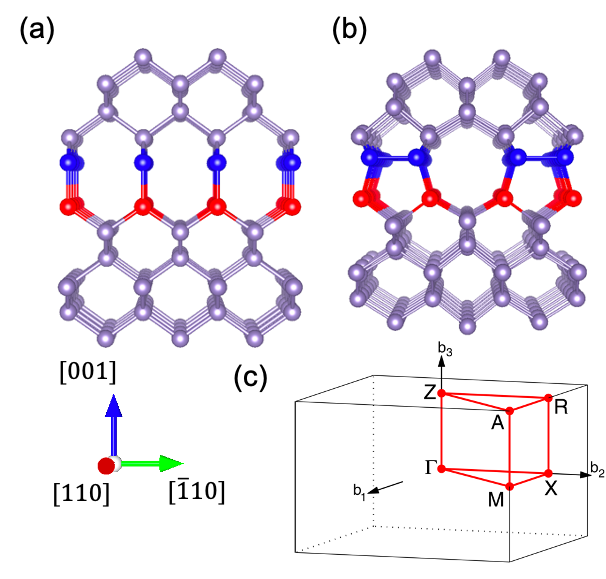
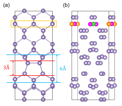
Before presenting the Humble model Humble and Hirsch (1982), it is instructive to revisit the Lang model Lang (1964), which can be regarded as the predecessor of the Humble model. Lang initially proposed this model to describe the {001} planar defect in diamond. As shown in Fig. 1(a), there are two layers of nitrogen atoms in the Lang model, shown as red and blue. The perfect diamond structure can be recovered by removing one of these two defect layers and rebonding the atoms with dangling bonds. We will use the terminology of “defect core” to denote the two layers of defect atoms in the Lang model, and in the Humble model as well. The atoms in the bulk are all four-coordinated, whereas the atoms in the defect core are three-coordinated. If the defect core consists of column-IV atoms as in the bulk, these atoms would have costly dangling bonds, an observation that motivated Lang to suggest trivalent N atoms for the core sites instead.
Unlike the Lang model, atoms in the Humble defect core are four-coordinated, just as they are in the bulk. The Humble model can be derived from the Lang model by pairing neighboring core atoms and moving them closer to one another to form a dimer bond, thereby removing two dangling bonds and converting all atoms to fourfold coordination. As shown in Fig. 1(b), the red atoms in the Humble model are displaced in the direction to form dimers, while the blue atoms are displaced in the direction, relative to the Lang model.
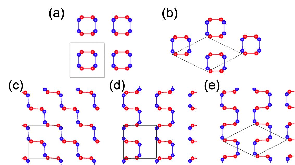
Humble’s initial proposal assumed one particular pairing arrangement in the defect core, but other atomic arrangements are possible. In Refs. Goss et al. (2001, 2002, 2003), the original Humble model was extended by proposing five different possible types of atomic arrangements in the core, denotes as types (a) to (e), as shown in Fig. 2, with the original model corresponding to model (a). These five Humble models have been studied theoretically in diamond Goss et al. (2001, 2003) and Si Goss et al. (2002).
III Methods
III.1 DFT calculations
All the reported DFT calculations are performed using the Vienna Ab-initio Simulation Package (VASP) Kresse and Furthmüller (1996) and the projector-augmented wave Blöchl (1994); Kresse and Joubert (1999) method with Ge and Si pseudopotential valence configurations. Standard DFT calculations employ the generalized-gradient-approximation (GGA) exchang-correlation functional of Perdew, Burke, and Ernzerhof (PBE) Perdew et al. (1996), henceforth denoted as GGA-PBE. The convergence criteria for forces and energies during structural relaxation are and eV respectively. In some cases, band structures and gaps are also computed using the HSE03 hybrid functional Heyd et al. (2003); Heyd and Scuseria (2004); Heyd et al. (2006). In those cases, the experimental lattice constants are used in the calculation. The cutoff energies for the plane-wave basis set are 500 and 400 eV for GGA-PBE and HSE03, respectively. Other numerical details such as the size of the k-points mesh or the inclusion of spin-orbit coupling or whether the hybrid functional is used will be specified below.
The virtual crystal approximation (VCA) as implemented in Ref. Bellaiche and Vanderbilt (2000) is used when simulating the Ge0.8Si0.2 alloy. In this approach, every atom is identical, with an identity that is a mix of 80% Ge and 20% Si in the Ge0.8Si0.2 material. The VCA takes care of averaging over the ensemble of all possible distributions in a mean-field sense. The AFLOW Setyawan and Curtarolo (2010) online tools are used to analyze the structure, and the PyProcar Herath et al. (2020) package is used for the post-processing of the electronic structure data.
III.2 Electron energy loss spectroscopy
The Si L2,3 edge EEL spectra are acquired using a scanning transmission electron microscope equipped with a electron monochromator. In our experiments, the size of our electron beam is about 2 Å, small enough to allow separate imaging of the bulk and defect regions of Ge0.8Si0.2. To avoid radiation damage, a rectangular scan window is placed at the defect or bulk region during EEL spectra acquisition. We use the monochromator to improve the energy resolution to about 100 meV and use an EELS detector dispersion of 25.7 meV/pixel. After focusing the zero-loss peak, the spectrometer is further tuned to obtain optimal focus in the vicinity of 100 eV, close to the Si L2,3 edges of interest. With a detector dwell time of 2 sec, 30 to 50 EEL spectra are taken in serial and summed to obtain good statistics. We then fit and subtract an exponential background from the spectra and perform a deconvolution to obtain the Si L3 edge spectra presented in Sec. VI.
IV Bulk properties of Ge and Ge0.8Si0.8
| Lattice constant (Å) | Band gap (eV) | |||
|---|---|---|---|---|
| GGA-PBE | Exper. | HSE03 | Exper. | |
| Ge | ||||
| Ge0.8Si0.2 | ||||
We start from bulk Ge and Ge0.8Si0.2. Due to the quasi-random distribution of atoms in the Ge0.8Si0.2 alloy, it is computationally challenging to simulate the Ge0.8Si0.2 alloy within DFT. Here we employ the virtual crystal approximation (VCA) as implemented in Ref. Bellaiche and Vanderbilt (2000) to construct a virtual atom which is a mixture of 80% Ge and 20% Si, and then build the Ge0.8Si0.2 structures consisting of the virtual atoms. Due to the similarities between the Ge and Si atoms, we expect the results obtained using the VCA to provide a reasonable description of the studied system.
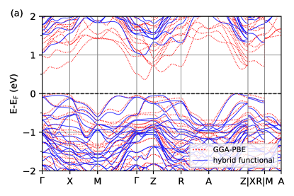
First, we use GGA-PBE to relax the bulk Ge and Ge0.8Si0.2 diamond structures. The relaxation is performed on a two-atom primitive unit cell with a Monkhorst-Pack (MP) Monkhorst and Pack (1976) k-mesh. The GGA-PBE optimized lattice constants of bulk Ge and Ge0.8Si0.2 are summarized and compared with experiment in Table 1. The GGA-PBE calculation slightly overestimates the lattice constants, but it severely underestimates the electronic band gap. The GGA-PBE predicts both the bulk Ge and Ge0.8Si0.2 systems to be semimetals, as shown in Fig. 3, although both these systems are experimentally known to be semiconductors. We therefore tested all of the local-density approximation (LDA) and GGA exchange-correlation functionals implemented in VASP, but confirmed that all of them incorrectly predict bulk Ge to be a semimetal, in agreement with previous DFT studies Igumbor et al. (2017). However, hybrid functionals Heyd et al. (2003); Heyd and Scuseria (2004); Heyd et al. (2006) are known to correctly predict a non-zero band gap in bulk Ge Deák et al. (2010). We therefore adopt the HSE03 hybrid functional Heyd et al. (2003); Heyd and Scuseria (2004); Heyd et al. (2006) for an improved description of band-structure properties in this work.
The HSE03 results for the band gaps are also presented in Table 1. These are computed at the experimental lattice constants given in the Table. Due to the computational expense of the HSE03 calculations, we use an MP k-mesh for the self-consistent part of the HSE03 calculation with a plane-wave energy cutoff of 400 eV. The HSE03 band structures are shown in Fig. 3. An indirect band gap is observed for both Ge and Ge0.8Si0.2 and the gap values are in good agreement with experiment.
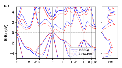
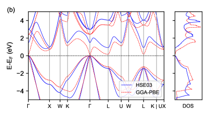
We also calculate the density of states (DOS) using both the GGA-PBE and HSE03 functionals, as shown in the right panels of Fig. 3. It is evident that the GGA-PBE DOS in the conduction-band region almost matches that of the HSE03 one except for a rigid shift of states along the energy axis. This is reasonable because the momentum-space dispersion of the conduction bands does not change substantially between the GGA-PBE and HSE03 calculations, as can be seen in Fig. 3. The HSE03 correction to the bulk Ge and Ge0.8Si0.2 band structures can thus be said to be of the “scissors” type.
We now discuss the role of Si alloying on the electronic band structure of bulk Ge. As shown in Fig. 3 and Table. 1, the HSE03 band gap is enlarged in the Ge0.8Si0.2 alloy compared to pristine Ge. Both Ge and Ge0.8Si0.2 exhibit an indirect band gap. For Ge the indirect band gap is from to , whereas for Ge0.8Si0.2 it is from to the valley near along –. This agrees well with experimental data obtained using EELS Batson and Morar (1991); Batson (1995) and another theoretical work performed using nonlocal empirical pseudopotentials Fischetti and Laux (1996). Besides the above-mentioned minor differences, the overall electronic properties of bulk Ge and Ge0.8Si0.2 are very similar.
V Humble defects in Ge and Ge0.8Si0.2
The Humble defects are experimentally observed in both Ge Muto and Takeda (1995) and Ge0.8Si0.2. The DFT calculations show that the Humble (a) defect is energetically the most favorable one among the five distinct Humble defects models shown in Fig. 2 Yang et al. (2021); for both Ge and GeSi, Humble defects (b-e) are at least 45 meV (per interstitial atom) higher in energy, as reported in Ref. Yang et al. (2021). Therefore, here we focus only on the Humble defect (a) in Ge and Ge0.8Si0.2 and calculate its electronic properties. If not specified, the word “Humble defect” henceforth denotes the Humble (a) defect.
The Humble structure is built by the procedure mentioned in Sec. II. The supercell consists of 52 atoms in 13 layers, and we assume periodic boundary conditions in all three dimensions. The space group of the Humble structure is (no. 115). The relaxation is performed using GGA-PBE with a MP grid of k-points. The in-plane lattice constants ( and ) are fixed to the bulk value obtained from the GGA-PBE relaxation of the defect-free bulk structure, whereas the supercell lattice constant is allowed to relax. The relaxed lattice constants are reported for the Ge and Ge0.8Si0.2 Humble structures in the middle column of Table. 2.
| Lattice constants (Å) | Band gap (eV) | ||
|---|---|---|---|
| Ge | |||
| Ge0.8Si0.2 | |||
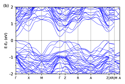
The calculated electronic band structures of the GGA-PBE optimized 13-layer Humble structures are presented in Fig. 4. The band structures of the two Humble structures are very similar, suggesting that the Ge Humble structure can be used as a good approximation for the Ge0.8Si0.2 one. Surprisingly, our GGA-PBE calculations predict both the Ge and Ge0.8Si0.2 Humble structures to be small-gap insulators, even though the same GGA-PBE calculations predict defect-free bulk Ge and Ge0.8Si0.2 to be semimetallic. That is, we find that the introduction of Humble defects in bulk Ge or Ge0.8Si0.2 tends to open the band gap. The computed gaps of the two Humble structures are listed in Table. 2. Notably, the band gap for each structure is indirect; the valence-band maximum is between the to point, whereas the conduction-band minimum is at the point of the Brillouin zone.

In Appendix A, we report the HSE03-calculated band structures of the Ge and Ge0.8Si0.2 Humble structures. However, due to the computational expense, these calculations were performed on a 9-layer Humble structures instead of the 13-layer ones used here. We again find that the HSE03 correction to the GGA-PBE band structure is of the scissors type, so that the DOS of the conduction bands calculated within the HSE03 approximation is very close to those given by GGA-PBE after a rigid shift in energy. This suggests that the DOS calculated using the GGA-PBE can be used to simulate the experimental EEL spectra, an expectation that is borne out by the good agreement between theory and experiment that is presented below.
VI EEL spectra of the Humble defect: experiments and simulations
In the past, core-loss EELS has mainly been used to differentiate between different chemical bonding environments of a given element Rez and Muller (2008). Here, we use Si L2,3-edge spectroscopy to distinguish between defected and bulk-like regions of a Ge0.8Si0.2 sample, even though all the atoms are four-fold coordinated. We work with an instrumental energy resolution of meV, noting that under these conditions the EELS spectra are still limited mainly by the core-hole lifetime Klima (1970); Altarelli and Dexter (1972). After deconvoluting to obtain the L3 edge spectra, the resolution is sufficient for a direct comparison with theory. The EEL spectra are measured in the bulk region and at the defect core. As discussed in Sec. III.2, the defect core spectra are measured separately for electron beam subscan windows with heights of and as indicated in Fig. 5(a).
In the EELS measurement, the differential cross section for electron scattering is given by Weng et al. (1989)
| (1) |
where is the Lorentz factor, is the Bohr radius, is the momentum transfer, is the electric-dipole transition matrix element slowly varying with energy, is the initial core-level state, is the final conduction state, and is the angular-momentum-resolved DOS. Here we have assumed the dipole selection rule () for the transitions from the core-level to the conduction states. For the Si L3 edges, since the is the Si core-level state, the EELS is only sensitive to final states of predominant or character.
As mentioned in Sec. V, the Humble structure in Ge and Ge0.8Si0.2 have very similar electronic structures. Considering the similarity between Si and Ge atoms and the fact that an average of 80% of the neighbors of any given Si site are Ge atoms, we now abandon the use of the VCA and work instead in the limit of low Si concentration. That is, we carry out calculations using supercells in which only a single Si atom has been substituted into the Ge Humble structure, and vary the location of this impurity atom to take statistical averages.
A further complication is that a core hole is formed when a core electron is ejected, giving rise to an interaction with the conduction bands. In most cases, such a “core-hole effect” cannot be neglected, especially in insulators Duscher et al. (2001); Rez and Muller (2008). Accordingly, we adopt the “Z+1 approximation,” in which the excitation is simulated with an extra proton in the nucleus of the excited Si atom Lee and Beni (1977); Buczko et al. (2000); Duscher et al. (2001); Rez and Muller (2008); Zhou et al. (2012). Using the structure as obtained from a relaxation without the core hole, we replace the Si atom with a P atom and then calculate the - and -projected local DOS on the P atom. Typically, a large supercell is needed to avoid interactions between periodic images of the Z+1 atoms. We have tested supercells having 52, 104, and 208 atoms, and find that good convergence is achieved for the 104-atom cell. Conversely, if the core-hole effect is negligible or fully screened, one can use the local - and -projected DOS for an ordinary Si impurity; we refer to this as the “Z approximation” Weng et al. (1989, 1990); Rez and Muller (2008).
The spin-orbit coupling is included while implementing the Z and Z+1 approximations. To save computational expense, these supercell calculations are carried out using GGA-PBE rather than HSE03. In Appendix A, we show that the correction coming from HSE03 is again mainly of the scissors type. That is, the DOS of the conduction bands calculated using GGA-PBE and HSE03 are very similar after a rigid upward shift of the GGA-PBE calculated conduction bands. As will be shown below, we find that the GGA-PBE simulations give good agreement with our experimental EELS data.
All the reported EELS simulations are performed in 13-layer Humble structures. We include enough conduction bands so that all states up to 8 eV above the valence-band maximum are included. For the calculation of the partial DOS, the considered Wigner-Seitz radii for Si and P are 1.312 and 1.233 Å, respectively. The DOS is broadened by a Gaussian function with a width of 0.05 eV.
VI.1 Bulk-like region
In this section, we present our results for the EELS measurements and simulations in the bulk-like region of the Humble structure, i.e., far from the Humble defect layer. The EEL spectrum in the bulk-region is measured 1 nm away from the defect core, and is essentially identical if measured 3 nm away. For the simulations, the most bulk-like atoms in the 13-layer Humble structure are the four atoms in the sixth atomic layer above or below the defect core, as shown in Fig. 5. We carry out two sets of calculations, one with the Si atom located at the most energetically favorable of the four sites, and the other assuming a uniformly distributed over all four sites.
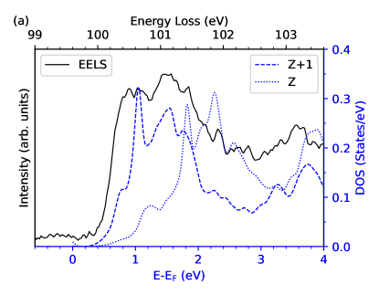
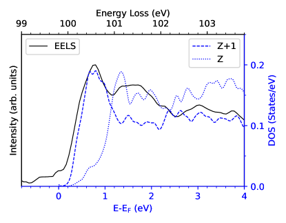
For the first case, we determine the lowest-energy site for the substitution of Si atom by computing the energy cost of the substitution at each site. By symmetry there are three inequivalent sites, denoted as the corner, edge, and center sites in Fig. 5(b), We find the corner site to be most favorable, with the edge and center sites are higher by 57 and 96 meV respectively. Then we apply both the Z and Z+1 approximation to the Si atom at this site to simulate the EEL spectrum measured in the bulk region. The experimental data are compared with the theoretical results in Fig. 6(a).
For the second case, we obtain the simulated EEL spectrum at each of the three unique sites separately, and average them as
| (2) |
with weights for corner and center sites and 0.5 for the edge sites. The resulting Z and Z+1 spectra are shown in Fig. 6(b).
From Fig. 6, it is evident that the Z+1 approximation is in very good agreement with the EEL spectrum no matter which of these two approaches we adopt. On the other hand, the Z approximation fails to predict the peaks below 2 eV, but it still provides some information about peaks above 2 eV. This indicates that the core-hole effects cannot be neglected while simulating the EELS measured in the bulk region.
In the simulations described above, we only substitute one Ge atom at a time by Si (or P) in the Humble supercell. In other words, no nearest-neighbor Si-Si bonds are considered. In Appendix B, we investigate the effect of such Si-Si bonds by substituting two Ge atoms simultaneously. The results show that Si-Si bonds do not change the excitation spectra substantially, suggesting that the single-impurity approximation is sufficient to model the behavior of Si atoms in the Ge0.8Si0.2 Humble structure.
VI.2 Defect region
In the previous subsection, we used the Z and Z+1 approximations to simulate the EEL spectrum and compared it with measurements in the bulk-like region of the sample. Here we present similar comparisons, but for the defect region.
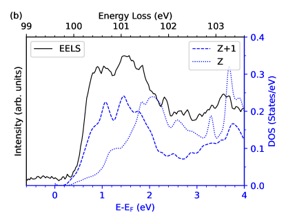
In the defect core, EEL spectra are separately measured within 3 Å and a 6 Å integration windows. Both windows are centered around the defect core, as shown in Fig. 5(a). The 3 Å window spans only the defect core, as shown by the red and blue atoms in Fig. 1(b), while the 6 Å window includes two more layers adjacent to the core. The experimental EEL spectra and the theoretical simulations, are shown in Figs. 7 and 8.
By comparing Fig. 6 with Figs. 7 and 8, it is clear that the EEL spectra measured in the bulk and defect regions are significantly different, although all Si atoms are four-fold coordinated in both regions. This suggests that some more subtle difference in local bonding configuration must be responsible. Similar differences are expected in the comparison of the spectra for the different spatial windows defined in Fig. 7 and Fig. 8, since the 6 Å window in Fig. 8 also covers some atoms outside the defect core.
In the spectrum measured within the window, the intensity of the peak below eV is relatively higher, when compared to the intensity of the adjacent peak lying in the - eV range of the same spectrum, than that of in the -window spectrum. This suggests that the highest peak below 1 eV might serve as a fingerprint of the Humble defect.
Next, we compare our experimental measurements with the theoretical simulations. From Figs. 7 and 8, we find that the Z+1 approximation works well in both cases, although the peak intensities between 1 eV to 2 eV are slightly underestimated. On the other hand, the Z approximation does not work very well near the edge onset, which indicates that the core-hole effect cannot be neglected in this system.

VII Discussion and conclusion
In summary, we first calculated the band structures of bulk Ge and Ge0.8Si0.2 at the GGA-PBE level. Although both materials are insulating experimentally, LDA and GGA calculations predict them to be semimetallic due to the well-known band gap problem of DFT. This issue was resolved by performing HSE03 hybrid-functional calculations, which correctly predict band gaps that are in good agreement with experiment.
Next, we used the GGA-PBE to calculate the electronic properties of the Ge and Ge0.8Si0.2 Humble structures. These are both insulating in our calculations, although their defect-free bulk structures are predicted to be semimetallic when calculated in the same way. This indicates that the Humble defect can locally enlarge the band gap of Ge and Ge0.8Si0.2, a fact that may potentially be useful in band engineering. We also found that the DOS calculated using HSE03 is very nearly a rigid shift of that calculated using GGA-PBE, justifying the use of the GGA-PBE calculations for the simulation of the EEL spectra.
We have separately measured the Si L3 edge EEL spectra in Ge0.8Si0.2 in a bulk-like region and at the Humble defect. To simulate the EEL spectra, we used a single Si atom in the Ge Humble structure to mimic the Si atom in the Ge0.8Si0.2 alloy, and we placed the Si atom at various sites to simulate the EEL spectra measured from different regions. We think this is a good approximation for three reasons. (i) The band-structure calculations show that the Ge and Ge0.8Si0.2 Humble structures have similar electronic properties. (ii) The chemical properties of Si are similar to those of Ge, and the concentration of Si is relatively low. (iii) The Si-Si bond was not found to have a strong effect on the simulated EEL spectra. We implemented both the Z and Z+1 approximations to simulate the EEL spectra, corresponding to the absence and presence of the core hole, respectively. The spectra simulated using the Z+1 approximation were in much better agreement with experiment, especially near the edge onset, indicating that the core-hole effect is not negligible, as might be expected given that the studied system is semiconducting so that no metallic screening of the core-hole occurs.
However, the intensities of a few peaks were still not well predicted by theory. There are several possible reasons. Firstly, the EEL spectra are measured in the Ge0.8Si0.2 alloy. Due to the randomness of the alloy, the electron momentum is no longer a good quantum number. As a result, the dipole selection rules in Eq. (1) may be changed due to the disorder. Secondly, the presence of some Si-Si bonds can affect the intensities of peaks. This effect is discussed in Appendix. B, where we find that a Si neighbor of the Si core hole has little effect on the position of the peaks but does change their intensities. Thirdly, we have assumed that and in Eq. (1) are the same. However, in Refs. Weng et al. (1989, 1990), it is reported that the ratio of the intensities of the and transitions is about 2 : 1. We tried using this ratio in the Z+1 calculation, but the ratio of 1 : 1 actually fits better with the experimental measurements. A proper determination of this ratio would require use of an all-electron method Duscher et al. (2001). Finally, both the Z and Z+1 approximations are based on a single-particle picture. A more accurate treatment of the electron-hole interaction could be carried out by solving the Bethe-Salpeter equation Shirley (1998); Benedict et al. (1998); Rohlfing and Louie (1998); this could be a possible direction for further studies, but is beyond the scope of the present work.
Acknowledgments
First-principles DFT calculations were performed using the Rutgers University Parallel Computing (RUPC) clusters. We thank Viktor Oudovenko for his technical assistance. We also thank Emily Turner and Kevin S. Jones for preparing the sample. S.R. and D.V. were supported by NSF Grant DMR-1954856. S.S. acknowledges the support from the Office of Naval Research grant N00014-21-1-2107 and the U.S. Department of Energy (DOE), Office of Science, Basic Energy Sciences under award DE-SC0020353. H.Y. and E.G. acknowledge the financial support from the US Department of Energy, under award number DE-EE0008083.
Appendix A Band structures of Humble defects in Ge and Ge0.8Si0.2: A hybrid functional study

| Lattice Constants (Å) | Band Gap | ||
|---|---|---|---|
| (eV) | |||
| Ge (GGA-PBE) | |||
| Ge (HSE03) | |||
| Ge0.8Si0.2 (GGA-PBE) | |||
| Ge0.8Si0.2 (HSE03) | |||
In this work, we have made use of two approximations. Firstly, we use the DOS calculated from GGA-PBE instead of the more accurate HSE03. Secondly, we use the Ge Humble structure to approximate the Ge0.8Si0.2 Humble structure. In this Appendix, we justify these two approximations by comparing the band structures of 9-layer Ge and Ge0.8Si0.2 Humble structures. We use both GGA-PBE and HSE03 to calculate the bands for each structure.
Figure 9 shows the band structures of the 9-layer Ge and Ge0.8Si0.2 supercells in panels (a) and (b) respectively. For each panel, the GGA-PBE bands, shown as dotted red lines, are calculated for the DFT-relaxed structure as reported in Table. 3. Although bulk Ge and Ge0.8Si0.2 are semi-metallic if calculated using the GGA-PBE, each Humble structure is insulating with an indirect band gap.
The solid blue lines in Fig. 9 show the HSE03 bands for the Ge and Ge0.8Si0.2 Humble structures respectively. To save computational cost, we use a MP grid of k-points for the self-consistent field calculations. As in Sec. IV, we use the experimental lattice constants when calculating HSE03 bands. However, because we do not have the experimental lattice constant for the Ge Humble structure, we determine it by fitting the stress to the value calculated for the bulk at the experimental lattice constant. The lattice constant for the Ge0.8Si0.2 Humble structure is measured experimentally.
By comparing panels (a) and (b) in Fig. 9, we again find that the Ge and Ge0.8Si0.2 Humble structures have similar band structures, and the momentum-space dispersion of GGA-PBE and HSE03 bands are very similar.
Appendix B The effect of Si-Si bonds in simulations of the EEL Spectra
In Appendix A, we have argued that we can use the Ge Humble structure to approximate the Ge0.8Si0.2 one. We implement this approximation when simulating EEL spectra, and we only replace one atom by Si in the Ge Humble structure. As a result, no Si-Si bond is considered in the simulation. Due to the low concentration, the Si atom tends to form bonds with Ge atoms. Therefore, the effect of Si-Si bonds should be minor. However, it is instructive to check how the Si-Si bond affects the simulation of the EEL spectra.
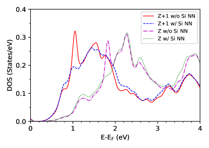
Similar to what we have done in Sec. VI, we use a 13-layer Ge Humble structure, but with two Ge atoms replaced by Si. One of these is located at the corner site in the bulk-like layer, as in Fig. 6(a), and another Si atom is its nearest neighbor. Then we implement the Z and Z+1 approximations to the Si atom in the bulk-like layer. The results are shown in Fig. 10. The cases without the Si-Si bond are also included to show the difference.
As can be seen in Fig. 10, the Si-Si bond does not change the results substantially for either approximation. Specifically, the positions of peaks are unchanged, although the intensities of some peaks do change. Considering the minor effect of the Si-Si bond, we think the approximation of using a single Si atom in the Ge Humble structure is justified when studying the Si core-level spectra in Ge0.8Si0.2.
References
- Paul (2004) Douglas J Paul, “Si/SiGe heterostructures: from material and physics to devices and circuits,” Semiconductor Science and Technology 19, R75–R108 (2004).
- Fadaly et al. (2020) Elham M. T. Fadaly, Alain Dijkstra, Jens Renè Suckert, Dorian Ziss, Marvin A. J. van Tilburg, Chenyang Mao, Yizhen Ren, Victor T. van Lange, Ksenia Korzun, Sebastian Kölling, Marcel A. Verheijen, David Busse, Claudia Rödl, Jürgen Furthmüller, Friedhelm Bechstedt, Julian Stangl, Jonathan J. Finley, Silvana Botti, Jos E. M. Haverkort, and Erik P. A. M. Bakkers, “Direct-bandgap emission from hexagonal Ge and SiGe alloys,” Nature 580, 205–209 (2020).
- Scappucci et al. (2020) Giordano Scappucci, Christoph Kloeffel, Floris A. Zwanenburg, Daniel Loss, Maksym Myronov, Jian-Jun Zhang, Silvano De Franceschi, Georgios Katsaros, and Menno Veldhorst, “The germanium quantum information route,” Nature Reviews Materials (2020).
- Queisser and Haller (1998) Hans J. Queisser and Eugene E. Haller, “Defects in semiconductors: Some fatal, some vital,” Science 281, 945–950 (1998).
- Lang (1964) A. R. Lang, “A proposed structure for nitrogen impurity platelets in diamond,” Proceedings of the Physical Society 84, 871–876 (1964).
- Humble and Hirsch (1982) P. Humble and Peter Bernhard Hirsch, “The structure and mechanism of formation of platelets in natural type Ia diamond,” Proceedings of the Royal Society of London. A. Mathematical and Physical Sciences 381, 65–81 (1982).
- Olivier et al. (2018) E. J. Olivier, J. H. Neethling, R. E. Kroon, S. R. Naidoo, C. S. Allen, H. Sawada, P. A. van Aken, and A. I. Kirkland, “Imaging the atomic structure and local chemistry of platelets in natural type Ia diamond,” Nature Materials 17, 243–248 (2018).
- Jeng et al. (1988) S. J. Jeng, G. S. Oehrlein, and G. J. Scilla, “Hydrogen plasma induced defects in silicon,” Applied Physics Letters 53, 1735–1737 (1988).
- Muto et al. (1991) Shunsuke Muto, Seiji Takeda, Mitsuji Hirata, and Tetsuo Tanabe, “Structure of hydrogen‐induced planar defect in silicon by high‐resolution electron microscopy,” Journal of Applied Physics 70, 3505–3508 (1991).
- Akatsu et al. (2005) T. Akatsu, K. K. Bourdelle, C. Richtarch, B. Faure, and F. Letertre, “Study of extended-defect formation in Ge and Si after H ion implantation,” Applied Physics Letters 86, 181910 (2005).
- Takeda (1991) Seiji Takeda, “An atomic model of electron-irradiation-induced defects on 113 in Si,” Japanese Journal of Applied Physics 30, L639–L642 (1991).
- Dudeck et al. (2013) K. J. Dudeck, L. A. Marqués, A. P. Knights, R. M. Gwilliam, and G. A. Botton, “Sub-ångstrom experimental validation of molecular dynamics for predictive modeling of extended defect structures in Si,” Phys. Rev. Lett. 110, 166102 (2013).
- Muto and Takeda (1995) S. Muto and S. Takeda, “New stable defect structure on the {001} plane in germanium formed by deuteron irradiation,” Philosophical Magazine Letters 72, 99–104 (1995).
- David et al. (2007) M. L. David, F. Pailloux, D. Babonneau, M. Drouet, J. F. Barbot, E. Simoen, and C. Claeys, “The effect of the substrate temperature on extended defects created by hydrogen implantation in germanium,” Journal of Applied Physics 102, 096101 (2007).
- Lima and Howie (1976) C. A. Ferreira Lima and A. Howie, “Defects in electron-irradiated germanium,” The Philosophical Magazine: A Journal of Theoretical Experimental and Applied Physics 34, 1057–1071 (1976).
- Goss et al. (2001) J. P. Goss, B. J. Coomer, R. Jones, T. D. Shaw, P. R. Briddon, M. Rayson, and S. Öberg, “Self-interstitial aggregation in diamond,” Phys. Rev. B 63, 195208 (2001).
- Goss et al. (2002) J. P. Goss, T. A. G. Eberlein, R. Jones, N. Pinho, A. T. Blumenau, T. Frauenheim, P. R. Briddon, and S. Öberg, “Planar interstitial aggregates in Si,” Journal of Physics: Condensed Matter 14, 12843–12853 (2002).
- Goss et al. (2003) J. P. Goss, B. J. Coomer, R. Jones, C. J. Fall, P. R. Briddon, and S. Öberg, “Extended defects in diamond: The interstitial platelet,” Phys. Rev. B 67, 165208 (2003).
- Yang et al. (2021) Hongbin Yang, Shang Ren, Sobhit Singh, Emily M. Turner, Kevin S. Jones, Philip E. Batson, David Vanderbilt, and Eric Garfunkel, “Humble planar defects in SiGe nanopillars,” arXiv: 2111.04145 (2021).
- Kapur and Sinno (2010) Sumeet S. Kapur and Talid Sinno, “Detailed microscopic analysis of self-interstitial aggregation in silicon. I. Direct molecular dynamics simulations of aggregation,” Phys. Rev. B 82, 045205 (2010).
- Arai et al. (1997) N. Arai, S. Takeda, and M. Kohyama, “Self-interstitial clustering in crystalline silicon,” Phys. Rev. Lett. 78, 4265–4268 (1997).
- Kresse and Furthmüller (1996) G. Kresse and J. Furthmüller, “Efficient iterative schemes for ab initio total-energy calculations using a plane-wave basis set,” Phys. Rev. B 54, 11169–11186 (1996).
- Blöchl (1994) P. E. Blöchl, “Projector augmented-wave method,” Phys. Rev. B 50, 17953–17979 (1994).
- Kresse and Joubert (1999) G. Kresse and D. Joubert, “From ultrasoft pseudopotentials to the projector augmented-wave method,” Phys. Rev. B 59, 1758–1775 (1999).
- Perdew et al. (1996) John P. Perdew, Kieron Burke, and Matthias Ernzerhof, “Generalized gradient approximation made simple,” Phys. Rev. Lett. 77, 3865–3868 (1996).
- Heyd et al. (2003) Jochen Heyd, Gustavo E. Scuseria, and Matthias Ernzerhof, “Hybrid functionals based on a screened Coulomb potential,” The Journal of Chemical Physics 118, 8207–8215 (2003).
- Heyd and Scuseria (2004) Jochen Heyd and Gustavo E. Scuseria, “Efficient hybrid density functional calculations in solids: Assessment of the Heyd–Scuseria–Ernzerhof screened Coulomb hybrid functional,” The Journal of Chemical Physics 121, 1187–1192 (2004).
- Heyd et al. (2006) Jochen Heyd, Gustavo E. Scuseria, and Matthias Ernzerhof, “Erratum: “Hybrid functionals based on a screened Coulomb potential”,” The Journal of Chemical Physics 124, 219906 (2006).
- Bellaiche and Vanderbilt (2000) L. Bellaiche and David Vanderbilt, “Virtual crystal approximation revisited: Application to dielectric and piezoelectric properties of perovskites,” Phys. Rev. B 61, 7877–7882 (2000).
- Setyawan and Curtarolo (2010) Wahyu Setyawan and Stefano Curtarolo, “High-throughput electronic band structure calculations: Challenges and tools,” Computational Materials Science 49, 299–312 (2010).
- Herath et al. (2020) Uthpala Herath, Pedram Tavadze, Xu He, Eric Bousquet, Sobhit Singh, Francisco Muñoz, and Aldo H. Romero, “PyProcar: A Python library for electronic structure pre/post-processing,” Computer Physics Communications 251, 107080 (2020).
- Dismukes et al. (1964) J. P. Dismukes, L. Ekstrom, and R. J. Paff, “Lattice parameter and density in germanium-silicon alloys,” The Journal of Physical Chemistry 68, 3021–3027 (1964).
- Braunstein et al. (1958) Rubin Braunstein, Arnold R. Moore, and Frank Herman, “Intrinsic optical absorption in germanium-silicon alloys,” Phys. Rev. 109, 695–710 (1958).
- Monkhorst and Pack (1976) Hendrik J. Monkhorst and James D. Pack, “Special points for Brillouin-zone integrations,” Phys. Rev. B 13, 5188–5192 (1976).
- Igumbor et al. (2017) Emmanuel Igumbor et al., Hybrid functional study of point defects in germanium, Ph.D. thesis, University of Pretoria (2017).
- Deák et al. (2010) Peter Deák, Bálint Aradi, Thomas Frauenheim, Erik Janzén, and Adam Gali, “Accurate defect levels obtained from the HSE06 range-separated hybrid functional,” Phys. Rev. B 81, 153203 (2010).
- Batson and Morar (1991) P. E. Batson and J. F. Morar, “Conduction band structure of GexSi1-x using spatially resolved electron energy-loss scattering,” Applied Physics Letters 59, 3285–3287 (1991).
- Batson (1995) P. E. Batson, “Near-atomic-resolution EELS in silicon-germanium alloys,” Journal of Microscopy 180, 204–210 (1995).
- Fischetti and Laux (1996) M. V. Fischetti and S. E. Laux, “Band structure, deformation potentials, and carrier mobility in strained Si, Ge, and SiGe alloys,” Journal of Applied Physics 80, 2234–2252 (1996).
- Rez and Muller (2008) Peter Rez and David A. Muller, “The theory and interpretation of electron energy loss near-edge fine structure,” Annual Review of Materials Research 38, 535–558 (2008).
- Klima (1970) J Klima, “Calculation of the soft X-ray emission spectra of silicon and germanium,” Journal of Physics C: Solid State Physics 3, 70–85 (1970).
- Altarelli and Dexter (1972) M. Altarelli and D. L. Dexter, “Core excitons and the soft-X-ray threshold of silicon,” Phys. Rev. Lett. 29, 1100–1103 (1972).
- Weng et al. (1989) Xudong Weng, Peter Rez, and O. F. Sankey, “Pseudo-atomic-orbital band theory applied to electron-energy-loss near-edge structures,” Phys. Rev. B 40, 5694–5704 (1989).
- Duscher et al. (2001) G. Duscher, R. Buczko, S.J. Pennycook, and S.T. Pantelides, “Core-hole effects on energy-loss near-edge structure,” Ultramicroscopy 86, 355–362 (2001), international Symposium on Spectroscopy of Materials.
- Lee and Beni (1977) P. A. Lee and G. Beni, “New method for the calculation of atomic phase shifts: Application to extended x-ray absorption fine structure (EXAFS) in molecules and crystals,” Phys. Rev. B 15, 2862–2883 (1977).
- Buczko et al. (2000) R. Buczko, G. Duscher, S. J. Pennycook, and S. T. Pantelides, “Excitonic effects in core-excitation spectra of semiconductors,” Phys. Rev. Lett. 85, 2168–2171 (2000).
- Zhou et al. (2012) Wu Zhou, Myron D. Kapetanakis, Micah P. Prange, Sokrates T. Pantelides, Stephen J. Pennycook, and Juan-Carlos Idrobo, “Direct determination of the chemical bonding of individual impurities in graphene,” Phys. Rev. Lett. 109, 206803 (2012).
- Weng et al. (1990) Xudong Weng, Peter Rez, and P.E. Batson, “Single electron calculations for the Si L2,3 near edge structure,” Solid State Communications 74, 1013–1016 (1990).
- Shirley (1998) Eric L. Shirley, “Ab initio inclusion of electron-hole attraction: Application to X-ray absorption and resonant inelastic X-ray scattering,” Phys. Rev. Lett. 80, 794–797 (1998).
- Benedict et al. (1998) Lorin X. Benedict, Eric L. Shirley, and Robert B. Bohn, “Optical absorption of insulators and the electron-hole interaction: An ab initio calculation,” Phys. Rev. Lett. 80, 4514–4517 (1998).
- Rohlfing and Louie (1998) Michael Rohlfing and Steven G. Louie, “Electron-hole excitations in semiconductors and insulators,” Phys. Rev. Lett. 81, 2312–2315 (1998).