Neutral silicon vacancy centers in undoped diamond via surface control
Abstract
Neutral silicon vacancy centers (SiV0) in diamond are promising candidates for quantum networks because of their long spin coherence times and stable, narrow optical transitions. However, stabilizing SiV0 requires high purity, boron doped diamond, which is not a readily available material. Here, we demonstrate an alternative approach via chemical control of the diamond surface. We use low-damage chemical processing and annealing in a hydrogen environment to realize reversible and highly stable charge state tuning in undoped diamond. The resulting SiV0 centers display optically detected magnetic resonance and bulk-like optical properties. Controlling the charge state tuning via surface termination offers a route for scalable technologies based on SiV0 centers, as well as charge state engineering of other defects.
Color centers in diamond are promising platforms for quantum information processing and quantum sensing. As atom-like systems, they can exhibit favorable properties such as long spin coherence times and narrow optical transitions [1, 2, 3]. Aside from their spin and orbital degrees of freedom, these color centers can often exhibit multiple stable charge states. The charge degree of freedom can be used as a powerful resource in spin-to-charge conversion and photoelectric detection [4, 5], however uncontrolled charge state conversion can also hinder applications and reduce the fidelity of quantum state manipulation [6]. It is therefore of great importance to gain understanding of the mechanisms for charge state conversion and develop methods to stabilize the desired charge state.
Recently, silicon vacancy (SiV) centers in diamond have emerged as a leading platform for quantum network applications [7, 8]. SiV centers are known to exhibit two optically active charge states: negative (SiV-) and neutral (SiV0). SiV- centers possess narrow, stable optical transitions, but also exhibit rapid spin decoherence at liquid helium temperatures, requiring sub-Kelvin temperatures for coherent spin manipulation [9, 10]. On the other hand, SiV0 centers maintain long spin coherence times at elevated temperatures, and they possess narrow, coherent optical transitions and spin-dependent fluorescence, making them a competitive candidate for quantum networks [11, 12]. However, the fabrication of substrates with high conversion efficiency to SiV0 remains challenging. The neutral charge state is not stable in typical high-purity diamonds and requires pinning the Fermi level close to the valence band maximum (VBM) [13] while maintaining a high purity environment. Scalable fabrication of such substrates remains an outstanding challenge, and high conversion yield of SiV0 has been restricted to a limited number of high purity, boron doped diamonds [11].
Here, we demonstrate a novel approach to stabilizing the neutral charge state of near-surface SiV centers in diamond by surface transfer doping. The electronic properties of the diamond surface are known to depend strongly on the surface termination. Specifically, hydrogen-terminated (H-terminated) diamond exhibits a negative electron affinity, pulling the VBM above acceptor levels for surface adsorbates, which leads to a charge transfer process that in turn gives rise to Fermi level pinning near the VBM and band bending [14, 15, 16]. This surface transfer doping can be used to modulate the charge state of near-surface diamond defects. For example, the negative charge state of nitrogen vacancy (NV) centers was shown to be quenched under H-terminated surfaces [17], and active tuning of the NV charge state was demonstrated under H-terminated surfaces with electrolytic and in-plane gate electrodes [18, 19, 20]. In this work, we develop a gentle, non-destructive, and robust approach of modifying the surface termination and demonstrate reversible tuning of the charge state of SiV centers under different surface terminations. We show that the neutral charge state can be generated efficiently under H-termination while the negative charge state is more favorable under oxygen termination (O-termination). We observe bulk-like optical properties and optically detected magnetic resonance (ODMR) of SiV0 centers under H-terminated surfaces, paving the way for scalable fabrication of SiV0 containing substrates in undoped diamond.
A high purity diamond grown by plasma chemical vapor deposition (Element Six “electronic grade”) was used in the experiments. The diamond was polished into a 50 m membrane and implanted with 28Si at 25 keV with total fluence of 3 cm-2. The average depth of implanted Si is estimated to be 20 nm using stopping range in matter (SRIM) calculations (Fig. S1(a) [21]). The SiV centers were activated using high-temperature vacuum annealing [22]. We then fabricated parabolic reflectors (PR) with diameters of approximately 300 nm on the diamond membrane to enhance the collection efficiency [23]. The O-terminated surface was prepared with a refluxing mixture of concentrated perchloric, nitric, and sulfuric acids (tri-acid cleaning). The H-terminated surface was prepared by annealing the sample in either pure hydrogen at 750°C for 6 hours or in forming gas (5% H2 in Ar) at 800°C for 72 hours. Measurements shown in the main text are based on samples prepared with the latter method. The SiV0 measurements were conducted in a near-infrared confocal microscope at cryogenic temperatures. The SiV- measurements were conducted in a visible wavelength confocal microscope at room temperature in ambient conditions. Optical emission was detected with either a spectrometer (Princeton Instruments Acton SP-2300i with Pixis 100 CCD and 300 g/mm grating) or a superconducting nanowire detector (Quantum Opus, optimized for 950 - 1100 nm). For more details of the experiments and sample preparation, see supplemental materials [21].
The dominant charge state of SiV centers is determined by the relative position between the Fermi level and SiV charge transition levels (Fig. 1(a)). The charge transition levels for SiV centers were calculated to be 0.25 eV above the VBM for SiV+/0 and 1.43 eV above the VBM for SiV0/- [13, 24]. For an O-terminated surface, the Fermi level near the surface is dominated by nitrogen donors in the bulk (concentration below 5 ppb) that pin the Fermi level to 1.7 eV below the conduction band minimum (CBM) [25], and the negative charge state will be thermodynamically favored. Prior work on stabilizing the neutral charge state relies on boron doping [11], which pins the Fermi level at 0.37 eV above the VBM [26], in between SiV0/- and SiV+/0. An alternative approach is to use high purity, undoped diamond with an H-terminated surface. For an H-terminated surface, charge transfer from the valence band to surface adsorbates leads to the accumulation of a two dimensional hole gas at the diamond surface, which pins the Fermi level to the VBM and results in upward band bending, pulling the SiV0/- charge transition point above the Fermi level [14, 15, 16]. With 5 ppb nitrogen as the dominant donor, the length scale of the band bending can extend beyond 50 nm [17].
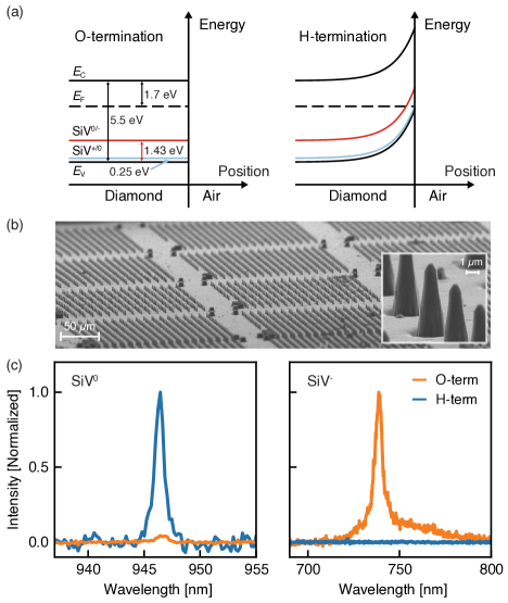
We study the charge state behavior of SiV centers in a membrane sample with a two dimensional array of PRs (Fig. 1(b)). Focusing on the photoluminescence spectrum of SiV centers in a particular PR, we observe that the emission spectrum changes drastically upon changing the chemical termination of the surface (Fig. 1(c)). Compared to the O-terminated surface, after H-termination we observe that the SiV0 emission increases while the SiV- emission decreases below background levels. We also observe formation of SiV0 in unetched regions of the membrane under H-termination (Fig. S6 [21]). Our results are consistent with prior work on H-terminated nanodiamonds where significant decrease in total SiV- fluorescence is observed after H-termination via hydrogen plasma [27]; however in prior work there has been no reported observation of SiV0. The observed emission intensity of SiV0 formed under H-termination in the uneteched region is within a factor of four of the emission intensity of SiV0 prepared in a boron doped diamond with the same implantation dose, indicating that surface control is comparably effective to bulk doping (Fig. S7(a) [21]).
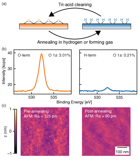
In order to preserve the properties of near-surface color centers, it is important to use a gentle surface termination procedure that avoids subsurface damage and surface roughening. To prepare an H-terminated surface, we first ensure that the diamond surface is contamination free by tri-acid cleaning, and then we anneal the sample either in hydrogen or in forming gas (Fig. 2(a)). To remove the H-termination and reset the surface to O-termination, we perform tri-acid cleaning again. X-ray photoelectron spectroscopy (XPS) shows that the oxygen 1 peak intensity decreases after hydrogen termination (Fig. 2(b)). From the inelastic mean free path of photoelectrons and the X-ray energy (1487 eV), we estimate the contribution of the signal from a monolayer of atoms on diamond surface to be 7.6% [28, 29]. Based on the oxygen 1 signal intensity observed in XPS, we conclude that the surface has 40% of a monolayer of oxygen after tri-acid cleaning while the oxygen coverage is less than 3% of a monolayer after hydrogen termination. The sub-monolayer coverage of oxygen after tri-acid cleaning is consistent with previous observations [29]. This surface termination procedure is reversible and shows consistent results over many rounds of tri-acid cleaning and hydrogen termination (Fig. S2 [21]). Atomic force microscopy (AFM) scans before and after forming gas annealing reveal that the surface remains smooth (Fig. 2(c)), making the process compatible with shallow color center applications. This is in stark contrast to the commonly used hydrogen plasma treatment where significant surface roughening, subsurface damage, or hydrogen atom diffusion may occur during the plasma treatment [30, 31, 32, 33].
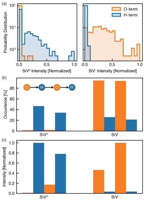
We quantify the effect of surface termination on SiV centers by measuring spectral statistics across a large number of PRs. Histograms of the SiV0 and SiV- emission intensities are dramatically different under the two different surface terminations (Fig. 3(a)). Specifically, we observe that SiV0 center emission is suppressed under O-termination while SiV- center emission is suppressed under H-termination. We iteratively prepare the surface with O-termination and H-termination and observe reversible tuning between SiV- and SiV0. We observe that both the occurrence (Fig. 3(b)) and intensity (Fig. 3(c)) toggle reversibly for SiV- and SiV0 centers. This is in contrast to plasma-based processes, where diffusion of atomic hydrogen can lead to irreversible depletion of NV centers [33]. In addition, we probe the stability of the surface against cleaning in piranha solution (a 1:2 mixture of hydrogen peroxide in concentrated sulfuric acid) and long-term air exposure. The spectral statistics of SiV centers are unchanged upon piranha cleaning (Fig. S8 [21]). In fact, we note that initial observation of SiV0 was under a surface prepared by annealing in hydrogen followed by more than 1.5 years of air exposure (Fig. S3 [21]). The stability of the charge state distribution against piranha cleaning and air exposure demonstrates the exceptional robustness of this approach.
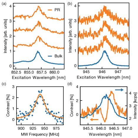
Finally, we demonstrate that SiV0 centers prepared under an H-terminated surface show similar properties to samples where SiV0 centers are formed by bulk silicon doping during growth [11, 12]. We investigate the optical transitions of SiV0 hosted in PRs prepared under an H-terminated surface using photoluminescence excitation (PLE) spectroscopy. First, we scan a narrow linewidth laser across one of the bound exciton transitions of SiV0 [12] while monitoring the emission into the zero-phonon line (ZPL) at 946 nm. A resonance around 857 nm is observed, consistent with the spectrum from a bulk doped sample, as shown in Fig. 4(a). Then, we probe the ZPL transition by scanning a narrow linewidth laser across the SiV0 ZPL while emission is measured at wavelengths longer than 960 nm. We observe a resonance at 946.2 nm, consistent with bulk PLE measurements (Fig. 4(b)).
We also observe ODMR in SiV0 centers prepared under an H-terminated surface via excitation of the ZPL transition at 946.45 nm. As the microwave (MW) frequency is swept across the zero-field splitting of SiV0, we observe a resonance peak at 940 MHz (Fig. 4(c)). In addition, we observe that the ODMR contrast at the ZPL is strongly wavelength dependent (Fig. 4(d)), suggesting that even though individual transitions are not resolvable in PLE, they are spectrally separated enough to allow spin-dependent fluorescence. The observation of ODMR in SiV0 centers via the ZPL transition is complementary to the recently demonstrated ODMR via the bound exciton transitions [12]. We note that the observed ODMR frequency of 940 MHz is slightly lower than the previously reported zero-field splitting [34], and that in this sample the ODMR frequency shifts with higher optical excitation power and MW power (Fig. S10 and Fig. S11 [21]). The origin of the shift is currently under investigation, but we note that the sign of the shift is inconsistent with heating from the microwaves or laser [34].
In conclusion, we have demonstrated that chemical control of the diamond surface can be used to tune the charge state of SiV centers to stabilize the neutral charge state in undoped diamond. The gentle surface termination procedure we developed here allows for non-destructive, reversible and long-lived control of the diamond surface. Near-surface SiV0 centers prepared using our approach preserve bulk-like optical properties and allow for optically detected magnetic resonance.
Our approach provides an alternative route to controlling color centers in diamond without careful control over the doping or defect states in the bulk. In addition, the present work focuses on static stabilization of a particular charge state. Utilizing the surface termination to control the charge state may also be compatible with dynamic electric field tuning of the Fermi level, as has been demonstrated for NV centers with electrolytic and in-plane gate electrodes [18, 19, 20]. Such an approach could be widely applicable to other color centers in diamond. For example, Fermi level tuning via surface chemical control could help stabilize and identify other neutral group IV vacancy centers, or access additional charge states of SiV (SiV+ and SiV2-), whose spectroscopic signatures have been elusive [35, 36], possibly due to challenges in Fermi level engineering. Another avenue of exploration is to control the charge transfer process by using explicit electron acceptor materials on H-terminated diamond, for example molecular species (NO2, C60 and O3 [37, 38, 39]) or solid encapsulation materials such as transition metal oxides [40].
Acknowledgements.
We gratefully acknowledge Z. Yuan for use of the visible wavelength confocal microscope and S. Mukherjee for help with surface characterization. Spectroscopy of SiV was supported by National Science Foundation through the Princeton Center for Complex Materials, a Materials Research Science and Engineering Center (Grant No. DMR-1420541) and the Air Force Office of Scientific Research under Grant No. FA9550-17-0158. Surface processing to control the charge state was supported by the U.S. Department of Energy, Office of Science, National Quantum Information Science Research Centers, Co-design Center for Quantum Advantage (C2QA) under contract number DE-SC0012704, the Swiss Nanoscience Institute and the quantERA grant SensExtreme. L.V.H.R. acknowledges support from the Department of Defense through the National Defense Science and Engineering Graduate Fellowship Program.References
- Gao et al. [2015] W. B. Gao, A. Imamoglu, H. Bernien, and R. Hanson, Coherent manipulation, measurement and entanglement of individual solid-state spins using optical fields, Nature Photonics 9, 363 (2015).
- Awschalom et al. [2018] D. D. Awschalom, R. Hanson, J. Wrachtrup, and B. B. Zhou, Quantum technologies with optically interfaced solid-state spins, Nature Photonics 12, 516 (2018).
- Atatüre et al. [2018] M. Atatüre, D. Englund, N. Vamivakas, S.-Y. Lee, and J. Wrachtrup, Material platforms for spin-based photonic quantum technologies, Nature Reviews Materials 3, 38 (2018).
- Shields et al. [2015] B. J. Shields, Q. P. Unterreithmeier, N. P. de Leon, H. Park, and M. D. Lukin, Efficient readout of a single spin state in diamond via spin-to-charge conversion, Phys. Rev. Lett. 114, 136402 (2015).
- Bourgeois et al. [2015] E. Bourgeois, A. Jarmola, P. Siyushev, M. Gulka, J. Hruby, F. Jelezko, D. Budker, and M. Nesladek, Photoelectric detection of electron spin resonance of nitrogen-vacancy centres in diamond, Nature Communications 6, 8577 (2015).
- Yuan et al. [2020] Z. Yuan, M. Fitzpatrick, L. V. H. Rodgers, S. Sangtawesin, S. Srinivasan, and N. P. de Leon, Charge state dynamics and optically detected electron spin resonance contrast of shallow nitrogen-vacancy centers in diamond, Phys. Rev. Research 2, 033263 (2020).
- Nguyen et al. [2019] C. T. Nguyen, D. D. Sukachev, M. K. Bhaskar, B. Machielse, D. S. Levonian, E. N. Knall, P. Stroganov, R. Riedinger, H. Park, M. Lončar, and M. D. Lukin, Quantum network nodes based on diamond qubits with an efficient nanophotonic interface, Phys. Rev. Lett. 123, 183602 (2019).
- Bhaskar et al. [2020] M. K. Bhaskar, R. Riedinger, B. Machielse, D. S. Levonian, C. T. Nguyen, E. N. Knall, H. Park, D. Englund, M. Lončar, D. D. Sukachev, and M. D. Lukin, Experimental demonstration of memory-enhanced quantum communication, Nature 580, 60 (2020).
- Jahnke et al. [2015] K. D. Jahnke, A. Sipahigil, J. M. Binder, M. W. Doherty, M. Metsch, L. J. Rogers, N. B. Manson, M. D. Lukin, and F. Jelezko, Electron–phonon processes of the silicon-vacancy centre in diamond, New Journal of Physics 17, 043011 (2015).
- Sukachev et al. [2017] D. D. Sukachev, A. Sipahigil, C. T. Nguyen, M. K. Bhaskar, R. E. Evans, F. Jelezko, and M. D. Lukin, Silicon-vacancy spin qubit in diamond: A quantum memory exceeding 10 ms with single-shot state readout, Phys. Rev. Lett. 119, 223602 (2017).
- Rose et al. [2018] B. C. Rose, D. Huang, Z.-H. Zhang, P. Stevenson, A. M. Tyryshkin, S. Sangtawesin, S. Srinivasan, L. Loudin, M. L. Markham, A. M. Edmonds, D. J. Twitchen, S. A. Lyon, and N. P. de Leon, Observation of an environmentally insensitive solid-state spin defect in diamond, Science 361, 60 (2018).
- Zhang et al. [2020] Z.-H. Zhang, P. Stevenson, G. Thiering, B. C. Rose, D. Huang, A. M. Edmonds, M. L. Markham, S. A. Lyon, A. Gali, and N. P. de Leon, Optically detected magnetic resonance in neutral silicon vacancy centers in diamond via bound exciton states, Phys. Rev. Lett. 125, 237402 (2020).
- Gali and Maze [2013] A. Gali and J. R. Maze, Ab initio study of the split silicon-vacancy defect in diamond: Electronic structure and related properties, Phys. Rev. B 88, 235205 (2013).
- Landstrass and Ravi [1989] M. I. Landstrass and K. V. Ravi, Resistivity of chemical vapor deposited diamond films, Applied Physics Letters 55, 975 (1989).
- Maier et al. [2000] F. Maier, M. Riedel, B. Mantel, J. Ristein, and L. Ley, Origin of surface conductivity in diamond, Physical Review Letters 85, 3472 (2000).
- Garrido et al. [2008] J. A. Garrido, S. Nowy, A. Härtl, and M. Stutzmann, The diamond/aqueous electrolyte interface: an impedance investigation, Langmuir 24, 3897 (2008).
- Hauf et al. [2011] M. V. Hauf, B. Grotz, B. Naydenov, M. Dankerl, S. Pezzagna, J. Meijer, F. Jelezko, J. Wrachtrup, M. Stutzmann, F. Reinhard, and J. A. Garrido, Chemical control of the charge state of nitrogen-vacancy centers in diamond, Phys. Rev. B 83, 081304(R) (2011).
- Grotz et al. [2012] B. Grotz, M. V. Hauf, M. Dankerl, B. Naydenov, S. Pezzagna, J. Meijer, F. Jelezko, J. Wrachtrup, M. Stutzmann, F. Reinhard, and J. A. Garrido, Charge state manipulation of qubits in diamond, Nature Communications 3, 729 (2012).
- Karaveli et al. [2016] S. Karaveli, O. Gaathon, A. Wolcott, R. Sakakibara, O. A. Shemesh, D. S. Peterka, E. S. Boyden, J. S. Owen, R. Yuste, and D. Englund, Modulation of nitrogen vacancy charge state and fluorescence in nanodiamonds using electrochemical potential, Proceedings of the National Academy of Sciences 113, 3938 (2016).
- Hauf et al. [2014] M. V. Hauf, P. Simon, N. Aslam, M. Pfender, P. Neumann, S. Pezzagna, J. Meijer, J. Wrachtrup, M. Stutzmann, F. Reinhard, and J. A. Garrido, Addressing Single Nitrogen-Vacancy Centers in Diamond with Transparent in-Plane Gate Structures, Nano Letters 14, 2359 (2014).
- [21] See Supplemental Material for experimental methods, additional characterization data and discussions.
- Evans et al. [2016] R. E. Evans, A. Sipahigil, D. D. Sukachev, A. S. Zibrov, and M. D. Lukin, Narrow-linewidth homogeneous optical emitters in diamond nanostructures via silicon ion implantation, Phys. Rev. Applied 5, 044010 (2016).
- Hedrich et al. [2020] N. Hedrich, D. Rohner, M. Batzer, P. Maletinsky, and B. J. Shields, Parabolic diamond scanning probes for single-spin magnetic field imaging, Phys. Rev. Applied 14, 064007 (2020).
- Thiering and Gali [2018] G. Thiering and A. Gali, Ab initio magneto-optical spectrum of group-iv vacancy color centers in diamond, Phys. Rev. X 8, 021063 (2018).
- Farrer [1969] R. G. Farrer, On the substitutional nitrogen donor in diamond, Solid State Communications 7, 685 (1969).
- Chrenko [1973] R. M. Chrenko, Boron, the dominant acceptor in semiconducting diamond, Physical Review B 7, 4560 (1973).
- Rogers et al. [2019] L. J. Rogers, O. Wang, Y. Liu, L. Antoniuk, C. Osterkamp, V. A. Davydov, V. N. Agafonov, A. B. Filipovski, F. Jelezko, and A. Kubanek, Single - centers in low-strain nanodiamonds with bulklike spectral properties and nanomanipulation capabilities, Phys. Rev. Applied 11, 024073 (2019).
- Shinotsuka et al. [2015] H. Shinotsuka, S. Tanuma, C. J. Powell, and D. R. Penn, Calculations of electron inelastic mean free paths. X. Data for 41 elemental solids over the 50 eV to 200 keV range with the relativistic full Penn algorithm, Surface and Interface Analysis 47, 871 (2015).
- Sangtawesin et al. [2019] S. Sangtawesin, B. L. Dwyer, S. Srinivasan, J. J. Allred, L. V. H. Rodgers, K. De Greve, A. Stacey, N. Dontschuk, K. M. O’Donnell, D. Hu, D. A. Evans, C. Jaye, D. A. Fischer, M. L. Markham, D. J. Twitchen, H. Park, M. D. Lukin, and N. P. de Leon, Origins of diamond surface noise probed by correlating single-spin measurements with surface spectroscopy, Phys. Rev. X 9, 031052 (2019).
- Koslowski et al. [1998] B. Koslowski, S. Strobel, M. J. Wenig, and P. Ziemann, Roughness transitions of diamond(100) induced by hydrogen-plasma treatment, Applied Physics A: Materials Science and Processing 66, 1159 (1998).
- Gaisinskaya et al. [2009] A. Gaisinskaya, R. Edrei, A. Hoffman, and Y. Feldheim, Morphological evolution of polished single crystal (100) diamond surface exposed to microwave hydrogen plasma, Diamond and Related Materials 18, 1466 (2009).
- Crawford et al. [2018] K. G. Crawford, A. Tallaire, X. Li, D. A. Macdonald, D. Qi, and D. A. Moran, The role of hydrogen plasma power on surface roughness and carrier transport in transfer-doped H-diamond, Diamond and Related Materials 84, 48 (2018).
- Stacey et al. [2012] A. Stacey, T. J. Karle, L. P. McGuinness, B. C. Gibson, K. Ganesan, S. Tomljenovic‐Hanic, A. D. Greentree, A. Hoffman, R. G. Beausoleil, and S. Prawer, Depletion of nitrogen‐vacancy color centers in diamond via hydrogen passivation, Applied Physics Letters 100, 071902 (2012).
- Edmonds et al. [2008] A. M. Edmonds, M. E. Newton, P. M. Martineau, D. J. Twitchen, and S. D. Williams, Electron paramagnetic resonance studies of silicon-related defects in diamond, Phys. Rev. B 77, 245205 (2008).
- Krivobok et al. [2020] V. S. Krivobok, E. A. Ekimov, S. G. Lyapin, S. N. Nikolaev, Y. A. Skakov, A. A. Razgulov, and M. V. Kondrin, Observation of a 1.979-eV spectral line of a germanium-related color center in microdiamonds and nanodiamonds, Physical Review B 101, 144103 (2020).
- Lühmann et al. [2020] T. Lühmann, J. Küpper, S. Dietel, R. Staacke, J. Meijer, and S. Pezzagna, Charge-State Tuning of Single SnV Centers in Diamond, ACS Photonics 7, 3376 (2020).
- Sato and Kasu [2013] H. Sato and M. Kasu, Maximum hole concentration for Hydrogen-terminated diamond surfaces with various surface orientations obtained by exposure to highly concentrated NO2, Diamond and Related Materials 31, 47 (2013).
- Kubovic and Kasu [2010] M. Kubovic and M. Kasu, Enhancement and stabilization of hole concentration of hydrogen-terminated diamond surface using ozone adsorbates, Japanese Journal of Applied Physics 49, 110208 (2010).
- Strobel et al. [2004] P. Strobel, M. Riedel, J. Ristein, and L. Ley, Surface transfer doping of diamond, Nature 430, 439 (2004).
- Russell et al. [2013] S. A. O. Russell, L. Cao, D. Qi, A. Tallaire, K. G. Crawford, A. T. S. Wee, and D. A. J. Moran, Surface transfer doping of diamond by MoO3: A combined spectroscopic and Hall measurement study, Applied Physics Letters 103, 202112 (2013).