Thermal spin current generation in the multifunctional ferrimagnet Ga0.6Fe1.4O3
Abstract
In recent years, multifunctional materials have attracted increasing interest for magnetic memories and energy harvesting applications. Magnetic insulating materials are of special interest for this purpose, since they allow the design of more efficient devices due to the lower Joule heat losses. In this context, Ga0.6Fe1.4O3 (GFO) is a good candidate for spintronics applications, since it can exhibit multiferroicity and presents a spin Hall magnetoresistance similar to the one observed in a yttrium iron garnet (YIG)/Pt bilayer. Here, we explore GFO utilizing thermo-spin measurements in an on-chip approach. By carefully considering the geometry of our thermo-spin devices we are able to quantify the spin Seebeck effect and the spin current generation in a GFO/Pt bilayer, obtaining a value comparable to that of YIG/Pt. This further confirms the promises of an efficient spin current generation with the possibility of an electric-field manipulation of the magnetic properties of the system in an insulating ferrimagnetic material.
I Introduction
The search for multifunctional materials is nowadays a hot topic in spintronics[1, 2]. Currently, functional devices are typically made of a bilayer composed of a non-magnetic material with large spin-orbit coupling (NM) and a ferromagnetic material (FM). These types of devices allow functionalities such as the manipulation of the FM magnetization by the spin Hall effect (SHE)[3, 4, 5] in the NM or energy harvesting by employing its inverse counterpart, the inverse spin Hall effect[6]. Insulating magnetic materials (FMI) are preferred for this purpose to pave the way towards low dissipation spintronics devices[3]. Additional functionalities like the possibility of the electric field control of the magnetic properties of such systems could be given to these heterostructures by the introduction of multifunctional magnetic materials, opening the possibility of designing more efficient and versatile devices[7, 8].
In spin Seebeck experiments[9, 10, 11, 12] a thermal gradient is typically applied in the out-of-plane direction of the magnetic thin film, generating a spin current flowing alongside this direction. In insulating ferromagnetic materials, this spin current is carried by spin collective excitations, also called magnons, and can be injected into an adjacent layer such as Pt in the case of this study, and is then converted into a charge current via the inverse spin Hall effect (ISHE)[13, 14, 15]. This conversion occurs through the spin-orbit interaction of conduction electrons, which can be strong in heavy metals like Pt and is given by[16]:
| (1) |
where is the electric field produced by the ISHE, and are the electron charge and reduced Plank constant, is the resistivity of the Pt layer, is the spin Hall angle, is the spin current injected into Pt and its spin polarization.
Until now, yttrium iron garnet (YIG) has been the cornerstone material in thermo-spin phenomena due to its insulating nature and its unique magnetic properties such as low damping and coercive field. Here, we have studied the thermo-spin current generation in bilayers composed of Pt and the multifunctional magnetoelectric oxide Ga0.6Fe1.4O3 (GFO)[17, 18]. Engineering of thermo-spin devices with properly chosen dimensions allowed an accurate determination of the thermo-spin voltages necessary to calculate the spin Seebeck coefficient, and therefore granting a comparison with other systems. Indeed, the spin Seebeck effect (SSE) as well the spin Hall magnetoresistance [19, 20, 21] in GFO system are largely comparable with YIG-based ones. Furthemore, to corroborate our experimental finding we resorted to finite element simulations of the thermal profile to obtain an accurate heat flux in both GFO and YIG layers.
II Methods
II.1 Growth and structural characterization
GFO films were prepared by pulsed laser deposition (PLD) on SrTiO3(111) substrates (Furuuchi Chemical Corporation, Japan, with root mean square roughness lower than 0.15 nm) maintained at 900°C. The KrF excimer laser ( = 248 nm) was operated with a fluence of 4 J/cm2 [21] and a repetition rate of 2 Hz. The growth was done from a stoichiometric GFO target in an atmosphere of 0.1 mBar of O2. The YIG film was grown by liquid phase epitaxy on 3-inch (111)-oriented gadolinium gallium garnet (GGG) substrate from PbO-B2O3-based high-temperature solution (HTL) at about 800°C using a standard dipping technique [22, 23]. During the deposition time of 90 seconds, the substrate was rotated in the solution at 33 rpm and then pulled out. Subsequently, the solution residues were spun off from the sample surface above the HTL and the sample was pulled out of the hot heating zone. Platinum layers for the GFO-based samples were deposited by PLD in situ in order to avoid any surface contamination. The deposition was carried out at room temperature in order to avoid any metal/oxide interdiffusion, under vacuum (base pressure of 2 x 10⁻⁸ mbar) and with a deposition rate of 0.06 nm/s, as in [21].
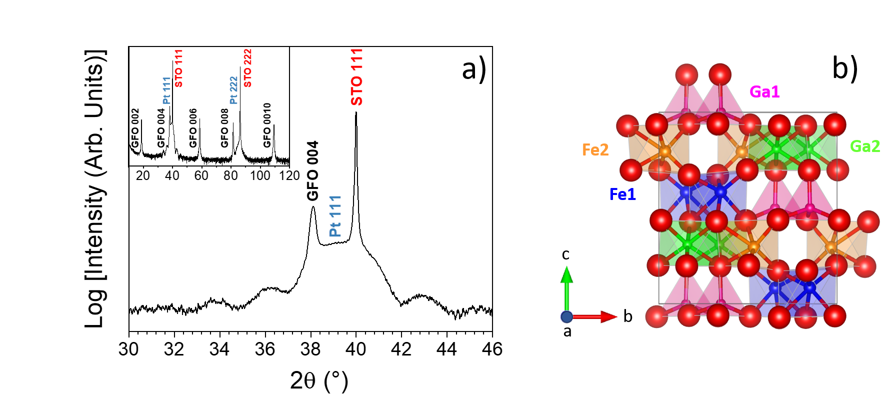
Structural characterization of the samples was done by X-ray diffraction scans using a Rigaku Smart Lab diffractometer equipped with a rotating anode (9 kW) and monochromated copper radiation (1.54056 Å). The scan shown in figure 1 indicates that the system grows following the (SrTiO3) STO(111)//GFO(001)/Pt(111) structure, i.e., with the GFO film oriented along the [001] direction. The presence of Laue oscillations for the Pt (111) reflection is an indication of a smooth Pt/GFO interface.
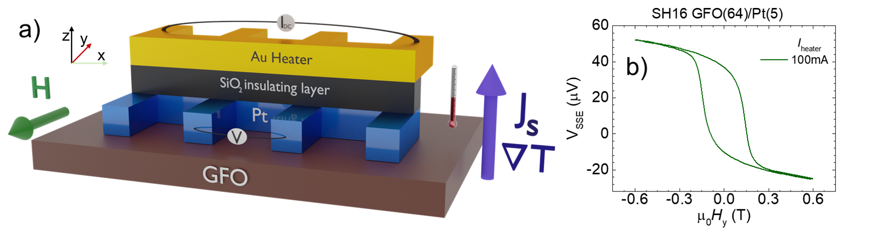
The thermo-spin devices were made using conventional UV lithography. We have chosen the following stacking to perform our main experiments: STO//GFO(64 nm)/Pt(5 nm) and GGG//YIG(140 nm)/Pt(5 nm). The Pt thin film is first patterned by ion milling. Then, an insulating SiO2 layer with a thickness of 75 nm is grown by RF sputtering using a Si target and Ar+ and O2- plasma. In a third and last step the Au heater (Ti(10 nm)/Au(150 nm)) is evaporated using a conventional evaporator. Both the heater and the sample are patterned with four pads to measure their resistance using four probes for more precise estimation. The dimensions of the active part of the heater and the sample are 33010 m2 and 27010 m2 respectively.
II.2 Thermo-spin measurements and estimation of heat transport parameters
Thermo-spin measurements are carried out in these devices using an electromagnet to apply an external in-plane magnetic field (H) as shown in figure 2 (a). A DC current is passed through the heater and after 5 minutes of stabilization, the resistances of the sample and the heater are monitored using I-V measurements to avoid spurious contributions from thermal voltages. The thermo-spin voltage is monitored using a Keithley 2182a nano voltmeter.
Numerical simulations based on finite element method have been performed by COMSOL multiphysics, coupling the Electric Currents and Heat Transfer modules, in order to quantify thermal gradients in GFO on STO substrate and in YIG on GGG substrate (see supporting information). The cross-plane thermal conductivity of the GFO thin film was measured using the 3 method. In this method a thin metal resistor simultaneously serves as a heater and a thermometer, it has been previously employed to determine the thermal conductivity of bulk and thin film materials, details of the measurements can be found elsewhere [24, 25, 26]. For these measurements a Pt resistor (100 nm thick, 10 um width, 1 mm length with 10 nm of Cr for adhesion) is deposited on the bare GFO/STO heterostructure and the 3 voltage response to an AC current with frequency is measured. The thermal parameters of the other layers are obtained from literature[27, 28, 29, 30, 31, 32, 33] and detailed in the supporting information.
III Results
III.1 Thermo-spin voltage in GFO/Pt and YIG/Pt
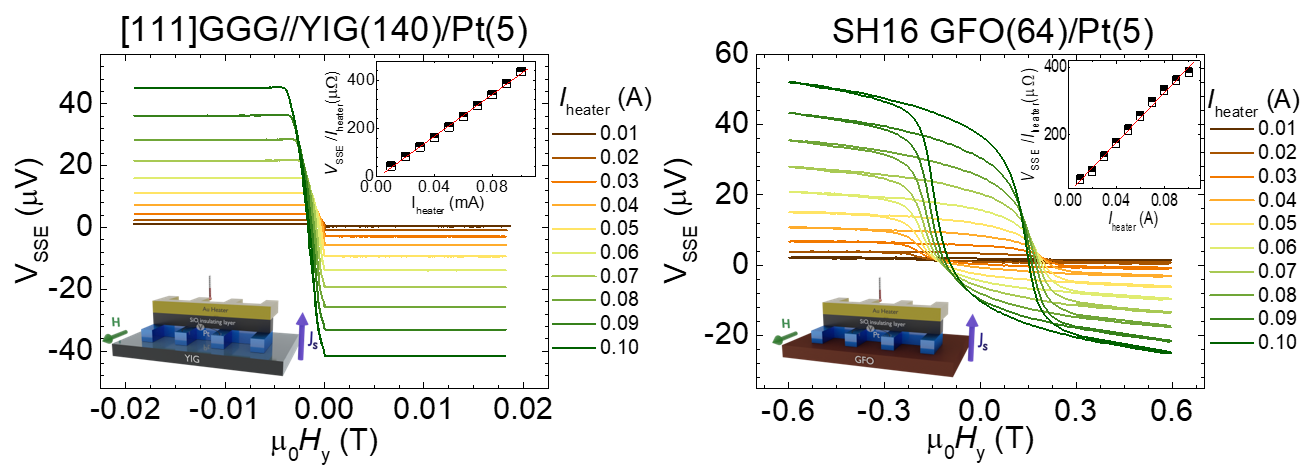
We have performed thermo-spin measurements in a GFO/Pt and YIG/Pt systems by observing the thermally induced voltage upon sweeping H as shown in figure 2(a) for GFO, obtaining a typical hysteresis loop-like curve that follows the magnetization of the GFO thin film[21] (figure 2(b)) for a heater current of 100 mA. We have performed these measurements for H applied at different directions in YIG and GFO and observed an isotropic behaviour of the SSE voltage.
By monitoring the magnitude of the thermo-spin voltage at saturation for different heater powers we can observe that the voltage difference between the saturation at positive and negative fields scales linearly with the power applied to the heater, as expected by the origin of the spin current generated in GFO. This is shown in the insets of figure 3 for both GFO and YIG systems. We also observe here that the order of magnitude of the SSE voltage is similar in both systems, although in the GFO the offset voltage of the loop and the coercive field are significantly larger than in YIG. While the elucidation of the origin of such offset voltage is out of the scope of this paper, we argue that it might be related to a persistent pyroelectric current due to the polar nature of the GFO[34].
III.2 Quantitative comparison of the spin Seebeck effect in YIG and GFO
The determination of the spin Seebeck coefficient is normally subjected to large uncertainty due to the low reproducibility of the experimental conditions. Typically, in literature, the SSE coefficient is defined as the ratio between the SSE voltage and the thermal gradient in the FM thin film normalized by the sample resistance[35].
| (2) |
where VISHE is the thermo-spin voltage difference between positive and negative saturation fields divided by two, T is the thermal gradient through the FMI, RPt is the 4-probe resistance in the Pt using I-V measurements and l is the distance between the voltage contacts.
Two steps can be taken to overcome the issue of low reproducibility in SSE measurements: first, the heat flux in the system can be considered instead of an estimation of the thermal gradient[36], and second, it is possible to maximize the reproducibility of the thermal conditions by using on-chip devices for a consistent thermal contact and dimensions of the system[37, 38, 39].
Following both of these steps, we propose to define the SSE coefficient considering the heat flux instead of the thermal gradient in the FMI (S) as follows:
| (3) |
where is the heat flux through the FMI.
To reliably compare the thermo-spin voltage in the GFO/Pt and YIG/Pt systems we compute the S from equation 3 and obtain a comparable value for both systems as depicted in table 1. We obtain a S= 2.90.3 for GFO, whereas for YIG the value is slighty larger, 3.60.4. This suggests that the efficiency of the spin current generation in GFO is similar to that of YIG, opening new possibilities in spin caloritronics using insulating magnetic materials with predicted tunable magnetic properties by electric fields.
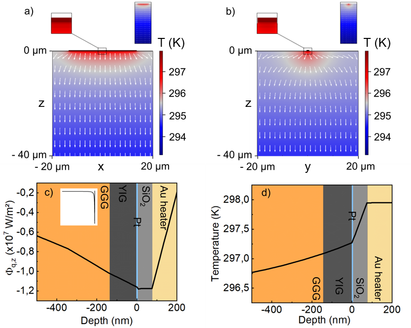
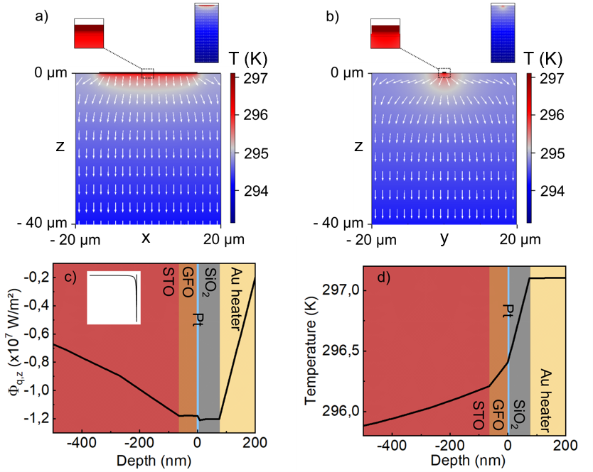
Using the thermal conductivity for both FMI we can also estimate the thermal gradient in the FMI layers considering Fourier’s law and a one-dimensional thermal flux () to compare with other studies in literature as shown in table 1. We observe that the temperature difference between the upper and lower boundaries of the FMI in both systems are similar in magnitude under these considerations. To assess possible deviations from this simplified model due to the geometry of the device and possible thermal losses, we have performed a finite element simulation using COMSOL. In this simulation, we introduce the geometry of the system and use a combination of the electric currents and heat transfer modules and we obtain a temperature difference in the FMI layer slightly smaller but comparable to the one calculated by Fourier’s law for both systems. Figures 4(a) and (b) show respectively the local temperature distribution in the device in both X0Z and 0YZ cut planes. They show that the temperature gradient direction is mostly out of plane within the device, as expected. The heat flux through the GFO layer is almost constant as shown in figure 4(c) indicating that the thermal losses are not relevant and the direction of the thermal gradient is almost completely out of plane in the GFO. Figure 4(d) shows the simulated thermal profile in the whole device.
| (cm) | S () | (W/mK) | (K) | (K) | S () | |
|---|---|---|---|---|---|---|
| GFO/Pt | 27.5 | 2.90.3 | 4 1 | 0.251 | 0.191 | 90 10 |
| YIG/Pt | 25.3 | 3.60.4 | 8.5 | 0.252 | 0.190 | 160 20 |
In the case of GFO, we have estimated the thermal conductivity using the 3 method to be W/mK, significantly smaller than that of YIG[27]. The rest of the values considered have been extracted from literature [27, 28, 29, 30, 30, 31, 32, 33]. Following these estimations, the value of the SSE considering the thermal gradient in the FMI can be recovered to compare with other studies. The calculated values of S are 9010 and 16020 respectively. The rest of the parameters to obtain them are shown in table 1. We obtain a value of S within the same order of magnitude and a similar value of S for both materials, showing that for both methods of estimating the spin current generation point towards the interest in using GFO as a promising functional material in insulating spintronics.
IV Conclusions
In summary, we have explored the thermo-spin properties of the multi-functional material Ga0.6Fe1.4O3 in the form of thin film for energy harvesting and thermal management applications. This material provides additional functionality in terms of ferroelectricity while maintaining the electrically insulating behaviour compared to other materials such as yttrium iron garnet. By using an on-chip approach to increase reproducibility and carefully considering the heat flux and thermal gradients in both systems, we find that the spin current generation by thermal excitation is comparable to the one of yttrium iron garnet. This observation supports the promises of an efficient spin current generation with the possibility of an electric-field manipulation of the magnetic properties of the system in a new insulating ferrimagnetic material. Our results show that this material can be exploited in spintronics and spin caloritronics applications.
Acknowledgements.
This work was funded by the French National Research Agency (ANR) through the ANR-18-CECE24-0008-01 ‘ANR MISSION’ and the No. ANR-19-CE24-0016-01 ‘Toptronic ANR’. S.H. acknowledges the Interdisciplinary Thematic Institute QMat, as part of the ITI 2021 2028 program of the University of Strasbourg, CNRS and Inserm, supported by IdEx Unistra (ANR 10 IDEX 0002), SFRI STRAT’US project (ANR 20 SFRI 0012), ANR-11-LABX-0058 NIE, and ANR-17-EURE-0024 under the framework of the French Investments for the Future Program. M. L. acknowledges the funding by the German Bundesministerium für Wirtschaft und Energie (BMWi) - 49MF180119. R.R. acknowledges support from the European Commission through the project 734187-SPICOLOST (H2020-MSCA-RISE-2016), the European Union’s Horizon 2020 research and innovation programme through the MSCA grant agreement SPEC-894006, Grant RYC 2019-026915-I funded by the MCIN/AEI/10.13039/501100011033 and by “ESF investing in your future”, the Xunta de Galicia (ED431B 2021/013, Centro Singular de Investigación de Galicia Accreditation 2019-2022, ED431G 2019/03) and the European Union (European Regional Development Fund - ERDF). We also thank B. Wenzel, R. Meyer, M. Reich and O. Surzhenko (INNOVENT) for their support.References
- Eerenstein et al. [2006] W. Eerenstein, N. Mathur, and J. F. Scott, Nature 442, 759 (2006).
- Scott [2007] J. Scott, Nature Materials 6, 256 (2007).
- Avci et al. [2017] C. O. Avci, A. Quindeau, C.-F. Pai, M. Mann, L. Caretta, A. S. Tang, M. C. Onbasli, C. A. Ross, and G. S. Beach, Nature Materials 16, 309 (2017).
- Garello et al. [2014] K. Garello, C. O. Avci, I. M. Miron, M. Baumgartner, A. Ghosh, S. Auffret, O. Boulle, G. Gaudin, and P. Gambardella, Applied Physics Letters 105, 212402 (2014).
- Anadon et al. [2020] A. Anadon, R. Guerrero, J. A. Jover-Galtier, A. Gudin, J. M. Diez Toledano, P. Olleros-Rodriguez, R. Miranda, J. Camarero, and P. Perna, ACS Applied Nano Materials 4, 487 (2020).
- Ramos et al. [2016] R. Ramos, A. Anadón, I. Lucas, K. Uchida, P. Algarabel, L. Morellón, M. Aguirre, E. Saitoh, and M. Ibarra, APL Materials 4, 104802 (2016).
- Manipatruni et al. [2019] S. Manipatruni, D. E. Nikonov, C.-C. Lin, T. A. Gosavi, H. Liu, B. Prasad, Y.-L. Huang, E. Bonturim, R. Ramesh, and I. A. Young, Nature 565, 35 (2019).
- Ramesh [2009] R. Ramesh, Nature 461, 1218 (2009).
- Uchida et al. [2014a] K. Uchida, M. Ishida, T. Kikkawa, A. Kirihara, T. Murakami, and E. Saitoh, Journal of Physics: Condensed Matter 26, 343202 (2014a).
- Anadón et al. [2021] A. Anadón, A. Gudín, R. Guerrero, I. Arnay, A. Guedeja-Marron, P. Jiménez-Cavero, J. M. Díez Toledano, F. Ajejas, M. Varela, S. Petit-Watelot, et al., APL Materials 9, 061113 (2021).
- Uchida et al. [2010] K.-i. Uchida, J. Xiao, H. Adachi, J.-i. Ohe, S. Takahashi, J. Ieda, T. Ota, Y. Kajiwara, H. Umezawa, H. Kawai, et al., Nature Materials 9, 894 (2010).
- ichi Uchida et al. [2016] K. ichi Uchida, H. Adachi, T. Kikkawa, A. Kirihara, M. Ishida, S. Yorozu, S. Maekawa, and E. Saitoh, Proceedings of the IEEE (2016), 10.1109/JPROC.2016.2535167, arXiv:1604.00477 .
- Hoffmann [2013] A. Hoffmann, IEEE transactions on magnetics 49, 5172 (2013).
- Sinova et al. [2015] J. Sinova, S. O. Valenzuela, J. Wunderlich, C. Back, and T. Jungwirth, Reviews of Modern Physics 87, 1213 (2015).
- Rezende et al. [2014] S. M. Rezende, R. L. Rodríguez-Suárez, R. O. Cunha, A. R. Rodrigues, F. L. A. Machado, G. A. Fonseca Guerra, J. C. Lopez Ortiz, and A. Azevedo, Physical Review B 89, 014416 (2014).
- Kikkawa et al. [2021] T. Kikkawa, D. Reitz, H. Ito, T. Makiuchi, T. Sugimoto, K. Tsunekawa, S. Daimon, K. Oyanagi, R. Ramos, S. Takahashi, Y. Shiomi, Y. Tserkovnyak, and E. Saitoh, Nature Communications 12, 4356 (2021).
- Roy et al. [2014] A. Roy, S. Mukherjee, R. Gupta, R. Prasad, and A. Garg, Ferroelectrics 473, 154 (2014).
- Stoeffler [2012] D. Stoeffler, Journal of Physics: Condensed Matter 24, 185502 (2012).
- Althammer et al. [2013] M. Althammer, S. Meyer, H. Nakayama, M. Schreier, S. Altmannshofer, M. Weiler, H. Huebl, S. Geprägs, M. Opel, R. Gross, D. Meier, C. Klewe, T. Kuschel, J.-M. Schmalhorst, G. Reiss, L. Shen, A. Gupta, Y.-T. Chen, G. E. W. Bauer, E. Saitoh, and S. T. B. Goennenwein, Physical Review B 87, 224401 (2013).
- Nakayama et al. [2013] H. Nakayama, M. Althammer, Y.-T. Chen, K. Uchida, Y. Kajiwara, D. Kikuchi, T. Ohtani, S. Geprägs, M. Opel, S. Takahashi, R. Gross, G. E. W. Bauer, S. T. B. Goennenwein, and E. Saitoh, Physical Review Letters 110, 206601 (2013).
- Homkar et al. [2021] S. Homkar, E. Martin, B. Meunier, A. Anadon-Barcelona, C. Bouillet, J. Gorchon, K. Dumesnil, C. Lefèvre, F. Roulland, O. Copie, et al., ACS Applied Electronic Materials (2021).
- Giess [1975] E. Giess, in Vapour Growth and Epitaxy (Elsevier, 1975) pp. 358–365.
- Dubs et al. [2017] C. Dubs, O. Surzhenko, R. Linke, A. Danilewsky, U. Brückner, and J. Dellith, Journal of Physics D: Applied Physics 50, 204005 (2017).
- Cahill [1990] D. G. Cahill, Review of Scientific Instruments 61, 802 (1990).
- Langenberg et al. [2016] E. Langenberg, E. Ferreiro-Vila, V. Leborán, A. O. Fumega, V. Pardo, and F. Rivadulla, APL Materials 4, 104815 (2016), https://doi.org/10.1063/1.4966220 .
- Jiménez-Cavero et al. [2021] P. Jiménez-Cavero, I. Lucas, D. Bugallo, C. López-Bueno, R. Ramos, P. A. Algarabel, M. R. Ibarra, F. Rivadulla, and L. Morellón, Applied Physics Letters 118, 092404 (2021), https://doi.org/10.1063/5.0038192 .
- Euler et al. [2015] C. Euler, P. Hołuj, T. Langner, A. Kehlberger, V. I. Vasyuchka, M. Kläui, and G. Jakob, Phys. Rev. B 92, 094406 (2015).
- Boona and Heremans [2014] S. R. Boona and J. P. Heremans, Physical Review B 90, 064421 (2014).
- Suemune [1965] Y. Suemune, Journal of the Physical Society of Japan 20, 174 (1965).
- Bussmann-Holder [2019] A. Bussmann-Holder, Ferroelectrics 553, 26 (2019).
- de Ligny and Richet [1996] D. de Ligny and P. Richet, Physical Review B 53, 3013 (1996).
- Wang et al. [2008] B. Wang, H. Jiang, X. Jia, Q. Zhang, D. Sun, and S. Yin, Frontiers of Optoelectronics in China 1, 138 (2008).
- Samoshkin and Stankus [2020] D. A. Samoshkin and S. V. Stankus, Journal of Physics: Conference Series 1677, 012175 (2020).
- Katayama et al. [2018] T. Katayama, S. Yasui, Y. Hamasaki, T. Shiraishi, A. Akama, T. Kiguchi, and M. Itoh, Advanced Functional Materials 28, 1704789 (2018), https://onlinelibrary.wiley.com/doi/pdf/10.1002/adfm.201704789 .
- Rezende et al. [2018] S. M. Rezende, A. Azevedo, and R. L. Rodriguez-Suárez, Journal of Physics D: Applied Physics 51 (2018), 10.1088/1361-6463/aab5f8.
- Sola et al. [2017] A. Sola, P. Bougiatioti, M. Kuepferling, D. Meier, G. Reiss, M. Pasquale, T. Kuschel, and V. Basso, Scientific Reports 7, 46752 (2017), arXiv:1701.03285 .
- Wu et al. [2015a] S. M. Wu, F. Y. Fradin, J. Hoffman, A. Hoffmann, and A. Bhattacharya, Journal of Applied Physics 117, 17C509 (2015a).
- Luo et al. [2021] Y. Luo, C. Liu, H. Saglam, Y. Li, W. Zhang, S. S.-L. Zhang, J. E. Pearson, B. Fisher, T. Zhou, A. Bhattacharya, and A. Hoffmann, Phys. Rev. B 103, L020401 (2021).
- Liu et al. [2021] C. Liu, Y. Luo, D. Hong, S. S.-L. Zhang, H. Saglam, Y. Li, Y. Lin, B. Fisher, J. E. Pearson, J. S. Jiang, H. Zhou, J. Wen, A. Hoffmann, and A. Bhattacharya, Science Advances 7, eabg1669 (2021), https://www.science.org/doi/pdf/10.1126/sciadv.abg1669 .
- Guillemard et al. [2018] C. Guillemard, S. Petit-Watelot, S. Andrieu, and J.-C. Rojas-Sánchez, Applied Physics Letters 113, 262404 (2018), https://doi.org/10.1063/1.5079236 .
- Wu et al. [2015b] S. M. Wu, F. Y. Fradin, J. Hoffman, A. Hoffmann, and A. Bhattacharya, Journal of Applied Physics 117, 17C509 (2015b), 1501.07599 .
- Uchida et al. [2014b] K. Uchida, M. Ishida, T. Kikkawa, a. Kirihara, T. Murakami, and E. Saitoh, Journal of physics. Condensed matter : an Institute of Physics journal 26, 343202 (2014b).
Supporting information
IV.1 Methods
| t (nm) | (W/mK) | Cp (J/KgK) | (Kg/m3) | |
|---|---|---|---|---|
| GFO | 64 | 41 (this paper) | 680* | 5 530 |
| YIG | 140 | 8.5[27] | 600[28] | 5 170 |
| STO | 100000 | 12[29, 30] | 437[30, 31] | 4 891 |
| GGG | 100000 | 7.5[32] | 380[33] | 7 080 |
| SiO2 | 75 | 1.3 | 680 | 2 270 |
| Pt | 5 | 69.1 | 130 | 21 450 |
| Au | 150 | 310 | 130 | 19 300 |
| Air | 225 | 0.0262 | 1 003 | 1.225 |
Thermal gradients were calculated in GFO on STO substrate and in YIG on GGG substrate by finite element method (FEM) simulations in COMSOL Multiphysics software by coupling Electric Currents and Heat transfer modules. An electric current density jc= 610 A/m2 flows into the Au wire while temperature is fixed at 293.15 K on the bottom of the substrate. We used thermal insulation condition on all the external boundaries (except the one whose temperature is fixed at room temperature) and thin layer condition for the Pt layer. We considered a Pt(5 nm) / SiO2(75 nm) / Au(150 nm) wire (27 x 1 um²) on either GGG (100 m) / YIG (140 nm) or STO (100 m) / GFO (64 nm). All the parameters of interest for each material are indicated in table S1.
IV.2 Finite element simulation of the thermal profile in YIG
A finite element simulation was also carried out using the parameters of the YIG/Pt sample as shown in table S1. The resulting thermal and heat flux profiles are similar to the ones in GFO and can be observed in figure S1.