Intertwining of magnetism and charge ordering
in kagome FeGe
Abstract
Recent experiments report a charge density wave (CDW) in the antiferromagnet FeGe, but the nature of the charge ordering and the associated structural distortion remains elusive. We discuss the structural and electronic properties of FeGe. Our proposed ground state phase accurately captures atomic topographies acquired by scanning tunneling microscopy. We show that the 221 CDW likely results from the Fermi surface nesting of hexagonal-prism-shaped kagome states. FeGe is found to exhibit distortions in the positions of the Ge atoms instead of the Fe atoms in the kagome layers. Using in-depth first-principles calculations and analytical modeling, we demonstrate that this unconventional distortion is driven by the intertwining of magnetic exchange coupling and CDW interactions in this kagome material. Movement of Ge atoms from their pristine positions also enhances the magnetic moment of the Fe kagome layers. Our study indicates that magnetic kagome lattices provide a material candidate for exploring the effects of strong electronic correlations on the ground state and their implications for transport, magnetic, and optical responses in materials.
KEYWORDS: kagome antiferromagnet, charge density wave, intertwined orders, first-principles calculations, crystal structure, electronic properties
1 Introduction
Density wave orders in two-dimensional and layered materials are known to exhibit rich interplay with their underlying lattice motifs1, 2, 3, 4, 5, 6, 7, 8, 9, 10, 11, 12, 13. For example, the honeycomb lattice exhibits the kekulé bond-density-wave order1, 2. In graphene, such kekulé order can give rise to massive Dirac fermions via chiral symmetry breaking, a mechanism analogous to dynamical mass generation of fundamental fermions in the Standard Model 3. Similarly, the kagome lattice supports a rich tapestry of charge density wave (CDW) orders 6, 7, 8, 9, 10, 11, 12, 13. In KV3Sb5, the CDW is associated with time-reversal-breaking orbital current order, closely related to the Haldane model for Chern insulators and the Varma model for the cuprate superconductors 14. The exploration of new quantum materials exhibiting density wave orders under broken time-reversal symmetry, especially in the honeycomb and kagome lattices, promises the discovery of exotic many-body quantum phases, including the exotic orbital current orders15, unconventional topological superconductors14, 16, 17 and phases supporting fractional excitations 1.
The antiferromagnet FeGe assumes a crystal structure comprised of alternating honeycomb and kagome atomic layers. Recent neutron scattering, spectroscopy and transport measurements suggest a CDW in FeGe, providing an example of a CDW in a kagome magnet 18, 19. However, the nature of the structural distortion and the mechanism driving the CDW remain elusive. Here, by analyzing in-depth first-principles calculations with optimized atomic structure, we predict that FeGe hosts an unusual hybrid kagome-honeycomb CDW. We find a CDW, which takes the form of a generalized kekulé distortion of the Ge honeycomb layers, while the Fe kagome layers almost remain unchanged. Our analysis indicates that the honeycomb generalized kekulé distortion is likely to be driven by the Fermi surface nesting of kagome electronic states. Our predicted honeycomb-kagome CDW is further substantiated by the matching with the atomic distribution of the electronic density of states data obtained via scanning tunneling microscopy (STM).
1.1 Results and discussion
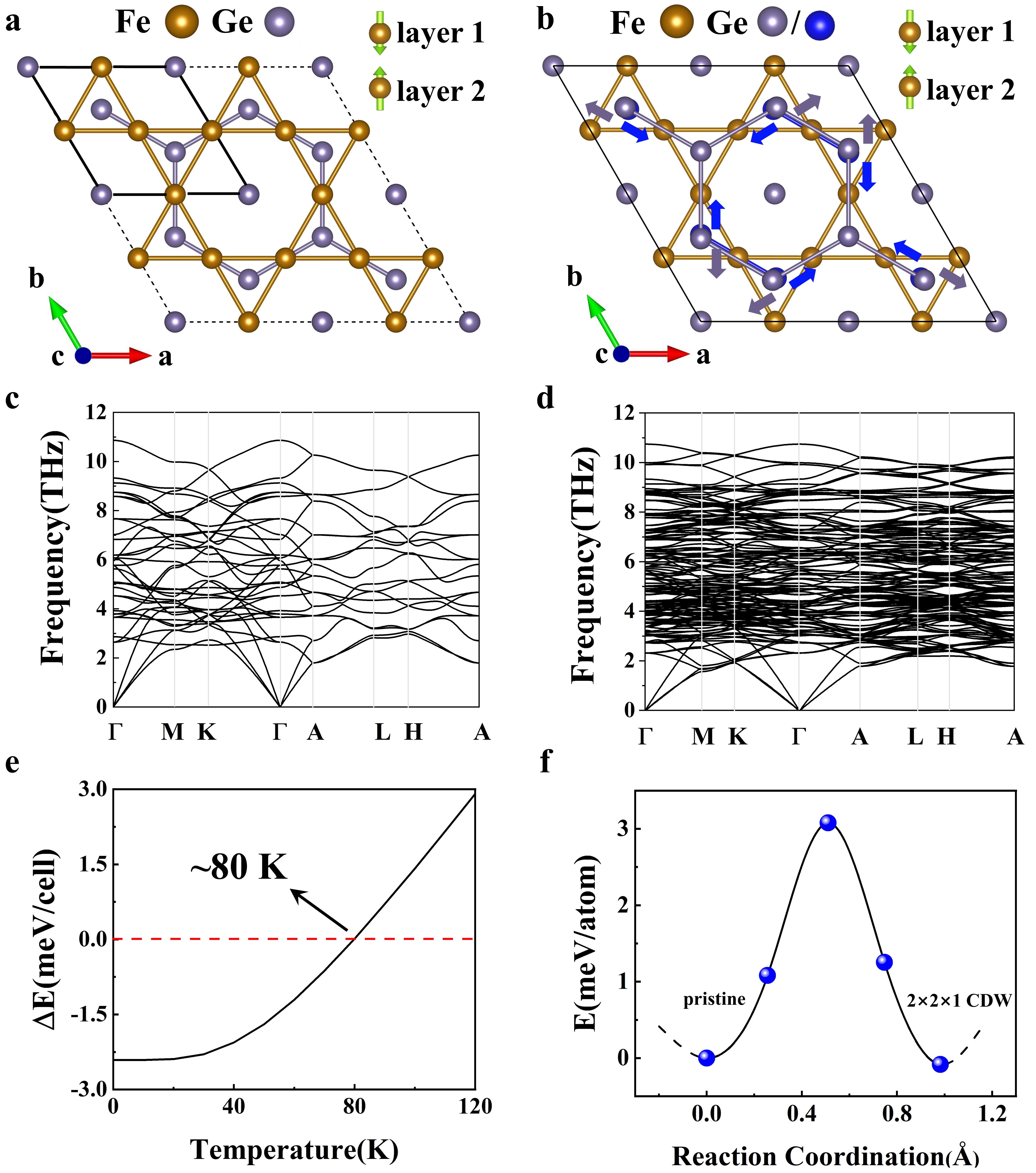
The pristine phase of FeGe is in the space group (No.191) [Figure 1a], where Fe atoms form kagome layers. There are two types of Ge atoms, one is located at the hexagonal center of the Fe kagome layer and the other forms honeycomb layers located in between the two kagome layers. Our calculation shows that the pristine phase is inter-layer antiferromagnetic with magnetic moment perpendicular to the kagome layer. By using the high-performance structure research software CALYPSO20, 21, 22, we identify four types of antiferromagnetic FeGe supercell structures (Note 1 in Supporting Information). Among these, the 221 and 222 supercell structures are the lowest energy structures that compete with the pristine phase after the zero-point energy is included. This is consistent with experimental results18, 19, where the 221 and 222 CDW interactions have been reported. Our ground state 221 structures are shown in Figure 1b. The 221 structure shares the space group with the pristine phase. Arrows indicate the movement of atoms in the supercell in the ab-plane. The Fe kagome layers are seen to be almost unchanged. The Ge atoms, which form the honeycomb lattice in different layers, move in opposite directions. As a result of this distortion, we have two inequivalent Fe atoms and six inequivalent Ge atoms in the 221 supercell.
To understand the transition between the phases, we plot the computed phonon band structure of the pristine and the 221 CDW phase in Figure 1c,d, respectively. Both these phases are seen to be dynamically stable. This should be contrasted sharply with most of the previously reported materials, which display a CDW phase transition, where the phonon spectrum of the pristine phase exhibits a softening mode at low temperature26, 27, 28, 29. To further understand the nature of the phase transition, we consider the Gibbs free energy of 221 CDW phase relative to the pristine phase, which is expected to increase with increasing temperature (Figure 1e). At low temperatures, the energy difference is negative, but it changes sign at 80 K, where the phase transition takes place. This is close to the results of the latest experiments18, 19, where the CDW transition is reported at 100-110 K. We further consider the energy barrier in the reaction pathway between the pristine and the 221 CDW phase in Figure 1f, where both phases are local minima in energy and the CDW phase shows slightly lower energy. There is an energy barrier of 3.06 meV/atom along the reaction path. This is different from the case of the kagome family AV3Sb5 (A = K, Rb, Cs) 11, where the pristine phase sits at a saddle point of a potential energy surface, so that the softening mode will trigger a spontaneous change to a lower energy phase.
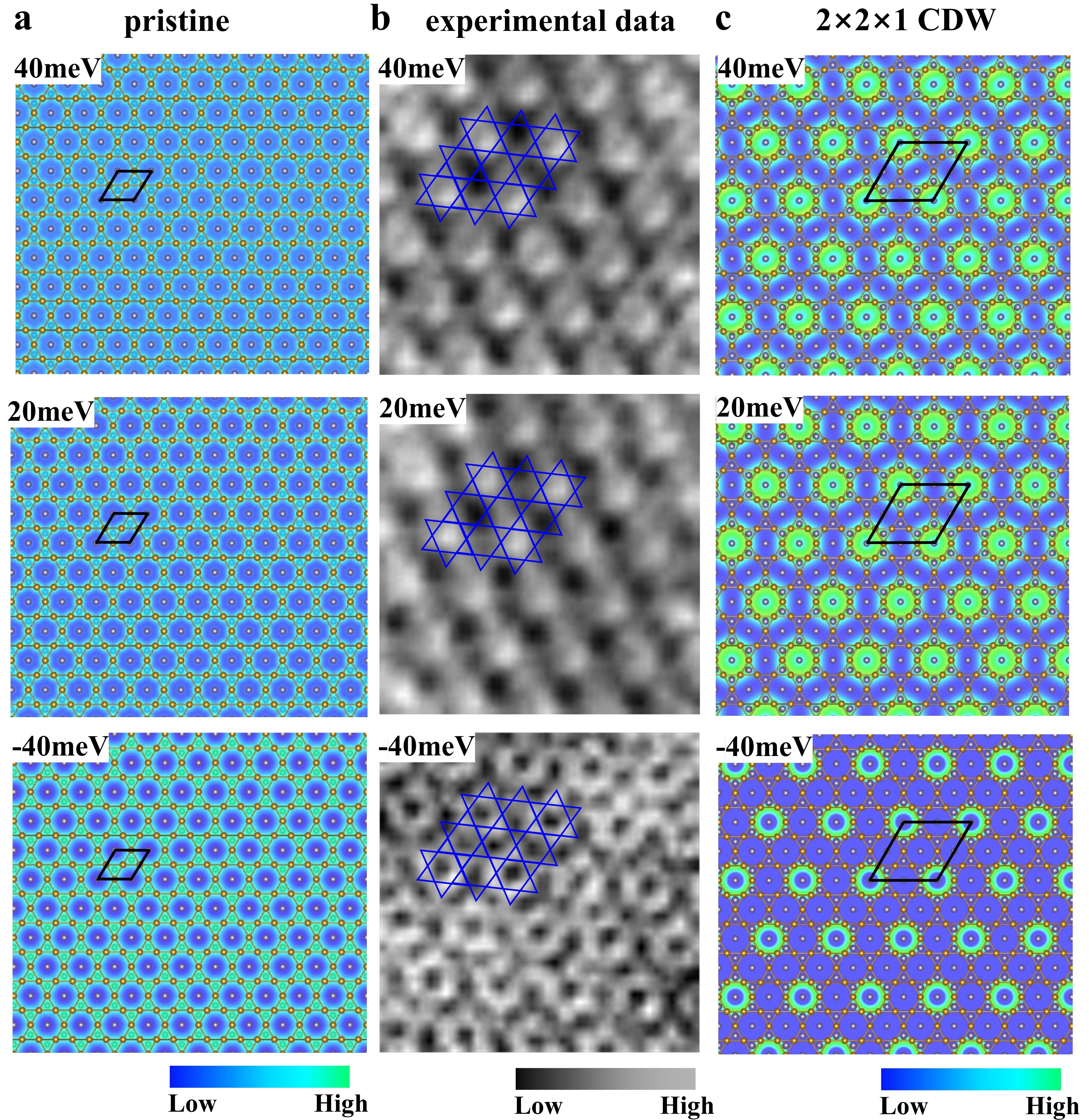
To further prove that the distorted 221 CDW phase correctly captures the experimentally observed CDW ground state, we show our STM measurements of the density of states and compare these with our theoretical predictions. Figure 2a simulates the charge distribution of the pristine phase at the Fe kagome surface. The charge is mainly distributed on the Fe-triangles and its distribution will not change significantly as the energy moves around the Fermi level of the pristine phase. In contrast, in the 22 CDW phase, STM measurements show a clear Fermi-level-dependent charge distribution (Figure 2b). At 20 and 40meV above the Fermi energy, the charge is mainly distributed in the Fe-hexagon and its adjacent Fe-triangles, but not in its neighboring Fe-hexagons. At 40 meV below the Fermi energy, the center of the bright Fe-hexagons becomes dimmer, and the charge is mainly distributed around the boundary of the Fe-hexagons and Fe-triangles. The surface charge distribution based on the 221 CDW phase presented in Figure 2c captures the behavior seen in STM plots. These results show that our predicted 221 CDW phase correctly captures the distorted 22 charge ordering structure observed experimentally in FeGe.
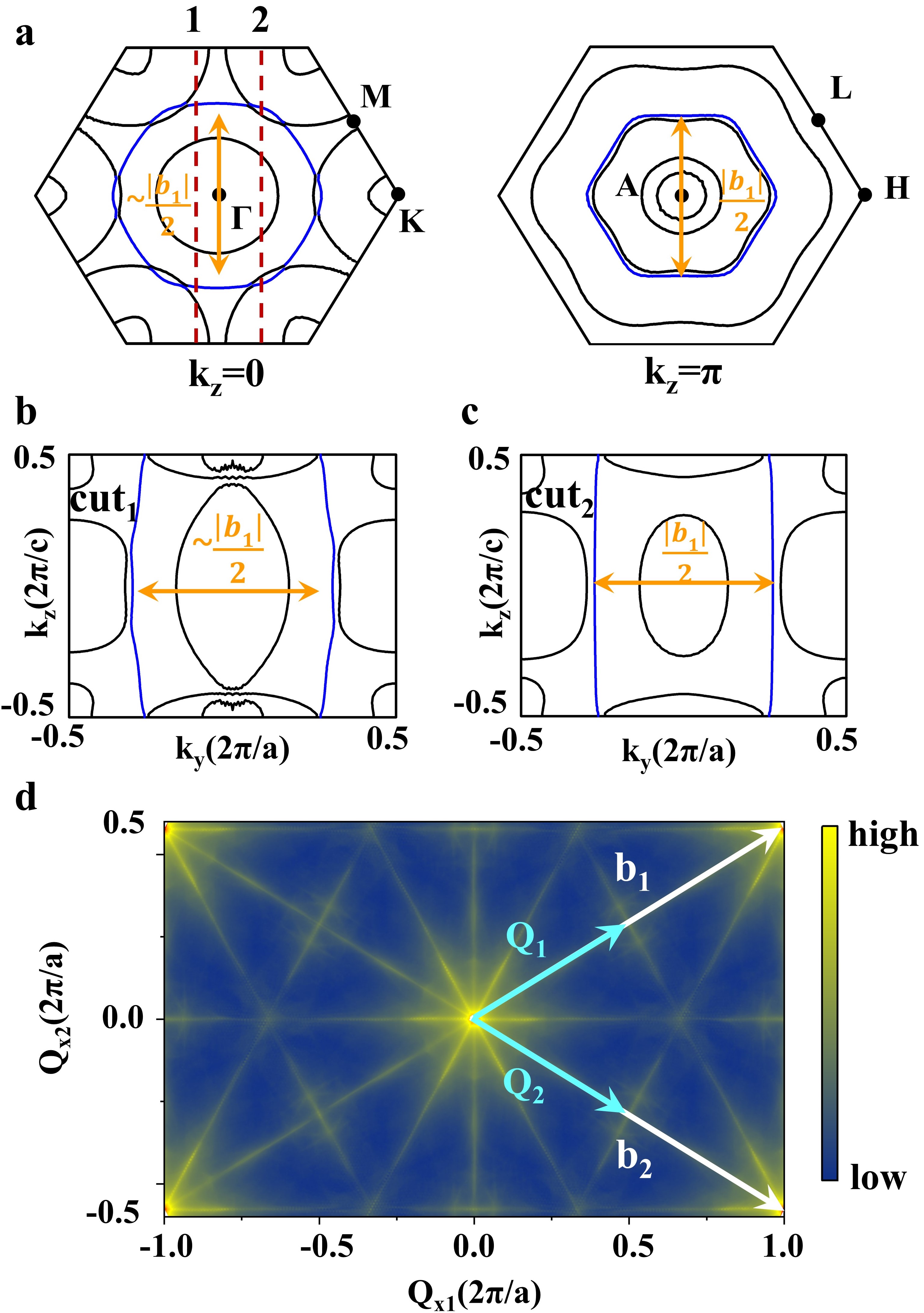
We turn now to discuss the origin of the CDW interaction that induces atomic distortions. In this connection, we first checked the Fermi surface of the pristine phase (Figure 3a-c). Interestingly we observed a very similar hexagonal Fermi surface both at =0 and = planes (colored blue in Figure 3a). This indicates that the colored states have very small dispersion along the -direction and that a hexagonal prismatic shape is present in the Fermi surface (Figure S5). The Fermi surface in the plane also shows this behavior (Figure 3b,c). The momentum separation of the quasi-one-dimensional parallel sides of the hexagonal-prism-shaped Fermi surface is about half of the unit vector of the pristine phase, as indicated by the yellow arrows in Figure 3a-c. To further demonstrate the role of Fermi-surface nesting in the CDW formation, we calculate the zero frequency susceptibility , i.e. the Lindhard response function31, 32, 33, 34, to determine the nesting vector. The two-dimensional renormalized Lindhard function is plotted in Figure 3d. Indeed the maxima are located at the center of the boundary of Brillouin zone (BZ) with the nesting vectors = (0.5, 0) and =(0, 0.5). This is in accord with the corresponding experimental observations18, 19. These results indicate that the Fermi-surface nesting is the likely driver of the 221 CDW phase. The role of electron-phonon coupling in this connection, however, deserves further attention.
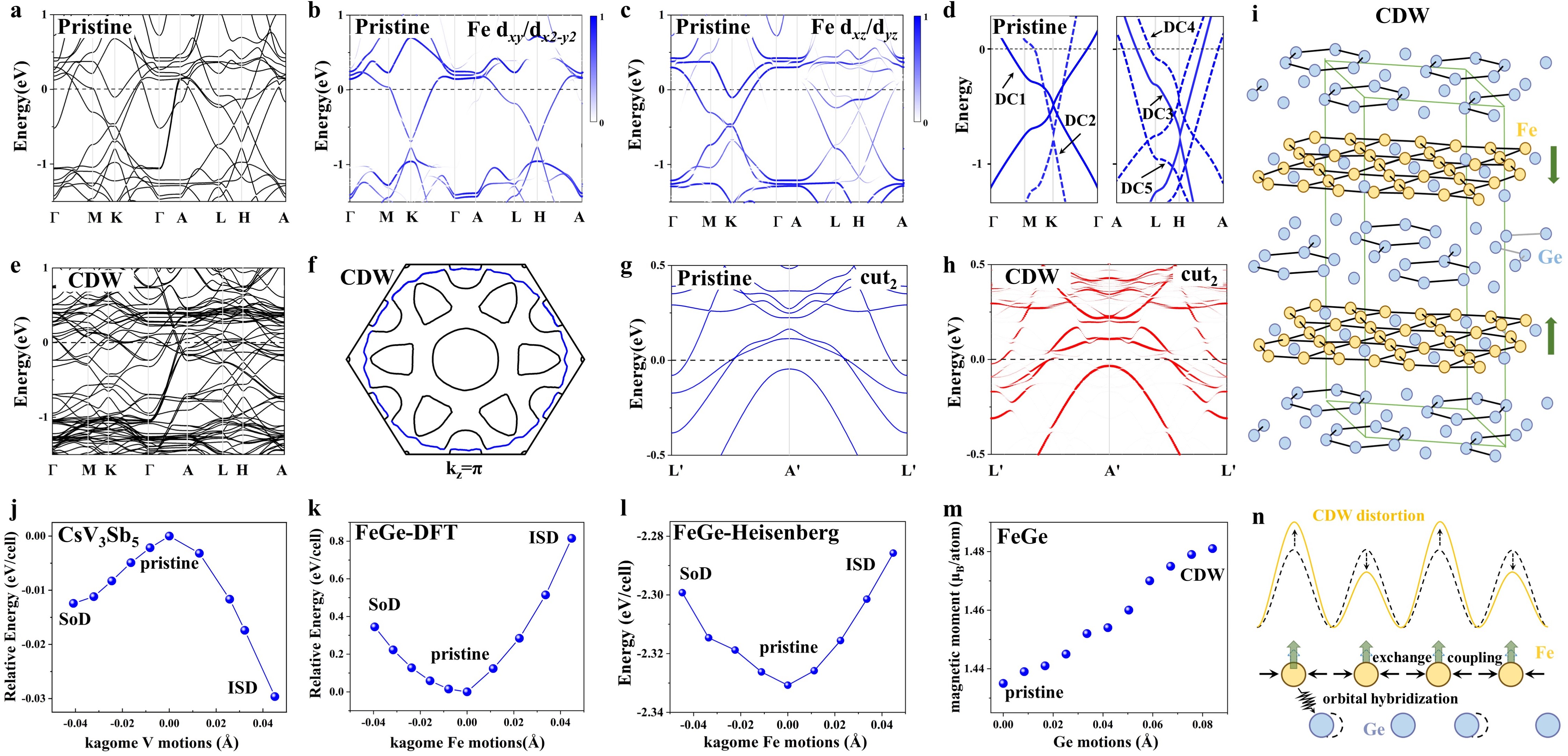
To gain further insight into the Fermi surface nesting scenario, we consider the electronic band structure of the pristine phase. Figure 4a depicts the electronic band structure of the pristine phase with SOC. The Fe- orbital-projected band structures to focus on the singularity of the kagome lattice are shown in Figure 4b,c. The ’flat bands’ are seen to lie slightly above the Fermi energy with fairly large bandwidths, which is consistent with previous studies30. We identify five Dirac cones (DCs) derived from the kagome lattice, which display van Hove singularities at the M/L points and Dirac points at the K/H points. A schematic diagram of these Dirac cones is shown in Figure 4d. Notably, DC2 and DC3 possess similar dispersions, but the related van Hove singularities lie at different energies. This is because the d orbitals, which dominate DC2 and DC3, lie in the kagome plane, and their hybridization with the upper and lower Ge atoms is weak. In contrast, the other three Dirac cones are mainly contributed by the out-of-plane dyz orbitals, and due to their strong hybridization with Ge orbitals, they show different dispersions in the =0 and = planes. The DC1 and DC3 Dirac cones shown by the solid-blue lines in Figure 4d play a major role in producing the hexagonal prism highlighted in Figure 3. The kagome-derived DC1 plays a major role in the hexagonal Fermi surface in the =0 plane, while the main contribution to the hexagonal Fermi surface gradually becomes DC3 as the 2D Fermi surface lifts from =0 to .
Now we discuss the effects of CDW interaction on the band structure. The E-k dispersion in the 221 CDW phase with the inclusion of SOC is given in Figure 4e. Most kagome features: the Dirac points and the flat bands can still be observed in the 221 CDW phase. The main effects of the CDW interactions are on states that are nested by the CDW Q-vectors. Taking the constant energy contour at kz= at 10 meV below the Fermi energy as an example, the blue hexagonal contour in the pristine phase changes into a circle-like contour in the 221 CDW phase (Figure 4f and S7). This evolution of the constant energy contours weakens Fermi surface nesting and induces CDW instability. Energy dispersion along with L′-A′-L′ in cut2 plane of the pristine phase is shown in Figure 4g, and the unfolded band structure of the 221 CDW phase along the same path is shown in Figure 4h. A clear gap-opening due to CDW interactions can be seen along this path.
We emphasize that the Fermi surface nesting comes from the kagome-derived Dirac cones, but structural distortions originate from motions of the Ge atoms, which lead to the formation of Ge bonds along the c axis and generalized kekulé distortions35, 36, 37 in the honeycomb layer: the resulting shortest bonds form an ”O”/”Y” shaped pattern as shown in Figure 4i. In the nonmagnetic kagome material AV3Sb5 (A=K, Rb, and Cs), the star of David (SoD) and the inverse star of David (ISD) distortion of the kagome layer decrease the total energy (Figure 4j). However, in FeGe, the Fermi surface nesting related to Fe atoms drives the motion of the Ge atoms instead. This unconventional distortion is caused by the intertwining of magnetism and CDW interactions. Our analysis shows that the SoD/ISD distortion in the Fe kagome layers will increase the total energy (Figure 4k). Our Heisenberg model-based calculations (Note 3 in Supporting Information) yield a similar behavior (Figure 4l). These results show that the magnetic exchange coupling tends to force the Fe atoms to remain in their original positions in the kagome layer, while the CDW interaction tends to move the Fe atoms away from their original positions. As a consequence of these two competing tendencies, the Fermi surface nesting forces are transmitted to the Ge atoms through the hybridization of Fe and Ge orbitals (Figure S10), resulting in the motion of Ge atoms in the 221 CDW phase.
In the latest experiments, the observed enhancement of the magnetic moment may be explained by the chiral flux phase of circulating currents and the effects of electronic correlations independent of Fermi surface nesting18. Our calculations show that the magnetic moment of the Fe atom in the 221 CDW phase is 1.48 , which is greater than the value of 1.44 in the pristine phase. This magnetic moment enhancement found in our work is consistent with aforementioned experimental observations. To better understand this effect, we calculated the spin-resolved partial density of states associated with Fe atoms. In the 221 CDW phase, the spin-up (spin-down) states increase (decrease) in the top kagome layers and behave in an opposite manner in the bottom Fe-kagome layer, which leads to the magnetic enhancement of Fe atoms (Figure S11). To analyze whether such an enhancement is related to Ge motions, we calculated the change of magnetic moment with the size of Ge motions. As shown in Figure 4m, the magnetic moment increases approximately linearly with Ge displacement indicating that the motions of Ge atoms can lead to greater spin splitting of Fe atoms, which, in turn, enhances the magnetic moments.
2 Conclusion
In summary, we have investigated the structural and electronic properties of antiferromagnetic kagome metal FeGe. Our in-depth analysis of the ground state 221 CDW phase indicates that this phase will transform into the pristine phase at a temperature of 80 K, which is comparable to the corresponding experimentally measured transition temperature of 100-110 K18, 19. Our predicted 221 CDW phase accurately captures the salient topographic and spectroscopic features our STM/STS experiments and the experimentally observed enhancement of the magnetic moment18, 19. Our study unveils the presence of an unconventional intertwining between magnetism and CDW interactions in kagome magnets (Figure 4n), which forces Fe atoms of the kagome layers to remain at the original positions, but leads to the motion of Ge atoms and the formation of a generalized kekulé distortion in the Ge honeycomb layers. Since Kekulé distortions in graphene open conduction channels between the valleys that influence optical absorption and conductivity37, we expect the generalized kekulé distortions in FeGe to also yield interesting physical effects. Our study provides insight into the CDW phase and indicates that further exploration of the topological nature of the ground state of magnetic kagome-honeycomb lattices and their transport and optical responses will be interesting. We also identify the structure of the 222 CDW phase and the structures of the two related metastable 11 and 221 phases (Table S1), which could provide theoretical support for future experiments.
3 Methods
The CDW phases are proposed based on the structure search method implemented in the CALYPSO 20, 21, 22 code. First, we fix the positions of the Ge atoms in the volume of the 221 pristine phase and generate positions of the Fe atoms randomly. Then, we fix the positions of the Fe atoms and generate the positions of Ge atoms randomly. After generating such 221 structures, we relax them using first-principles calculations using the Vienna ab-initio Simulation Package (VASP)38 within the Perdew-Burke-Ernzerhof exchange-correlation functional39. The projector augmented-wave method 40 is implemented with 34 and 44 treated as valence electrons for Fe and Ge atoms, respectively. The cut-off energy of 520 eV and a dense k-point sampling of the Brillouin zone with a spacing of 2 0.03 Å-1 are used to ensure the convergence of enthalpy within 1 meV/atom. The phonon spectra are calculated with the frozen phonon method and the Gibbs free energy is simulated in the framework of quasi-harmonic approximation as employed in PHONOPY 41 code. The post-processing of band and DOS calculations is performed by the VASPKIT tool 42. The pristine phase of FeGe is found to be dynamically stable at 0 K, indicating that the CDW transition is induced by electrons nested at the Fermi level. Therefore, we focus on the electronic contribution to the CDW instability and interpret our results using a simple picture of the Fermi-surface nesting vectors. We also carry out an accurate calculation of the electronic susceptibility with =0 Lindhard response function. In the constant-matrix-element approximation,43, 34 0(q,0) is given by:
0(q,0) =
Here, the sum is over the whole first Brillouin zone. The Fermi-Dirac distribution is: fK= The STM images of the 221 CDW and the pristine phases are simulated using a slab model, which has been used previously to simulate STM images in AV3Sb5 (A=K, Rb, Cs) 11. The STM images for the Fe kagome surface of pristine and 221 CDW phases are simulated using a 3-unit-cell thick slab (144 atoms) with a vacuum layer of 10 Å. The STM images are calculated with a fixed height of 3 Å above the surface in the energy range of ± 25 meV relative to the given energy. Structural relaxation and SOC effect are not considered in the STM simulations.
4 Author Contributions
S. S., J.-X. Y., I. B., and J.-Y. Y. contributed equally to this work. G.C. was responsible for the overall research direction, planning, and integration among different research units. All authors contributed to the intellectual content and the writing of this work.
5 Acknowledgment
The work was supported by the National Research Foundation, Singapore under its Fellowship Award (NRF-NRFF13-2021-0010) and the Nanyang Technological University start-up grant (NTUSUG). Work at Princeton University was supported by the Gordon and Betty Moore Foundation (GBMF4547 and GBMF9461; M.Z.H.). J.Y.Y. and Y.P.F. are supported by the Ministry of Education, Singapore, under its MOE AcRF Tier 3 Award MOE2018-T3-1-002. The work at Northeastern University was supported by the US Department of Energy (DOE), Office of Science, Basic Energy Sciences Grant No. DE-SC0022216 and benefited from Northeastern University’s Advanced Scientific Computation Center and the Discovery Cluster, and the National Energy Research Scientific Computing Center through DOE Grant No. DE-AC02-05CH11231.
Detailed structure information, structures, electronic properties, and Heisenberg models of antiferromagnetic kagome FeGe.
References
- 1 Hou, C. Y.; Chamon, C.; Mudry, C. Electron fractionalization in two-dimensional graphenelike structures. Phys. Rev. Lett. 2007, 98, 186809.
- 2 Gutiérrez, C.; Kim, C. J.; Brown, L.; Schiros, T.; Nordlund, D.; Lochocki, E. B.; Shen, K. M.; Park, J.; Pasupathy, A. N. Imaging chiral symmetry breaking from kekulé bond order in graphene. Nat. Phys. 2016, 12, 950.
- 3 Bao, C. H.; Zhang, H. Y.; Zhang, T.; Wu, X.; Luo, L. P.; Zhou, S. H.; Li, Q.; Hou, Y. H.; Yao, W.; Liu, L. W.; Yu, P.; Li, J.; Duan, W. H.; Yao, H.; Wang, Y. L.; Zhou, S. Y. Experimental evidence of chiral symmetry breaking in kekulé-ordered graphene. Phys. Rev. Lett. 2021, 126, 206804.
- 4 Hasan, M. Z.; Chang, G. Q.; Belopolski, I.; Bian, G.; Xu, S.-Y.; Yin J.-X. Weyl, Dirac and high-fold chiral fermions in topological quantum matter. Nat. Rev. Mater. 2021, 6, 784.
- 5 Yin, J.-X.; Lian, B.; Hasan, M. Z. Topological kagome magnets and superconductors. Nature 2022, 612, 647.
- 6 Chen, H.; Yang, H. T.; Hu, B.; Zhao, Z.; Yuan, J.; Xing, Y. Q.; Qian, G. J.; Huang, Z. H.; Li, G.; Ye, Y. H.; Ma, S.; Ni, S. L.; Zhang, H.; Yin, Q. W.; Gong, C. S.; Tu, Z. J.; Lei, H. C.; Tan, H. X.; Zhou S.; Shen, C. M.; Dong, X. L.; Yan, B. H.; Wang Z. Q.; Gao H. J. Roton pair density wave in a strong-coupling kagome superconductor. Nature 2021, 599, 222.
- 7 Zhao, H.; Li, H.; Ortiz, B. R.; Teicher, S. M.; Park, T.; Ye, M. X.; Wang, Z. Q.; Balents, L.; Wilson S. D.; Zeljkovic, I. Cascade of correlated electron states in the kagome superconductor CsV3Sb5. Nature 2021, 599, 216.
- 8 Nie, L. P.; Sun, K. L.; Ma, W. R.; Song, D. W.; Zheng, L. X.; Liang, Z. W.; Wu, P.; Yu, F. H.; Li, J.; Shan, M.; Zhao, D.; Li, S. J.; Kang, B. L.; Wu, Z. M.; Zhou, Y. B.; Liu, K.; Xiang, Z. J.; Ying, J. J.; Wang, Z. Y.; Wu, T.; Chen, X. H. Charge-density-wave-driven electronic nematicity in a kagome superconductor. Nature 2022, 604, 59.
- 9 Jiang,Y. X.; Yin, J.-X.; Denner, M. M.; Shumiya, N.; Ortiz, B. R.; Xu, G.; Guguchia, Z.; He, J. Y.; Hossain, M. S.; Liu, X. X.; Ruff, J.; Kautzsch, L.; Zhang, S. S.; Chang, G. Q.; Belopolski, I.; Zhang, Q.; Cochran, T. A.; Multer, D.; Litskevich, M.; Cheng, Z.-J.; Yang, X. P.; Wang, Z. Q.; Thomale, R.; Neupert, T.; Wilson S. D.; Hasan, M. Z. Unconventional chiral charge order in kagome superconductor KV3Sb5. Nat. Mater. 2021, 20, 1353.
- 10 Li, H. X.; Zhang, T. T.; Yilmaz, T.; Pai, Y. Y. ; Marvinney, C. E.; Said, A.; Yin, Q. W.; Gong, C. S.; Tu, Z. J.; Vescovo, E. ; Nelson, C. S.; Moore, R. G.; Murakami, S.; Lei, H. C.; Lee, H. N.; Lawrie, B. J.; Miao, H. Observation of unconventional charge density wave without acoustic phonon anomaly in kagome superconductors AV3Sb5(A=Rb, Cs). Phys. Rev. X 2021, 11, 031050.
- 11 Tan, H. X.; Liu, Y. Z.; Wang, Z. Q.; Yan, B. H. Charge density waves and electronic properties of superconducting kagome metals. Phys. Rev. Lett. 2021, 127, 046401.
- 12 Neupert, T.; Denner, M. M.; Yin, J. X.; Thomale, R.; Hasan, M. Z. Charge order and superconductivity in kagome materials. Nat. Phys. 2022, 18, 137.
- 13 Yu, F. H.; Ma, D. H.; Zhuo, W. Z.; Liu, S. Q.; Wen, X. K.; Lei, B.; Ying J. J.; Chen,X. H. Unusual competition of superconductivity and charge-density-wave state in a compressed topological kagome metal. Nat. Commun. 2021, 12, 3645.
- 14 Mielke, C. III; Das, D.; Yin, J.-X.; Liu, H.; Gupta, R.; Jiang, Y.-X.; Medarde, M.; Wu, X.; Lei, H. C.; Chang, J.; Dai, P. C.; Si, Q.; Miao, H.; Thomale, R.; Neupert, T.; Shi, Y.; Khasanov, R.; Hasan, M. Z.; Luetkens, H.; Guguchia, Z. Time-reversal symmetry-breaking charge order in a kagome superconductor. Nature 2022, 602 245.
- 15 Yang, H. J.; Kim, H. S.; Jeong, M. Y.; Kim, Y. B.; Han, M. J.; Lee, S. Intertwining orbital current order and superconductivity in kagome metal. 2022, arXiv:2203.07365, arXiv. DOI: 10.48550/arXiv.2203.07365 (accessed May 21, 2022).
- 16 Mielke, C. III; Qin, Y.; Yin, J.-X.; Nakamura, H.; Das, D.; Guo, K.; Khasanov, R.; Chang, J.; Wang, Z. Q.; Jia, S.; Nakatsuji, S.; Amato, A.; Luetkens, H.; Xu, G.; Hasan, M. Z.; Guguchia, Z. Nodeless kagome superconductivity in LaRu3Si2. Phys. Rev. Materials 2021, 5, 034803.
- 17 Jiang, Y.-X.; Yin, J.-X.; Denner, M. M.; Shumiya, N.; Ortiz, B. R.; Xu, G.; Guguchia, Z.; He, J. Y.; Hossain, M. S.; Liu, X. X.; Ruff, J.; Kautzsch, L.; Zhang, S. S.; Chang, G. Q.; Belopolski, I.; Zhang, Q.; Cochran, T. A.; Multer, D.; Litskevich, M.; Cheng, Z. J.; Yang, X. P.; Wang, Z. Q.; Thomale, R.; Neupert, T.; Wilson, S. D.; Hasan,M. Z. Unconventional chiral charge order in kagome superconductor KV3Sb5. Nat. Mater. 2021, 20, 1353.
- 18 Teng, X. K.; Chen, L. B.; Ye, F.; Rosenberg, E.; Liu, Z. Y.; Yin, J.-X.; Jiang, Y.-X.; Oh, J. S.; Hasan, M. Z.; Neubauer, K. J.; Gao, B.; Xie, Y. F.; Hashimoto, M.; Lu, D. H.; Jozwiak, C.; Bostwick, A.; Rotenberg, E.; Birgeneau, R. J.; Chu, J. H.; Yi, M.; Dai, P. C. Discovery of charge density wave in a kagome lattice antiferromagnet. Nature 2022, 609, 490.
- 19 Yin, J.-X.; Jiang, Y,-X,; Teng, X. K.; Hossain, M. S.; Mardanya, S.; Chang, T.-R.; Ye, Z. J.; Xu, G.; Denner, M. M.; Neupert, T.; Lienhard, B.; Deng, H.-B.; Setty, C.; Si, Q. M.; Chang, G. Q.; Guguchia, Z.; Gao, B.; Shumiya, N.; Zhang, Q.; Cochran, T. A.; Multer, D.; Yi, M.; Dai, P. C.; Hasan, M. Z. Discovery of charge order and corresponding edge state in kagome magnet FeGe. Phys. Rev. Lett. 2022, 129, 166401.
- 20 Wang, Y. W.; Lv, J.; Zhu, L.; Ma, Y. M. Crystal structure prediction via particle-swarm optimization. Phys. Rev. B 82, 094116 (2010).
- 21 Wang, Y. W.; Lv, J.; Zhu, L.; Ma, Y. M. CALYPSO: a method for crystal structure prediction. Comput. Phys. Commun. 2012, 183, 2063.
- 22 Gao, B.; Gao, P. Y.; Lu, S. H.; Lv, J.; Wang, Y. C.; Ma. Y. M. Interface structure prediction via CALYPSO method. Sci. Bull. 2019, 64, 301.
- 23 Henkelman, G.; Uberuaga, B. P.; Jónsson, H. A climbing image nudged elastic band method for finding saddle points and minimum energy paths. J Chem. Phys. 2000, 113, 9901.
- 24 Mills, G.; Jónsson, H.; Schenter, G. K. Reversible work transition state theory: application to dissociative adsorption of hydrogen. Surf. Sci. 1995, 324, 305.
- 25 Sheppard, D.; Terrell, R.; Henkelman, G. Optimization methods for finding minimum energy paths. J Chem. Phys. 2008, 128, 134106.
- 26 Weber, F.; Rosenkranz, S.; Castellan, J.-P.; Osborn, R.; Hott, R.; Heid, R.; Bohnen, K.-P.; Egami, T.; Said, A. H.; Reznik, D. Extended phonon collapse and the origin of the charge-density wave in 2H-NbSe2. Phys. Rev. Lett. 2011, 107, 107403.
- 27 Diego, J.; Said, A. H.; Mahatha, S. K.; Bianco, R,; Monacelli, L.; Calandra, M.; Mauri, F.; Rossnagel, K.; Errea, I.; Blanco-Canosa, S. Van der Waals driven anharmonic melting of the 3D charge density wave in VSe2. Nat. Commun. 2021, 12, 598.
- 28 Kvashnin, Y.; VanGennep, D.; Mito, M.; Medvedev, S. A.; Thiyagarajan, R.; Karis, O.; Vasiliev, A. N.; Eriksson, O.; Abdel-Hafiez, M. Coexistence of superconductivity and charge density waves in tantalum disulfide: experiment and theory. Phys. Rev. Lett. 2020, 125, 186401.
- 29 Xi, X. X.; Zhao, L.; Wang, Z. F.; Berger, H.; Forró, L.; Shan, J.; Mak, K. F. Strongly enhanced charge-density-wave order in monolayer NbSe2. Nat. Nanotechnol. 2015, 10, 765.
- 30 Setty, C.; Lane, C. A.; Chen, L.; Hu, H. Y.; Zhu, J.-X.; Si, Q. M. Electron correlations and charge density wave in the topological kagome metal FeGe. 2022, arXiv:2203.01930, arXiv. DOI: 10.48550/arXiv.2203.01930 (accessed Apr 6, 2022).
- 31 Lindhard, J. On the properties of a gas of charged particles. Dan. Vid. Selsk Mat.-Fys. Medd. 1954, 28, 8.
- 32 Borisenko, S. V.; Kordyuk, A. A.; Yaresko, A. N.; Zabolotnyy, V. B.; Inosov, D. S.; Schuster, R.; Büchner, B.; Weber, R.; Follath, R.; Patthey, L.; Berger, H. Pseudogap and charge density waves in two dimensions. Phys. Rev. Lett. 2008, 100, 196402.
- 33 Borisenko, S. V.; Kordyuk, A. A.; Zabolotnyy, V. B.; Inosov, D. S.; Evtushinsky, D.; Büchner, B.; Yaresko, A. N.; Varykhalov, A.; Follath, R.; Eberhardt, W.; Patthey, L.; Berger, H. Two energy gaps and fermi-surface “arcs” in NbSe2. Phys. Rev. Lett. 2009, 102, 166402.
- 34 Dugdale, S. B. Life on the edge: a beginner’s guide to the Fermi surface. Phys. Scr. 2016, 91, 053009.
- 35 Kekulé, A. Studies on aromatic compounds. Ann. Chem. Pharm. 1865, 137, 129.
- 36 Chamon, C. Solitons in carbon nanotubes. Phys. Rev. B 2000, 62, 2806.
- 37 Herrera, S. A.; Naumis, G. G. Electronic and optical conductivity of kekulé-patterned graphene: intravalley and intervalley transport. Phys. Rev. B 2020, 101, 205413.
- 38 Kresse, G.; Furthmüller, J. Efficient iterative schemes for ab initio total-energy calculations using a plane-wave basis set. Phys. Rev. B 1996, 54, 11169.
- 39 Perdew, J. P.; Burke, K.; Ernzerhof, M. Generalized gradient approximation made simple. Phys. Rev. Lett. 1996, 77, 3865.
- 40 Blöchl, P. E. Projector augmented-wave method. Phys. Rev. B 1994, 50, 17953.
- 41 Togo, A.; Oba, F.; Tanaka, I. First-principles calculations of the ferroelastic transition between rutile-type and CaCl2-type SiO2 at high pressures. Phys. Rev. B 2008, 78, 134106.
- 42 Wang, V.; Xu, N.; Liu, J.-C.; Tang, G.; Geng, W.-T. VASPKIT: a user-friendly interface facilitating high-throughput computing and analysis using VASP code. Comput. Phys. Commun. 2021, 267, 108033.
- 43 Zhu, X. T.; Cao, Y. W.; Zhang, J. D.; Plummer, E. W.; Guo, J. D. Classification of charge density waves based on their nature. Proc. Natl. Acad. Sci. U. S. A. 2015, 112, 2367.