Emergence of Interlayer Coherence in Twist-Controlled Graphene Double Layers
Abstract
We report enhanced interlayer tunneling with reduced linewidth at zero interlayer bias in a twist-controlled double monolayer graphene heterostructure in the quantum Hall regime, when the top () and bottom () layer filling factors are near and , and the total filling factor or . The zero-bias interlayer conductance peaks are stable against variations of layer filling factor, and signal the emergence of interlayer phase coherence. Our results highlight twist control as a key attribute in revealing interlayer coherence using tunneling.
In closely spaced double layer systems placed in the quantum Hall regime, the interlayer and intralayer interactions lead to ground states not present in single layers, including even denominator fractional quantum Hall states (QHSs) at total Landau level (LL) filling and [1, 2, 3, 4], as well as states that are interlayer electron-hole pair condensates [5] with enhanced interlayer coherence. Experimental evidence for this phenomenon in GaAs double layers includes Josephson-like interlayer tunneling [6, 7, 8], counterflow with near zero dissipation [9, 10, 11, 12], and Andreev reflection [13]. In graphene double layers, quantized Hall drag [14] and counterflow [15] measurements have provided evidence of particle-hole pairing at total filling factor and . Here, we investigate interlayer tunneling in a twist-controlled double monolayer graphene heterostructure, where tunneling in the quantum Hall effect regime provides insight into interlayer phase coherence. We observe enhanced interlayer tunneling at zero interlayer bias at and that is immune to changes in individual layer filling factors, a fingerprint of nascent interlayer phase coherence.
Figure 1(a) shows a schematic of the twist-controlled double monolayer graphene-hBN heterostructure, which consists of two rotationally aligned and independently contacted graphene monolayers separated by a nm thick hBN tunnel barrier. Top and bottom hBN dielectrics encapsulate the heterostructure [16], and top () and bottom () graphite gate biases tune the layers densities. The crystal axis alignment of the two graphene layers [17] establishes energy and momentum conserving interlayer tunneling [18, 19, 20, 21], which leads to interlayer voltage-current characteristics with gate tunable negative differential resistance (NDR), and provides sensitivity to interlayer phase coherence. Multiple contacts to each graphene layer allow four-point interlayer current () vs. interlayer voltage () measurements to decouple interlayer tunneling characteristics from contact resistances. Figure 1(b) shows an optical micrograph of the heterostructure.
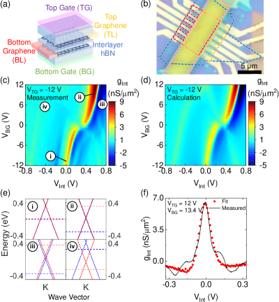
Figure 1(c) shows the interlayer conductance vs. and , measured at a top gate bias of V, temperature K; is applied on the top layer, while the the bottom layer is held at ground. The data show resonant tunneling manifested by a peak and NDR, which evolve with and , and correspond to the biasing condition where the layers energy bands are aligned, indicating energy and momentum conserving tunneling. We can explain the interlayer tunneling characteristics using a single-particle model [21, 22],
| (1) |
where is the energy, () is the state occupancy in the top (bottom) layer, and the elementary charge. The tunneling rate [] is given by
| (2) |
where is the interlayer coupling, and the spectral density in the top and bottom layers is assumed to be Lorentzian,
| (3) |
where is the top, bottom graphene energy-momentum dispersion, respectively, and the quasiparticle state energy broadening, assumed to be the same in both layers. The top (bottom) graphene layer density () is calculated using the following set of equations:
| (4) | |||||
| (5) | |||||
where () is the top (bottom) gate capacitance, the interlayer capacitance, () is the top (bottom) layer chemical potential referenced to charge neutrality.
Figure 1(d) shows calculated for the biasing conditions of Fig. 1(c). An interlayer coupling of eV best fits the measurements. Figure 1(e) shows the calculated bands of the top and bottom graphene layers corresponding to the regimes labeled in Fig. 1(c). At points (i) and (ii) a peak in interlayer conductance occurs because the energy bands are aligned. At points (iii) and (iv) the bands are energetically misaligned, suppressing the interlayer tunneling. Figure 1(f) shows vs. measured at and values with the resonant peak at V. A fit of the experimental data yields meV. The values increase slightly with the layer density (see Fig. S1 of Supplemental Material). To assess the rotational alignment between the two layers, we performed calculations similar to Fig. 1(d) data, but including a twist between the two layers. A comparison with experimental data indicate the alignment is within (see Fig. S2 and Fig. S3 of Supplemental Material).
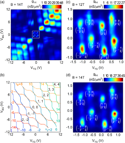
In a perpendicular magnetic field () the electrons occupy LLs, with a fourfold, spin and valley degeneracy in the absence of interactions [23, 24]. In Fig. 2(a), we plot measured at V as a function of and at T, and K (see Supplemental Material Fig. S4 for data measured at T). The data show oscillations vs. and , associated with LLs in both layers. To understand Fig. 2(a) data, we employ Eqs. (4–5) and , where is the highest occupied orbital LL index. Figure 2(b) shows the LL filling factor () in the top (bottom) layer, and the top (bottom) layer orbital LL indices ) along the diagonal. We determine nF/cm2, nF/cm2, and F/cm2. The model accurately captures the experimental oscillations, with minima at , consistent with a single-particle picture where minima (maxima) occur under full (partial) orbital LL fillings due to the availability of extended states.
In Figs. 2(c) and 2(d), we highlight as a function of and with and K, inside the sector for and T respectively. Along the diagonal we observe clear maxima at and , where both the top and bottom filling factors and are equal half-integers. The states ( correspond to a total filling factor of , and ( correspond to . In addition, we observe maxima at ( and , corresponding to the imbalanced state at . No peaks are observed at or . Figures 2(c) and 2(d) data depart markedly from observations made in LLs, where no peaks are observed when the layers are at half LL filling factors.
A mechanism that leads to enhanced values is the formation of interlayer phase coherent QHSs. Indeed, at T the effective layer separation is sufficiently small that inter- and intralayer interaction become comparable; is the magnetic length. These conditions are expected to lead to phase coherence between electrons in different layers, which manifests in the case of short range order [25, 26, 27] as an enhanced Josephson-like interlayer tunneling [6, 7, 8].
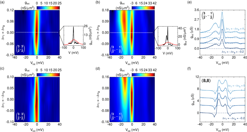
To shed light on the mechanisms leading to enhanced tunneling at many half-integer layer fillings in Fig. 3(a) we plot vs. , when we concomitantly vary and by equal amounts away from . The inset shows vs. when (black), and vs. interlayer electrostatic potential difference at T (red), illustrating a much sharper zero-bias peak at T compared to the T data. A similar dataset measured for is shown in Fig. 3(b). Figures 3(c) and 3(d) show vs. and corresponding to and , respectively. Interestingly, for both and , corresponding to and , peaks are observed at with widths significantly smaller compared to the T resonances [see e.g. Fig. 1(f)]. The peak positions are stable at V, and do not respond to layer filling factor variations. In contrast, the conductance in a noninteracting electron picture is proportional to an integral over energy of the layers density-of-states (DOS) product evaluated at in one layer and in the other layer. This picture predicts zero-bias peaks only when the DOS is maximized at the Fermi level in both layers, a property that cannot be maintained over finite ranges of layer filling factors. Indeed, calculations of vs. and using a single-particle interlayer tunneling model for half-filled Landau levels (see Supplemental Material Fig. S5) show a peak that evolves with , in clear contrast to Fig. 3(a)–3(d) data.
The zero-bias peaks demonstrate the emergence of phase coherence between the two graphene monolayers at and , where electrons occupy a coherent superposition of states in both layers. We contrast the zero-bias peaks observed at and with measurements at in the half-filled sector. Figures 3(e) and 3(f) compare vs. and for and respectively. For the case we observe minima at , as a opposed to a peak, consistent with a tunneling gap at the Fermi level, similar to the suppression of tunneling between two half-filled uncorrelated LLs [28, 29]. We observe similar minima at at other half-filled LLs outside the sector, suggesting that interlayer phase coherence is present at and , but not elsewhere.
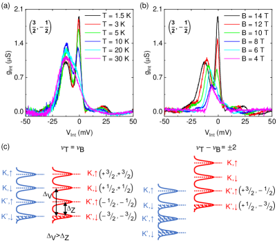
The temperature dependence of the vs. zero-bias peak present at is shown in Fig. 4(a). The zero-bias peak for decreases as is increased. A similar decrease in peak height as temperature is increased is observed at other and states (see Supplemental Material Fig. S6). At K, the interlayer conductance at with the background tunneling removed () vanishes, signaling the interlayer phase coherence is no longer present. The dependence of is particularly interesting for , since the height of the zero-bias peak drops sharply with increasing temperature. In contrast, the side-peak at remains present and broadens noticeably with increasing temperature, which suggests the zero-bias peak is driven by interlayer phase coherence in the many-body ground state, whereas the side-peak is not. Figure 4(b) shows the dependence of the vs. at . Reducing from T to T corresponds to varying from to , which renders the double layer more interacting. However, the zero-bias peak for decreases as is decreased, and is extinguished at T, likely because of static disorder.
Order in the interlayer electron-hole pair amplitude can be viewed as layer pseudospin () ferromagnetism with order in the plane. The layers’ chemical potential difference is then , where is the pseudospin component along the axis. According to the layer ferromagnet Landau-Lifshitz equations, it follows that nonequilibrium steady states with a fixed bias voltage are unstable to states with oscillatory collective dynamics. The enhanced tunneling seen experimentally in semiconductor quantum wells [6, 7, 8] have been consistently interpreted as evidence for states with nascent order that has finite temporal and/or spatial range [25, 26, 27]. The conductance due to enhanced short-range interlayer coherence is always peaked at zero bias, in contrast to single-particle resonant conductance peaks.
Because interlayer coherence is observed for and , two types of paired states can be pictured [Fig. 4(c)]. We assume that valley and spin degeneracy in the LL is lifted such that the valley splitting () dominates over the Zeeman effect () leading to a valley polarized QHS in each layer [30]. The observation of interlayer coherence at both and is consistent with spin conservation in interlayer tunnneling. The absence of tunneling at is expected since single-particle spin-flip tunneling is expected to be extremely weak in graphene, and does imply that interlayer coherence is absent in these cases. If valley is also conserved in tunneling, the observation of interlayer coherence at implies that the valley splitting in the LL does not lead to and states associated with the two sublattices of monolayer graphene, but rather a valley superposition [31, 32].
Josephson-like interlayer tunneling associated with coherence in interacting double layers require single-particle tunneling because the critical current [25, 27]. In twist-misaligned double layers single particle tunneling is suppressed because of the momentum mismatch between the band minima. The twist-aligned graphene double layer sample design ensures that single particle tunneling is not suppressed, and establishes twist control as key to probing interlayer coherence by identifying tunneling anomalies in double layers of two-dimensional materials.
Acknowledgements.
We thank Timo Hyart for useful discussions. The work at The University of Texas was supported by the National Science Foundation Grants No. EECS-2122476 and No. DMR-1720595, Army Research Office under Grant No. W911NF-17-1-0312. Work was partly done at the Texas Nanofabrication Facility supported by NSF Grant No. NNCI-1542159 and at the Texas Advanced Computing Center (TACC) at The University of Texas at Austin. K.W. and T.T. acknowledge support from the Elemental Strategy Initiative conducted by the MEXT, Japan (Grant No. JPMXP0112101001) and JSPS KAKENHI (Grant Nos. JP19H05790 and No. JP20H00354). K.U. acknowledges support from the JSPS KAKENHI Grants No. JP25107004, No. JP18H01822, No. JP21K04826, and No. JP22H05445.References
- Suen et al. [1992] Y. W. Suen, L. W. Engel, M. B. Santos, M. Shayegan, and D. C. Tsui, Phys. Rev. Lett. 68, 1379 (1992).
- Eisenstein et al. [1992a] J. P. Eisenstein, G. S. Boebinger, L. N. Pfeiffer, K. W. West, and S. He, Phys. Rev. Lett. 68, 1383 (1992a).
- Luhman et al. [2008] D. R. Luhman, W. Pan, D. C. Tsui, L. N. Pfeiffer, K. W. Baldwin, and K. W. West, Phys. Rev. Lett. 101, 266804 (2008).
- Shabani et al. [2009] J. Shabani, T. Gokmen, Y. T. Chiu, and M. Shayegan, Phys. Rev. Lett. 103, 256802 (2009).
- Eisenstein [2014] J. Eisenstein, Annual Review of Condensed Matter Physics 5, 159 (2014).
- Spielman et al. [2000] I. B. Spielman, J. P. Eisenstein, L. N. Pfeiffer, and K. W. West, Phys. Rev. Lett. 84, 5808 (2000).
- Tiemann et al. [2009] L. Tiemann, Y. Yoon, W. Dietsche, K. von Klitzing, and W. Wegscheider, Phys. Rev. B 80, 165120 (2009).
- Nandi et al. [2013] D. Nandi, T. Khaire, A. D. K. Finck, J. P. Eisenstein, L. N. Pfeiffer, and K. W. West, Phys. Rev. B 88, 165308 (2013).
- Kellogg et al. [2004] M. Kellogg, J. P. Eisenstein, L. N. Pfeiffer, and K. W. West, Phys. Rev. Lett. 93, 036801 (2004).
- Tutuc et al. [2004] E. Tutuc, M. Shayegan, and D. A. Huse, Phys. Rev. Lett. 93, 036802 (2004).
- Wiersma et al. [2004] R. D. Wiersma, J. G. S. Lok, S. Kraus, W. Dietsche, K. von Klitzing, D. Schuh, M. Bichler, H.-P. Tranitz, and W. Wegscheider, Phys. Rev. Lett. 93, 266805 (2004).
- Nandi et al. [2012] D. Nandi, A. D. K. Finck, J. P. Eisenstein, L. N. Pfeiffer, and K. W. West, Nature 488, 481 (2012).
- Finck et al. [2011] A. D. K. Finck, J. P. Eisenstein, L. N. Pfeiffer, and K. W. West, Phys. Rev. Lett. 106, 236807 (2011).
- Liu et al. [2017] X. Liu, K. Watanabe, T. Taniguchi, B. I. Halperin, and P. Kim, Nature Phys 13, 746 (2017).
- Li et al. [2017] J. I. A. Li, T. Taniguchi, K. Watanabe, J. Hone, and C. R. Dean, Nature Phys 13, 751 (2017).
- Dean et al. [2010] C. R. Dean, A. F. Young, I. Meric, C. Lee, L. Wang, S. Sorgenfrei, K. Watanabe, T. Taniguchi, P. Kim, K. L. Shepard, and J. Hone, Nature Nanotech 5, 722 (2010).
- Kim et al. [2016] K. Kim, M. Yankowitz, B. Fallahazad, S. Kang, H. C. P. Movva, S. Huang, S. Larentis, C. M. Corbet, T. Taniguchi, K. Watanabe, S. K. Banerjee, B. J. LeRoy, and E. Tutuc, Nano Letters 16, 1989 (2016).
- Britnell et al. [2013] L. Britnell, R. V. Gorbachev, A. K. Geim, L. A. Ponomarenko, A. Mishchenko, M. T. Greenaway, T. M. Fromhold, K. S. Novoselov, and L. Eaves, Nat Commun 4, 1794 (2013).
- Mishchenko et al. [2014] A. Mishchenko, J. S. Tu, Y. Cao, R. V. Gorbachev, J. R. Wallbank, M. T. Greenaway, V. E. Morozov, S. V. Morozov, M. J. Zhu, S. L. Wong, F. Withers, C. R. Woods, Y.-J. Kim, K. Watanabe, T. Taniguchi, E. E. Vdovin, O. Makarovsky, T. M. Fromhold, V. I. Falko, A. K. Geim, L. Eaves, and K. S. Novoselov, Nature Nanotech 9, 808 (2014).
- Fallahazad et al. [2015] B. Fallahazad, K. Lee, S. Kang, J. Xue, S. Larentis, C. Corbet, K. Kim, H. C. P. Movva, T. Taniguchi, K. Watanabe, L. F. Register, S. K. Banerjee, and E. Tutuc, Nano Letters 15, 428 (2015).
- Burg et al. [2017] G. W. Burg, N. Prasad, B. Fallahazad, A. Valsaraj, K. Kim, T. Taniguchi, K. Watanabe, Q. Wang, M. J. Kim, L. F. Register, and E. Tutuc, Nano Letters 17, 3919 (2017).
- Burg et al. [2018] G. W. Burg, N. Prasad, K. Kim, T. Taniguchi, K. Watanabe, A. H. MacDonald, L. F. Register, and E. Tutuc, Phys. Rev. Lett. 120, 177702 (2018).
- Novoselov et al. [2005] K. S. Novoselov, A. K. Geim, S. V. Morozov, D. Jiang, M. I. Katsnelson, I. V. Grigorieva, S. V. Dubonos, and A. A. Firsov, Nature 438, 197 (2005).
- Zhang et al. [2005] Y. Zhang, Y.-W. Tan, H. L. Stormer, and P. Kim, Nature 438, 201 (2005).
- Stern et al. [2001] A. Stern, S. M. Girvin, A. H. MacDonald, and N. Ma, Phys. Rev. Lett. 86, 1829 (2001).
- Fil and Shevchenko [2009] D. V. Fil and S. I. Shevchenko, Journal of Physics: Condensed Matter 21, 215701 (2009).
- Hyart and Rosenow [2011] T. Hyart and B. Rosenow, Phys. Rev. B 83, 155315 (2011).
- Eisenstein et al. [1992b] J. P. Eisenstein, L. N. Pfeiffer, and K. W. West, Phys. Rev. Lett. 69, 3804 (1992b).
- Johansson and Kinaret [1993] P. Johansson and J. M. Kinaret, Phys. Rev. Lett. 71, 1435 (1993).
- Young et al. [2012] A. F. Young, C. R. Dean, L. Wang, H. Ren, P. Cadden-Zimansky, K. Watanabe, T. Taniguchi, J. Hone, K. L. Shepard, and P. Kim, Nature Phys 8, 550 (2012).
- Liu et al. [2022] X. Liu, G. Farahi, C.-L. Chiu, Z. Papic, K. Watanabe, T. Taniguchi, M. P. Zaletel, and A. Yazdani, Science 375, 321 (2022).
- Coissard et al. [2022] A. Coissard, D. Wander, H. Vignaud, A. G. Grushin, C. Repellin, K. Watanabe, T. Taniguchi, F. Gay, C. B. Winkelmann, H. Courtois, H. Sellier, and B. Sacépé, Nature 605, 51 (2022).
See pages 1 of SM.pdf .
See pages 2 of SM.pdf .
See pages 3 of SM.pdf .
See pages 4 of SM.pdf .
See pages 5 of SM.pdf .
See pages 6 of SM.pdf .
See pages 7 of SM.pdf .
See pages 8 of SM.pdf