Magnetic topological transistor exploiting layer-selective transport
Abstract
We propose a magnetic topological transistor based on MnBi2Te4, in which the “on” state (quantized conductance) and the “off” state (zero conductance) can be easily switched by changing the relative direction of two adjacent electric fields (parallel vs. antiparallel) applied within a two-terminal junction. We explain that the proposed magnetic topological transistor relies on a novel mechanism due to the interplay of topology, magnetism, and layer degrees of freedom in MnBi2Te4. Its performance depends substantially on film thickness and type of magnetic order. We show that “on” and “off” states of the transistor are robust against disorder due to the topological nature of the surface states. Our work opens an avenue for applications of layer-selective transport based on the topological van der Waals antiferromagnet MnBi2Te4.
I Introduction
Topological insulators (TIs) are bulk insulators with topological Dirac surface states protected by time-reversal symmetry [1, 2, 3]. Soon after the realization of TIs, various efforts have been made to exploit the role of topology in fabricating field-effect transistors [4, 5]. Breaking time-reversal symmetry by magnetic doping in TIs, this opens a sizable gap in the spectrum of the Dirac surface states. This gap allows for the realization of topological transistors [6, 7, 8], which could be elementary building blocks in topological electronics. Topological transistors may also be realized by exploiting topological phase transitions [9, 10, 11, 12, 13, 14].
Recently, the intrinsic antiferromagnetic TI MnBi2Te4 has been discovered [15, 16, 17, 18, 19, 20, 21, 22, 23, 24, 25, 26, 27, 28, 29, 30, 31, 16, 32, 33, 34, 35, 36], which exhibits large magnetic surface gaps ( meV) [16] and high mobilities (>1000 cm2/Vs) [37, 38]. While extensive research efforts have been devoted to the topological electronic structure of the MnBi2Te4 family [18, 16, 17, 39, 40, 41, 42, 43, 44, 45, 46, 47], their transport properties remain largely unexplored despite some magnetotransport measurements [48, 49, 50, 38, 51, 37, 52, 53, 54, 36, 55]. Recent studies have revealed that electric fields work as convenient knobs to control the transport properties of MnBi2Te4 [33, 37, 36].
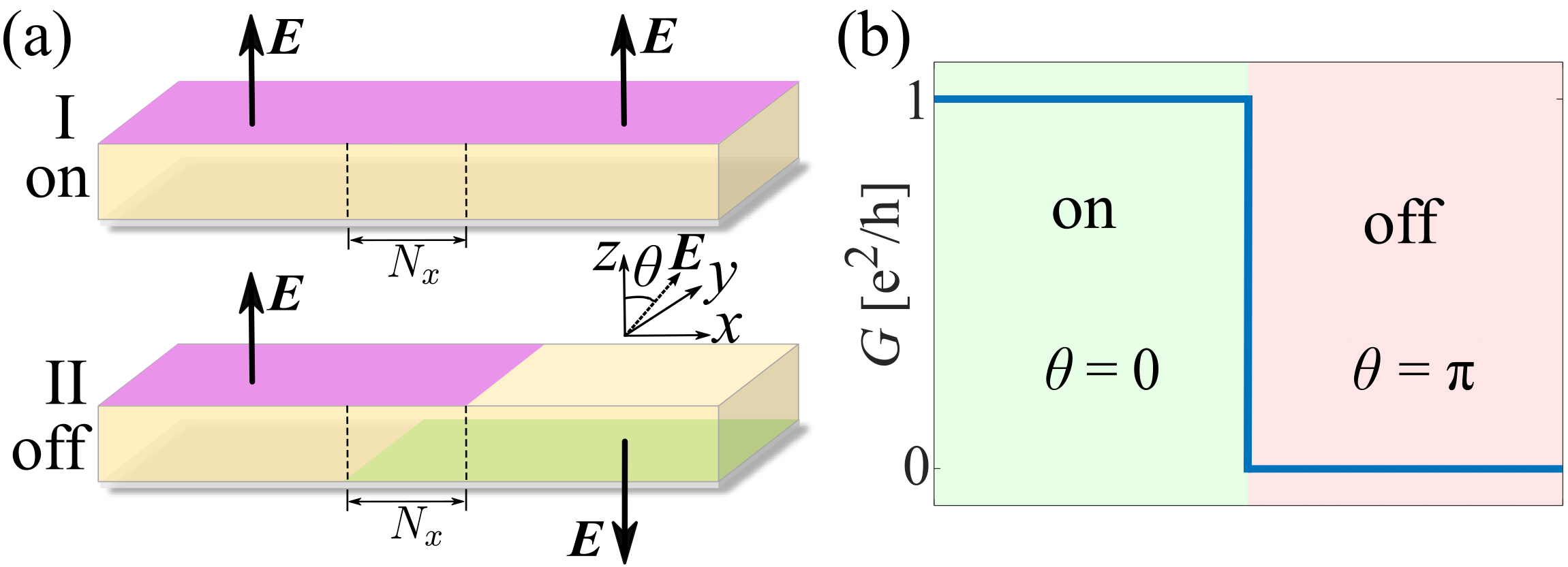
In this work, we propose a new on/off switching mechanism to realize a magnetic topological transistor based on the antiferromagnetic TI MnBi2Te4. This mechanism explores three crucial ingredients in MnBi2Te4: (i) topological Dirac surface states, (ii) intrinsic exchange fields, and (iii) layer degrees of freedom. To elucidate the physical picture, we first construct an effective model for MnBi2Te4 thin films in presence of external electric fields. We then show that manipulating the direction of electric fields allows us to selectively address the transport of top and bottom Dirac surface states. Exploiting this layer degree of freedom, we propose a two-terminal magnetic topological transistor. The “on” state (quantized conductance) and the “off” state (zero conductance) of this device are selected by the relative directions of two adjacent electric fields [Figs. 1(a)-(b)]. The physical reason is that we are able to guide the electron transport from the top surface state of the left region to either the top surface state of the right region (“on” state) or to the bottom surface state of the right region (“off” state). We show below that high on-off ratios () of the magnetic topological transistor can be achieved when the antiferromagnetic MnBi2Te4 films satisfy one of two criteria: (i) The films are thick enough to avoid hybridization of top and bottom surface states. (ii) The films have compensated antiferromagnetic order. In the latter case, the transistor can tolerate a considerable hybridization of top and bottom surface states due to their opposite Berry curvature. Our proposal requires electric control of MnBi2Te4, which has been demonstrated in recent experiments [37, 36].
II Effective model for surface states
To demonstrate the control of layer degrees of freedom by electric fields, we first construct an effective model of antiferromagnetic MnBi2Te4 thin films in presence of an electric field. MnBi2Te4 can be viewed as a TI with intrinsic antiferromagnetic order due to an exchange field [15, 24, 56], which breaks time-reversal symmetry. In practice, the electric field can be applied by dual gate technology [37]. Without loss of generality, we assume that the electric field is applied along direction and can be described by an electric potential , which is an odd function of , i.e., . This corresponds to symmetric gating at top and bottom surfaces. Asymmetric gating affects our results quantitatively but not qualitatively.
We start from the bulk Hamiltonian of three-dimensional (3D) TIs and derive the four lowest-energy eigenstates at the point as a basis [57, 58, 59, 60]. Then, we project the antiferromagnetic order and the electric potential into this basis. The resulting effective model for the MnBi2Te4 thin films in presence of the electric field can be written as [see Appendix A for more details]
| (1) |
where describes the Dirac surface states of TIs given by
| (2) |
with and . and are identity matrices and and with are Pauli matrices. The basis is {} with where represents top (bottom) surface states and represents spin up (down) states. and are model parameters that depend on the thickness of the films [see Appendix A]. For thick films, both and approach zero.
The second term in Eq. (1), i.e., , corresponds to the effective exchange field of the surface states. It opens a band gap in the spectrum of the Dirac surface states. Notably, the effective exchange field is different for even- and odd-layer thin films because of the antiferromagnetic order in the bulk. For even-layer films, the magnetization is compensated, whereas there is net magnetization for odd-layer films. As a result, reads
| (3) |
for odd-layer films, and
| (4) |
for even-layer films, where and are the corresponding strengths of the effective exchange field. The last term in Eq. (1) stems from the electric field. It reflects the structure inversion asymmetry (SIA) of the two surfaces described by
| (5) |
with being the SIA strength.
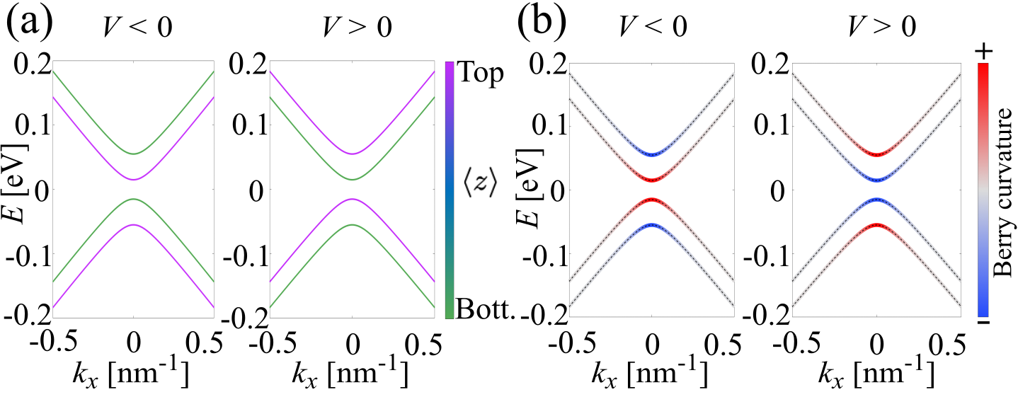
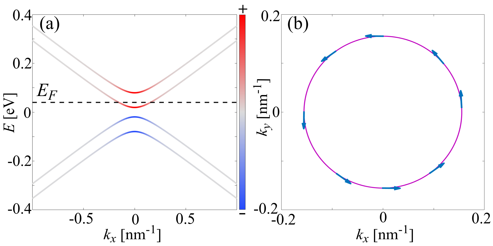
The SIA term induced by external electric fields can shift top and bottom surface states relative to each other in energy due to the potential difference at opposite surfaces, illustrated by the color-coded position expectation value for the low-energy bands in Fig. 2(a). Reversing the direction of the electric field, this alters the shift pattern in an opposite way. Note that the shift patterns of the surface energy bands are the same in films with odd and even layers. This can be understood by recasting the effective model in the basis of top and bottom surface states [see Appendix A for more details], i.e.,
| (6) |
where denote top and bottom surfaces, respectively, and indicates odd(even)-layer films. The new basis is {}. Note that the spin-momentum locking term in Eq. (6) is crucial for the robustness of surface state transport. For simplicity, we assume in Eq. (6) that the films are thick enough such that the hybridization of top and bottom surface states can be ignored (i.e., ). Evidently, the SIA strength has opposite signs for top and bottom surface states. Hence, it shifts the Dirac bands in an opposite way. If the Fermi level is placed to cross the lowest conduction band, then flipping the direction of the external electric field (changing the sign of ), this selects topological surface states from opposite surfaces.
Furthermore, the Berry curvature distributions of the surface states are strongly influenced by the SIA term . For even-layer films, in the absence of an electric field (), the Berry curvature of the lowest-energy band is zero due to the presence of PT symmetry (i.e., combined space inversion and time-reversal symmetry) [33]. When the electric field is present (), PT symmetry is broken. Hence, the degeneracy of the energy bands is lifted and the Berry curvature of each band becomes finite. In contrast, for odd-layer films, the Berry curvature is always nonzero due to the breaking of PT symmetry [19] no matter whether the electric field is present or not. Moreover, the Berry curvature of the even-layer films is layer-locked for conduction (or valence) bands [37], illustrated in Figs. 2(a) and 2(b).
III Magnetic topological transistor
We propose a magnetic topological transistor based on the unique properties described above [see Fig. 1(a) for a schematic]. The two side regions of the junction under the influence of external electric fields are connected to source and drain of the transistor. The middle region is free of external fields. Considering a finite-size 3D slab geometry, the topological surface bands evolve to quasi-1D spectra along the longitudinal direction. The relative energy separation of top and bottom quasi-1D spectra can be controlled by electric fields. This feature selects the layer degrees of freedom. The transistor can switch between “on” and “off” states depending on the relative direction of the electric fields, as illustrated in Fig. 1(b). When the electric fields are parallel, the transistor is in the “on” state with quantized conductance considering a single quasi-1D spectrum at the Fermi level. In contrast, when the electric fields are antiparallel, the transistor is in the “off” state with vanishing conductance .
The working principle of this transistor is based on layer degrees of freedom. At a given Fermi level, the top or bottom surface quasi-1D spectrum can solely be responsible for transport since the electric field separates different bands in energy [see Fig. 3(a)]. We set the direction of electric field on the left-hand side along direction such that the Fermi level only crosses the spectrum of the top surface. For the middle region of the transistor, the Fermi level crosses the spectrum of both top and bottom surfaces. Eventually, the nature of the conducting surface spectrum at the Fermi level on the right-hand side matters. If the top surface state on the right-hand side is responsible for transport [case I in Fig. 1(a)], then electrons traverse the junction easily and the conductance approaches . Otherwise [case II in Fig. 1(a)], the conductance approaches zero if the thickness of the middle region is large enough such that hybridization of top and bottom surface states is negligible. Note that although the surface states are gapped by the magnetic order, they inherit spin-momentum locking described by Eq. (2). Therefore, the back scattering from impurities is substantially suppressed.
IV Numerical simulations
Up to now, we have analyzed the mechanism for our proposed magnetic topological transistor from a thick-film perspective. To directly analyze the performance of the transistor for any film thickness, we perform numerical calculations based on the discretized 3D bulk Hamiltonian on a cubic lattice [see Appendix B], by employing the Landauer formalism [62, 63, 64]. We choose typical bulk parameters that are adopted to the material MnBi2Te4 based on ab initio calculations [15]. The chosen sample geometry consists of a cuboidal central region and two semi-infinite leads as source and drain. Exploiting the recursive Green function technique [65], the conductance of the setup can be evaluated by
| (7) |
where are the linewidth functions with the self-energy due to the coupling to the left/right lead. is the retarded (advanced) Green function of the central region.
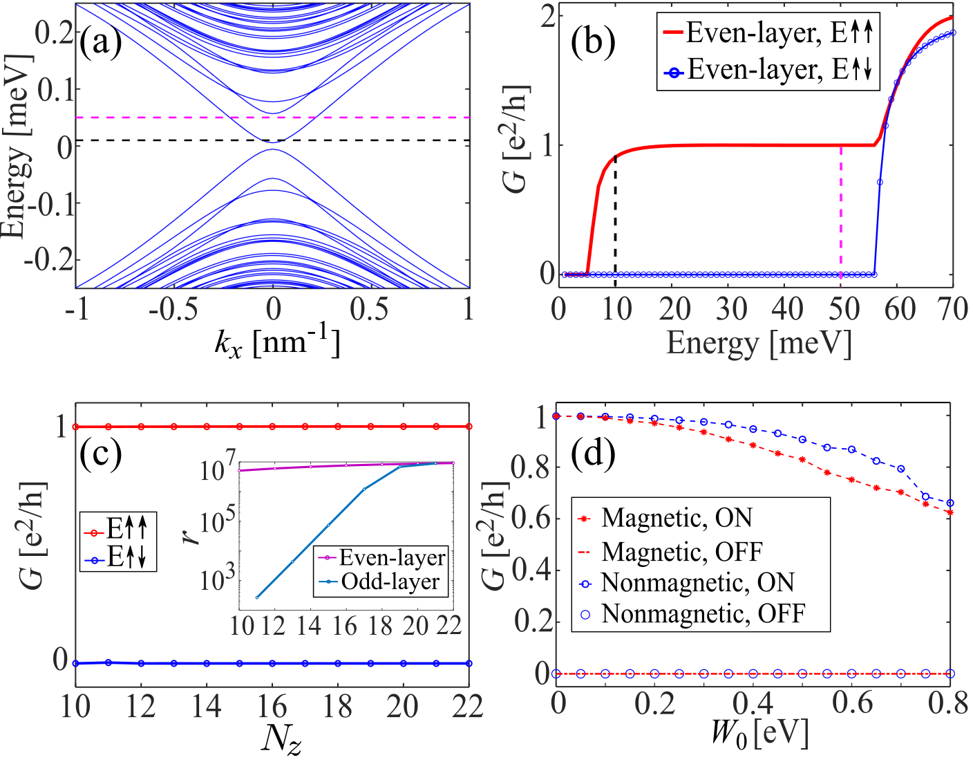
Figures 3(a) and 3(b) illustrate that the magnetic topological transistor works perfectly in a wide energy window, in which the conductance approaches for the “on” state (parallel configuration E) and decreases to nearly zero for the “off” state (antiparallel configuration E). Importantly, the range of this effective energy window is controllable by the strength of electric fields. This result is consistent with the phenomenological expectations discussed before. The on-off ratio of this transistor can reach , as shown in the inset of Fig. 3(c). When the Fermi level lies at the bottom of the quasi-1D spectrum, the value of decreases due to diminishing spin-momentum locking.
To obtain a large on-off ratio , the thickness of the junction should be large enough (i.e, ) to avoid hybridization of top and bottom surface states, as shown in the inset of Fig. 3(c). The on-off ratio increases as grows. Odd-layer devices only perform well for thick films while even-layer devices are less sensitive to the film thickness. Moreover, to illustrate the robustness of the magnetic topological transistor against perturbations, Anderson-type disorder is introduced through random on-site potential with a uniform distribution within , where denotes the disorder strength. It is evident from Fig. 3(d) that the proposed magnetic topological transistor persists to perform well in presence of disorders. The strong protection against perturbations comes from spin-momentum locking inherited from topological surface states. Moreover, the conductance is also robust against weak magnetic disorder. Note that the magnetic disorder in antiferromagnetic MnBi2Te4 may be formed by Mn sites filled with Bi atoms or Bi sites occupied by Mn atoms [66, 67, 68]. Therefore, the spin polarization of the magnetic disorder is considered along -direction in the calculation. For simplicity, we discuss the functionality of the magnetic topological transistor with a single conducting channel. When more channels are involved, the transistor works even better with higher on-off ratios [see Appendix C]. In our simulations, all the parameters are based on the ab initio calculations [15], which should apply to MnBi2Te4.
V Berry curvature features
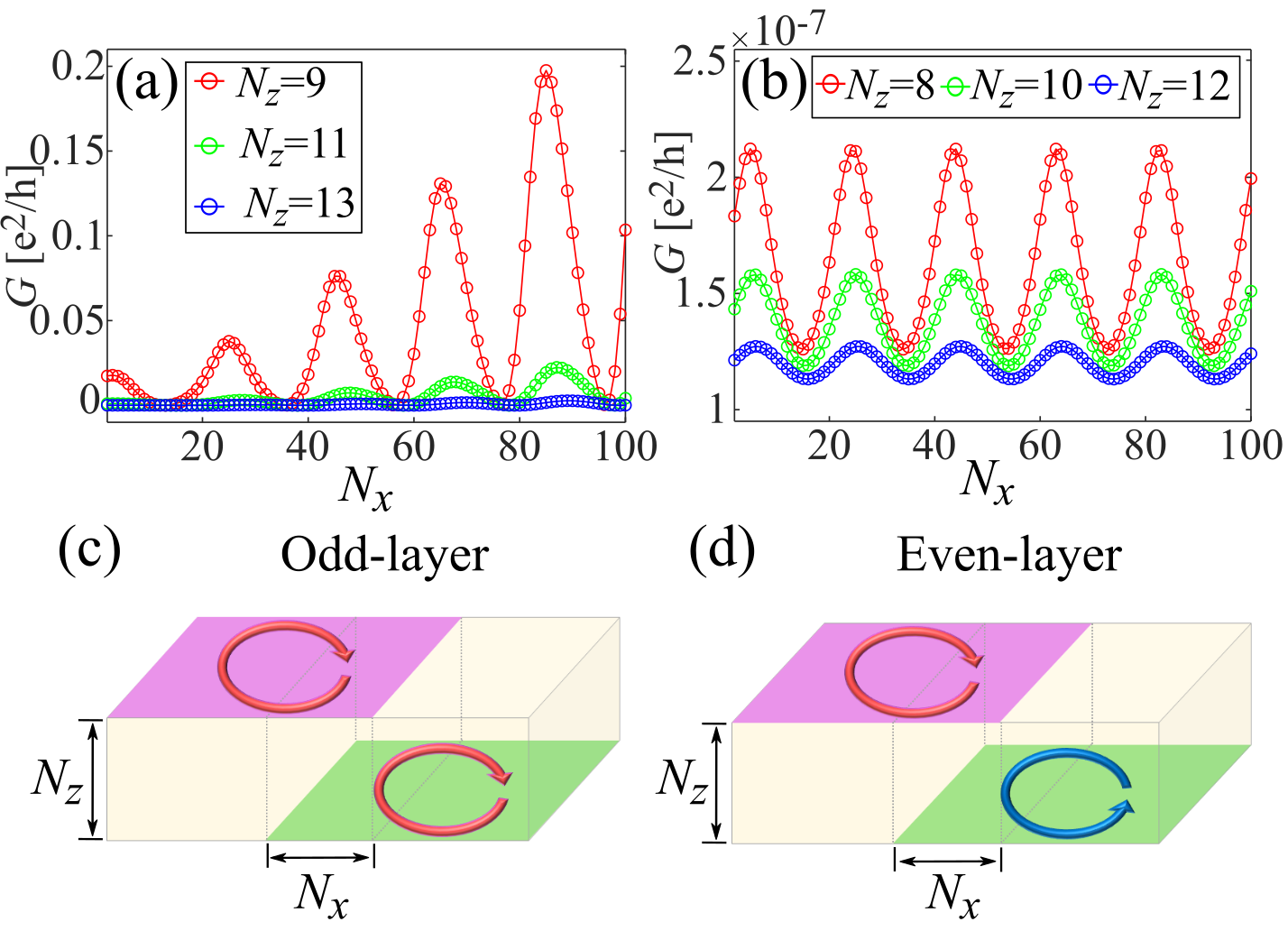
For thick films, the hybridization of top and bottom surface states is negligible. However, as the film thickness decreases, the hybridization of top and bottom surfaces becomes pronounced. The tunneling of the surface electrons from top to bottom diminishes the functionality of the magnetic topological transistor. Figure 4(a) shows that the conductance oscillates (as a function of ) with finite amplitude as the thickness of the transistor decreases in odd-layer thin films. In striking contrast, the conductance of the even-layer thin films stays close to zero (of the order of 10-7 e2/h) even when is quite small [Fig. 4(b)]. The different behaviors between odd and even layer cases originate from the spin polarization of top and bottom surface states. For a given Fermi energy intersecting the conduction band, the spin polarization is the same for odd-layer films but opposite for even-layer case in agreement with the direction of the magnetization. This is featured by the same Berry curvature distribution for odd-layer system [Fig. 4(c)] and the opposite Berry curvature distribution for even-layer system [Fig. 4(d)]. We show in Appendix C that this difference of the Berry curvature distribution crucially affects the transport properties in the “off” state. Consequently, even-layer thin film devices are superior as compared to odd-layer thin film devices.
VI Conclusion
We have developed an effective model for the antiferromagnetic TI MnBi2Te4 in presence of electric fields to demonstrate that electric fields can be exploited to selectively guide surface state transport. We have proposed a magnetic topological transistor based on three crucial ingredients: topology (for the emergence of surface states with strong spin-momentum locking), exchange fields (to gap the surface states), and electric-field-controllable layer degrees of freedom (to select top and bottom surface states). The proposed magnetic topological transistor is robust against disorder due to strong spin-momentum locking of the surface states. It shows large on-off ratios when the magnetic TI films are thick enough to avoid hybridization or have fully compensated magnetic order. Our work suggests a new switching mechanism for transistors exploiting layer-selective transport.
Acknowledgements.
We thank Rui Chen for valuable discussions. This work was supported by the DFG (SPP1666 and SFB1170 “ToCoTronics”), the Würzburg-Dresden Cluster of Excellence ct.qmat, EXC2147, Project No. 390858490, and the Elitenetzwerk Bayern Graduate School on “Topological Insulators”. We thank the Bavarian Ministry of Economic Affairs, Regional Development and Energy for financial support within the High-Tech Agenda Project “Bausteine für das Quanten Computing auf Basis topologischer Materialen”. S.B.Z acknowledges the support by the UZH Postdoc Grant. H.Z.L. acknowledges support by the National Natural Science Foundation of China (Grant No. 11925402).Appendix A Effective model for surface states
A.1 3D bulk Hamiltonian for antiferromagnetic MnBi2Te4 in presence of an electric field
The 3D bulk Hamiltonian in presence of an external electric field for antiferromagnetic topological insulators (TIs) MnBi2Te4 reads
| (8) |
where is the nonmagnetic part, is the exchange field that accounts for the out-of-plane antiferromagnetic order, and is the electric potential induced by the external electric field. The non-magnetic part is given by [15]
| (9) |
with , and . , , , and are model parameters with . The basis of the Hamiltonian is {}.
The exchange field reads
| (10) |
where is the magnetization energy along -direction with the amplitude of the intralayer ferromagnetic order. is the thickness of a septuple layer. is the Pauli matrix for spin degrees of freedom, and is a 22 identity matrix for orbital degrees of freedom.
We assume the electric potential is an odd function of , namely, , which corresponds to symmetric gating. The qualitative findings of ours are not affected by this choice.
A.2 Wave functions and eigen energies for MnBi2Te4 thin films
Consider a MnBi2Te4 thin film with thickness along direction and label bottom and top boundaries as and , respectively. First, we derive the surface eigenstates of the nonmagnetic part at the point (), which form the basis for the effective model. Replacing by , since is no longer a good quantum number, and taking in , we arrive at , where
| (11) |
with . The general eigenstate for reads
| (12) |
where
| (13) | |||
| (14) |
with , , , , , and .
Using open boundary conditions at , namely, , we obtain the transcendental equations for the eigenenergies
| (15) | |||||
| (16) |
Moreover, we find the wave functions from the general solution as
| (17) | |||||
| (18) |
with
| (19) | |||
| (20) | |||
| (21) | |||
| (22) |
and are the normalization coefficients. Thus, the wave functions for in Eq.(11) read
| (23) | |||||
| (24) |
A.3 Effective model for MnBi2Te4 thin films in presence of an electric field
Projecting the 3D bulk Hamiltonian for MnBi2Te4 to the basis {}, we obtain the effective model as
| (25) | |||||
where
| (26) |
with , , , , , , , , and . For simplicity, we have ignored the energy shift and the particle-hole asymmetry term , which implies that in Eq.(9).
The effective exchange field for odd-layer thin films reads
| (27) |
where with the number of layers.
The effective exchange field for even-layer thin films reads
| (28) |
where with the number of layers. In Eqs.(27) and (28), and are the strengths of the effective exchange field for the surface states of odd- and even-layer thin films, respectively. and are not the same because of the different profiles of bulk magnetization.
Structure inversion asymmetry (SIA) induced by the electric field is described by
| (29) |
where is the strength of SIA.
In summary, the effective model for odd-layer MnBi2Te4 thin films in presence of electric fields reads
with , and .
Likewise, the effective model for even-layer MnBi2Te4 thin films reads
Note that the basis of the model is a mixture of top and bottom surface states as {} with .
The parameters of the effective model for antiferromagnetic MnBi2Te4 thin films used in Fig. 2 are shown below. Note that the parameters for the effective model are obtained from the bulk parameters extracted from ab initio calculations [15]. For the even-layer film with , the parameters are meV, 1.31 meVnm2, 319.64 meVnm, 0 meV, 35.02 meV, 20 meV. For the odd-layer film with , the parameters are meV, 0.67 meVnm2, 319.64 meVnm, 35.02 meV, 0 meV, 20 meV.
A.4 Effective model for MnBi2Te4 thick films
For MnBi2Te4 thick films, the parameters and approach zero, which implies that . The unitary transformation is used to transform the basis as
| (30) |
with . Thus, the new basis is . Here, the unitary operator reads
| (31) |
Thus the new basis is {}. The effective model for odd-layer MnBi2Te4 thick films in the new basis reads
Similarly, the effective model for even-layer MnBi2Te4 thick films in the new basis reads
A.5 Spin texture of the effective model
Appendix B Lattice model for magnetic TIs in presence of electric fields
The effective Hamiltonian of Eq.(8) can be regularized on a cubic lattice by the substitutions , , where is the lattice constant and . For simplicity, we take nm. The three lattice translation vectors are defined as . The lattice model for antiferromagnetic MnBi2Te4 reads
| (32) |
where
| (33) |
with for , and . and are Pauli matrices for the spin and orbital degrees of freedom, respectively, , , , and . The exchange field reads
| (34) |
For the antiferromagnetic MnBi2Te4, we introduce a sublayer index to describe the unit-cell doubling and characterize the magnetization in sublayer by with angles and . The A-type antiferromagnetic order is described by and , where
| (35) |
The electric potential is , where depicts the strength of the electric field. In the lattice model, the electric potential difference of neighboring layers is .

Appendix C More transport results
C.1 More results for intrinsic antiferromagnetic TIs
C.2 Scattering matrix theory
By combining the scattering matrices , and illustrated in Fig. 7 (a), we obtain the scattering matrix connecting the states . We solve the scattering problem using the one-dimensional effective Hamiltonian. As shown in Fig. 7(a), the right-moving mode in the top layer is reflected at the right edge, while the left-moving mode is reflected at the left edge. These scattering processes are described by and . Namely, and model the barriers in the middle region.
The scattering matrix is obtained by solving two copies of the scattering problem: one is between and the other is between , each with the Hamiltonian . Consequently, is
| (36) |
where and are the scattering amplitudes. The scattering matrix connects only the scattering states with . Similarly, the scattering states on the bottom layer are connected by .
Combining the partial scattering matrices , , and , the full scattering matrix becomes
| (37) |
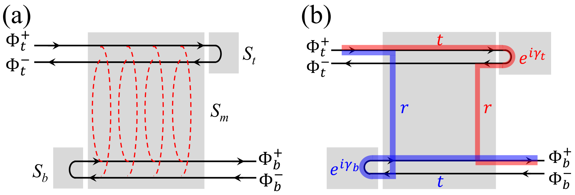
The transmission probability for the incoming state on the top layer to be transmitted to the outgoing mode on the bottom layer reads
| (38) |
with . Therefore, can be understood in terms of quantum interference illustrated in Fig. 7(b).
We solve the scattering problem to obtain the phase difference . The reflection phase at the top layer is obtained by solving . In particular, the reflection phase is
| (39) |
where the spin state refers to the oppositely polarized state of . The second term can be interpreted as a geometric phase calculated by integrating the Berry connection along the geodesic connecting three spin states , , and on the Bloch sphere. Similarly, for the bottom layer, we solve the scattering problem . The reflection phase is
| (40) |
In total,
| (41) |
Finally, we obtain the quantum phase
| (42) |
Hence, the transmission probability is
| (43) |
The interference at odd and even layers occurs constructively and destructively, respectively. Hence, the transmission is finite for the odd layers. On the contrary, for the even layers, the destructive interference suppresses the transport.
References
- Moore [2010] J. E. Moore, “The birth of topological insulators”, Nature 464, 194 (2010).
- Hasan and Kane [2010] M. Z. Hasan and C. L. Kane, “Colloquium: Topological insulators”, Rev. Mod. Phys. 82, 3045 (2010).
- Qi and Zhang [2011] X.-L. Qi and S.-C. Zhang, “Topological insulators and superconductors”, Rev. Mod. Phys. 83, 1057 (2011).
- Xue [2011] Q.-K. Xue, “A topological twist for transistors”, Nat. Nanotechnol. 6, 197 (2011).
- Xiu et al. [2011] F. Xiu, et al., “Manipulating surface states in topological insulator nanoribbons”, Nat. Nanotechnol. 6, 216 (2011).
- Wray [2012] L. A. Wray, “Topological transistor”, Nat. Phys. 8, 705 (2012).
- Checkelsky et al. [2012] J. G. Checkelsky, J. Ye, Y. Onose, Y. Iwasa, and Y. Tokura, “Dirac-fermion-mediated ferromagnetism in a topological insulator”, Nat. Phys. 8, 729 (2012).
- Yu et al. [2010] R. Yu, W. Zhang, H.-J. Zhang, S.-C. Zhang, X. Dai, and Z. Fang, “Quantized Anomalous Hall Effect in Magnetic Topological Insulators”, Science 329, 61 (2010).
- Michetti and Trauzettel [2013] P. Michetti and B. Trauzettel, “Devices with electrically tunable topological insulating phases”, Appl. Phys. Lett. 102, 063503 (2013).
- Qian et al. [2014] X. Qian, J. Liu, L. Fu, and J. Li, “Quantum spin Hall effect in two-dimensional transition metal dichalcogenides”, Science 346, 1344 (2014).
- Liu et al. [2014] J. Liu, T. H. Hsieh, P. Wei, W. Duan, J. Moodera, and L. Fu, “Spin-filtered edge states with an electrically tunable gap in a two-dimensional topological crystalline insulator”, Nat. Mater. 13, 178 (2014).
- Wang et al. [2015] J. Wang, B. Lian, and S.-C. Zhang, “Electrically Tunable Magnetism in Magnetic Topological Insulators”, Phys. Rev. Lett. 115, 036805 (2015).
- Liu et al. [2015] Q. Liu, X. Zhang, L. B. Abdalla, A. Fazzio, and A. Zunger, “Switching a Normal Insulator into a Topological Insulator via Electric Field with Application to Phosphorene”, Nano Lett. 15, 1222 (2015).
- Collins et al. [2018] J. L. Collins, et al., “Electric-field-tuned topological phase transition in ultrathin Na3Bi”, Nature 564, 390 (2018).
- Zhang et al. [2019] D. Zhang, M. Shi, T. Zhu, D. Xing, H. Zhang, and J. Wang, “Topological Axion States in the Magnetic Insulator MnBi2Te4 with the Quantized Magnetoelectric Effect”, Phys. Rev. Lett. 122, 206401 (2019).
- Otrokov et al. [2019a] M. M. Otrokov, et al., “Prediction and observation of an antiferromagnetic topological insulator”, Nature 576, 416 (2019a).
- Rienks et al. [2019] E. D. L. Rienks, et al., “Large magnetic gap at the Dirac point in Bi2Te3/MnBi2Te4 heterostructures”, Nature 576, 423 (2019).
- Gong et al. [2019] Y. Gong, et al., “Experimental Realization of an Intrinsic Magnetic Topological Insulator”, Chinese Phys. Lett. 36, 076801 (2019).
- Li et al. [2019a] J. Li, Y. Li, S. Du, Z. Wang, B.-L. Gu, S.-C. Zhang, K. He, W. Duan, and Y. Xu, “Intrinsic magnetic topological insulators in van der Waals layered MnBi2Te4-family materials”, Sci. Adv. 5, eaaw5685 (2019a).
- Otrokov et al. [2019b] M. M. Otrokov, I. P. Rusinov, M. Blanco-Rey, M. Hoffmann, A. Y. Vyazovskaya, S. V. Eremeev, A. Ernst, P. M. Echenique, A. Arnau, and E. V. Chulkov, “Unique Thickness-Dependent Properties of the van der Waals Interlayer Antiferromagnet MnBi2Te4 Films”, Phys. Rev. Lett. 122, 107202 (2019b).
- Sun et al. [2019] H. Sun, B. Xia, Z. Chen, Y. Zhang, P. Liu, Q. Yao, H. Tang, Y. Zhao, H. Xu, and Q. Liu, “Rational Design Principles of the Quantum Anomalous Hall Effect in Superlatticelike Magnetic Topological Insulators”, Phys. Rev. Lett. 123, 096401 (2019).
- Lei et al. [2020] C. Lei, S. Chen, and A. H. MacDonald, “Magnetized topological insulator multilayers”, Proceedings of the National Academy of Sciences 117, 27224 (2020).
- Wang et al. [2020] H. Wang, D. Wang, Z. Yang, M. Shi, J. Ruan, D. Xing, J. Wang, and H. Zhang, “Dynamical axion state with hidden pseudospin Chern numbers in MnBi2Te4-based heterostructures”, Phys. Rev. B 101, 081109 (2020).
- Zhang et al. [2020] R.-X. Zhang, F. Wu, and S. Das Sarma, “Möbius Insulator and Higher-Order Topology in MnBi2nTe3n+1”, Phys. Rev. Lett. 124, 136407 (2020).
- Lian et al. [2020] B. Lian, Z. Liu, Y. Zhang, and J. Wang, “Flat Chern Band from Twisted Bilayer MnBi2Te4”, Phys. Rev. Lett. 124, 126402 (2020).
- Lei and MacDonald [2021] C. Lei and A. H. MacDonald, “Gate-tunable quantum anomalous Hall effects in MnBi2Te4 thin films”, Phys. Rev. Materials 5, L051201 (2021).
- Wei et al. [2021] B. Wei, J.-J. Zhu, Y. Song, and K. Chang, “Renormalization of gapped magnon excitation in monolayer MnBi2Te4 by magnon-magnon interaction”, Phys. Rev. B 104, 174436 (2021).
- Varnava et al. [2021] N. Varnava, J. H. Wilson, J. H. Pixley, and D. Vanderbilt, “Controllable quantum point junction on the surface of an antiferromagnetic topological insulator”, Nat. Commun. 12, 3998 (2021).
- Gu et al. [2021] M. Gu, J. Li, H. Sun, Y. Zhao, C. Liu, J. Liu, H. Lu, and Q. Liu, “Spectral signatures of the surface anomalous Hall effect in magnetic axion insulators”, Nat. Commun. 12, 3524 (2021).
- Li et al. [2021] H. Li, C.-Z. Chen, H. Jiang, and X. C. Xie, “Coexistence of Quantum Hall and Quantum Anomalous Hall Phases in Disordered MnBi2Te4”, Phys. Rev. Lett. 127, 236402 (2021).
- Chen et al. [2021a] R. Chen, S. Li, H.-P. Sun, Q. Liu, Y. Zhao, H.-Z. Lu, and X. C. Xie, “Using nonlocal surface transport to identify the axion insulator”, Phys. Rev. B 103, L241409 (2021a).
- Chen et al. [2021b] W. Chen, Y. Zhao, Q. Yao, J. Zhang, and Q. Liu, “Koopmans’ theorem as the mechanism of nearly gapless surface states in self-doped magnetic topological insulators”, Phys. Rev. B 103, L201102 (2021b).
- Du et al. [2020] S. Du, P. Tang, J. Li, Z. Lin, Y. Xu, W. Duan, and A. Rubio, “Berry curvature engineering by gating two-dimensional antiferromagnets”, Phys. Rev. Research 2, 022025 (2020).
- Liu and Wang [2020] Z. Liu and J. Wang, “Anisotropic topological magnetoelectric effect in axion insulators”, Phys. Rev. B 101, 205130 (2020).
- Liu et al. [2021a] Z. Liu, D. Qian, Y. Jiang, and J. Wang, “Dissipative Edge Transport in Disordered Axion Insulator Films”, (2021a), arXiv:2109.06178 .
- Cai et al. [2022] J. Cai, et al., “Electric control of a canted-antiferromagnetic Chern insulator”, Nat. Commun. 13, 1668 (2022).
- Gao et al. [2021] A. Gao, et al., “Layer Hall effect in a 2D topological axion antiferromagnet”, Nature 595, 521 (2021).
- Liu et al. [2021b] C. Liu, et al., “Magnetic-field-induced robust zero Hall plateau state in MnBi2Te4 Chern insulator”, Nat. Commun. 12, 4647 (2021b).
- Chen et al. [2019a] B. Chen, et al., “Intrinsic magnetic topological insulator phases in the Sb doped MnBi2Te4 bulks and thin flakes”, Nat. Commun. 10, 4469 (2019a).
- Hao et al. [2019] Y.-J. Hao, et al., “Gapless Surface Dirac Cone in Antiferromagnetic Topological Insulator MnBi2Te4”, Phys. Rev. X 9, 041038 (2019).
- Li et al. [2019b] H. Li, et al., “Dirac Surface States in Intrinsic Magnetic Topological Insulators EuSn2As2 and MnBi2nTe3n+1”, Phys. Rev. X 9, 041039 (2019b).
- Chen et al. [2019b] Y. J. Chen, et al., “Topological Electronic Structure and Its Temperature Evolution in Antiferromagnetic Topological Insulator MnBi2Te4”, Phys. Rev. X 9, 041040 (2019b).
- Swatek et al. [2020] P. Swatek, Y. Wu, L.-L. Wang, K. Lee, B. Schrunk, J. Yan, and A. Kaminski, “Gapless Dirac surface states in the antiferromagnetic topological insulator MnBi2Te4”, Phys. Rev. B 101, 161109 (2020).
- Wu et al. [2020] X. Wu, et al., “Distinct Topological Surface States on the Two Terminations of MnBi4Te7”, Phys. Rev. X 10, 031013 (2020).
- Lu et al. [2021] R. Lu, et al., “Half-Magnetic Topological Insulator with Magnetization-Induced Dirac Gap at a Selected Surface”, Phys. Rev. X 11, 011039 (2021).
- Vidal et al. [2021] R. C. Vidal, et al., “Orbital Complexity in Intrinsic Magnetic Topological Insulators MnBi4Te7 and MnBi6Te”, Phys. Rev. Lett. 126, 176403 (2021).
- Lee et al. [2021] S. H. Lee, et al., “Evidence for a Magnetic-Field-Induced Ideal Type-II Weyl State in Antiferromagnetic Topological Insulator Mn(Bi1-xSbx)2Te4”, Phys. Rev. X 11, 031032 (2021).
- Deng et al. [2020] Y. Deng, Y. Yu, M. Z. Shi, Z. Guo, Z. Xu, J. Wang, X. H. Chen, and Y. Zhang, “Quantum anomalous Hall effect in intrinsic magnetic topological insulator MnBi2Te4”, Science 367, 895 (2020).
- Liu et al. [2020] C. Liu, Y. Wang, H. Li, Y. Wu, Y. Li, J. Li, K. He, Y. Xu, J. Zhang, and Y. Wang, “Robust axion insulator and Chern insulator phases in a two-dimensional antiferromagnetic topological insulator”, Nat. Mater. 19, 522 (2020).
- Deng et al. [2021] H. Deng, et al., “High-temperature quantum anomalous Hall regime in a MnBi2Te4/Bi2Te3 superlattice”, Nat. Phys. 17, 36 (2021).
- Ge et al. [2020] J. Ge, Y. Liu, J. Li, H. Li, T. Luo, Y. Wu, Y. Xu, and J. Wang, “High-Chern-number and high-temperature quantum Hall effect without Landau levels”, Natl. Sci. Rev. 7, 1280 (2020).
- Ovchinnikov et al. [2021] D. Ovchinnikov, et al., “Intertwined Topological and Magnetic Orders in Atomically Thin Chern Insulator MnBi2Te4”, Nano Lett. 21, 2544 (2021).
- Ge et al. [2022] J. Ge, Y. Liu, P. Wang, Z. Xu, J. Li, H. Li, Z. Yan, Y. Wu, Y. Xu, and J. Wang, “Magnetization-tuned topological quantum phase transition in MnBi2Te4 devices”, Phys. Rev. B 105, L201404 (2022).
- Liang et al. [2022] A. Liang, et al., “Approaching a Minimal Topological Electronic Structure in Antiferromagnetic Topological Insulator MnBi2Te4 via Surface Modification”, Nano Lett. 22, 4307 (2022).
- Lei et al. [2022] X. Lei, et al., “Magnetically tunable Shubnikov–de Haas oscillations in MnBi2Te4”, Phys. Rev. B 105, 155402 (2022).
- Zhang et al. [2009] H. Zhang, C.-X. Liu, X.-L. Qi, X. Dai, Z. Fang, and S.-C. Zhang, “Topological insulators in Bi2Se3, Bi2Te3 and Sb2Te3 with a single Dirac cone on the surface”, Nat. Phys. 5, 438 (2009).
- Sun et al. [2020] H.-P. Sun, C. M. Wang, S.-B. Zhang, R. Chen, Y. Zhao, C. Liu, Q. Liu, C. Chen, H.-Z. Lu, and X. C. Xie, “Analytical solution for the surface states of the antiferromagnetic topological insulator MnBi2Te4”, Phys. Rev. B 102, 241406 (2020).
- Lu et al. [2013] H.-Z. Lu, A. Zhao, and S.-Q. Shen, “Quantum Transport in Magnetic Topological Insulator Thin Films”, Phys. Rev. Lett. 111, 146802 (2013).
- Shan et al. [2010] W.-Y. Shan, H.-Z. Lu, and S.-Q. Shen, “Effective continuous model for surface states and thin films of three-dimensional topological insulators”, New J. Phys. 12, 043048 (2010).
- Lu et al. [2010] H.-Z. Lu, W.-Y. Shan, W. Yao, Q. Niu, and S.-Q. Shen, “Massive Dirac fermions and spin physics in an ultrathin film of topological insulator”, Phys. Rev. B 81, 115407 (2010).
- [61] Numerical transport calculations are based on the discretized 3D bulk Hamiltonian on a cubic lattice. The bulk parameters are adopted to the material MnBi2Te4 as =270.23 meVnm, =319.64 meVnm, =-119.05 meVnm2, =-94.05 meVnm2, =-116.50 meV, =50 meV. Here, we choose the parameter meV in Figs. 3(a), 3(b) and 3(d) and Figs. 4(a) and 4(b), and meV in Fig. 3(c). The system size is and unless specified .
- Landauer [1970] R. Landauer, “Electrical resistance of disordered one-dimensional lattices”, The Philosophical Magazine 21, 863 (1970).
- Büttiker [1986] M. Büttiker, “Four-Terminal Phase-Coherent Conductance”, Phys. Rev. Lett. 57, 1761 (1986).
- Datta [1997] S. Datta, Electronic Transport in Mesoscopic Systems (Cambridge University Press, 1997).
- MacKinnon [1985] A. MacKinnon, “The calculation of transport properties and density of states of disordered solids”, Z. Physik B - Condensed Matter 59, 385 (1985).
- Zeugner et al. [2019] A. Zeugner, et al., “Chemical Aspects of the Candidate Antiferromagnetic Topological Insulator MnBi2Te4”, Chem. Mater. 31, 2795 (2019).
- Shikin et al. [2021] A. M. Shikin, et al., “Sample-dependent Dirac-point gap in MnBi2Te4 and its response to applied surface charge: A combined photoemission and ab initio study”, Phys. Rev. B 104, 115168 (2021).
- Garnica et al. [2022] M. Garnica, et al., “Native point defects and their implications for the Dirac point gap at MnBi2Te4 (0001)”, npj Quantum Mater. 7, 1 (2022).