Interplay of quantum confinement and strain effects in type I to type II transition in Ge/Si core-shell nanocrystals
Abstract
The electronic properties of hydrogenated, spherical, Si/Ge and Ge/Si core-shell nanocrystals with a diameter ranging from to nm are studied within Density Functional Theory. Effects induced by quantum confinement and strain on the near-band-edge states localization, as well as the band-offset properties between Si and Ge regions, are investigated in detail. On the one hand, we prove that Si(core)/Ge(shell) nanocrystals always show a type II band-offset alignment, with the HOMO mainly localized on the Ge shell region and the LUMO mainly localized on the Si core region. On the other hand, our results point out that a type II offset cannot be observed in small (diameter less than nm) Ge(core)/Si(shell) nanocrystals. In these systems, quantum confinement and strain drive the near-band-edge states to be mainly localized on Ge atoms inducing a type I alignment. In larger Ge(core)/Si(shell) nanocrystals, instead, the formation of a type II offset can be engineered by playing with both core and shell thickness. The conditions that favor the transition from a type I to a type II alignment for Ge(core)/Si(shell) nanocrystals are discussed in detail.
I Introduction
The electronic, transport and optical properties of silicon (Si) and germanium (Ge) nanomaterials have been largely investigated in the past, both experimentally and theoretically, due to their promising applications in optoelectronics and photovoltaics [1, 2, 3, 4, 5, 6, 7, 8, 9, 10, 11, 12, 13, 14, 15, 16, 17, 18, 19, 20, 21, 22, 23, 24, 25, 26]. Moreover, it has been shown that Si and Ge can be combined to obtain innovative materials that can be easily integrated into existing devices. Compared to pure Si and Ge materials, Si/Ge heterostructures offer more possibilities to tune the above-said properties [27, 28]. This can be achieved by varying Si and Ge atoms concentration and their spatial disposition, by modifying the geometry of Si/Ge interface and by modulating both strain and the quantum confinement effect (QCE) to obtain systems with the desired properties.
Si/Ge heterostructures have been fabricated using different techniques, such as molecular beam epitaxy [29], self-assembly [30, 31], ion beam and magnetic sputtering deposition [32, 33, 34, 35], chemical vapor deposition [36, 37], chemical synthesis [38] and gas-phase and nonthermal plasma synthesis [39, 40, 41]. They have been integrated into different technological devices, for instance in high-speed and high-power field-effect transistors [42, 43, 44, 45, 46], photodetectors [47, 48], linear and non-linear optics devices [49, 50], solar cell systems [51, 52], non-volatile memory [53] and thermoelectric [54] devices.
Nowadays, the research focused on Si/Ge nanosystems, in particular core-shell (CS) nanowires (NWs) [55, 56, 57, 58] and nanocrystals (NCs) [59, 60, 61], represents one of the most rapidly developing areas in materials science.
CS nanosystems offer the possibility of engineering electronic and optical properties by varying core diameter and shell thickness [62, 63, 64] (thus modulating strain and QCE of both core and shell regions) and by switching core and shell materials.
Particular attention has been dedicated to the study of the band-offset properties of Si/Ge and Ge/Si CSNCs, a fundamental step to understand the relative localization of electrons and holes. The alignment of energy levels of both core and shell materials can result in type I (band-edges localized on the same material) or in type II (band-edges localized on different materials) heterostructures.
Type I materials show a strong overlap between electron and hole wavefunctions, that can be exploited in light-emitting devices.
Type II alignment shows, instead, a weaker overlap between electron and hole wavefunctions which are, in this case, localized on different materials. This induces longer radiative lifetimes, lower excitation binding energies and smaller exciton oscillator strengths when compared to type I structures.
Leading to a reduction of non-radiative Auger recombination rates - because of the favored photogenerated charge carriers separation and their extraction - type II heterostructures are of great interest for photovoltaics applications [65].
Energy levels alignment between Si and Ge bulks reveals a type II offset for Si/Ge superlattice heterostructures, a band-edge profile that, however, can be altered by strain and QC when low dimensionality is taken into account.
Band-offset properties of Si/Ge and Ge/Si CSNCs were extensively studied theoretically, with results not always consistent with each other.
A type II confinement, with electrons localized in the Si regions and holes localized in the Ge regions, was predicted for small Si/Ge and Ge/Si CSNCs by Ramos et al. [62]. A similar result was obtained by de Oliveira et al. [66], through the analysis of the radial distribution of the HOMO and LUMO orbitals. However, while the formation of a type II offset was clearly proved for the Si(core)/Ge(shell) NCs, it was less evident for the Ge(core)/Si(shell) NCs. The formation of a type II offset in small Ge(core)/Si(shell) NCs was questioned by Nestoklon et al. [67]. By adopting a tight-binding model to study systems of different core and shell extensions, they always observed a strong localization of the LUMO state in the Ge core region for structures with a thin Si shell (thickness below 0.8 nm).
Finally, a type II band-offset was predicted, using tight-binding methods, by Neupane et al. for large spherical Ge(core)/Si(shell) NCs with diameters ranging from 11 to 17.5 nm [68] and for large dome-shaped GeSi CSNCs [69, 70].
Theoretical works agree therefore in indicating a type II offset for both Si(core)/Ge(shell) and large Ge(core)/Si(shell) NCs but do not uniquely define the band-offset properties of small Ge(core)/Si(shell) NCs. Moreover, an unambiguous description of the band alignment characteristics of Ge(core)/Si(shell) NCs as a function of the NCs size is still missing.
In this work, we consider Si(core)/Ge(shell) and Ge(core)/Si(shell) NCs of different sizes and compositions and we clarify the mechanisms behind the formation of a type II offset, shedding light on the role played by the QCE and strain. To conduct our investigation, we adopt two different approaches. In the first one, the whole CSNC is taken into account without any simplification. This approach is used to obtain a quantitative signature of the band-offset. In the second method, core and shell are analyzed separately, thus adopting an approach that allows to better clarify the role played by both QC (see Sect. III.3) and strain (see Sect. III.4).
II Method
The structural and electronic properties of different spherical, Si(core)/Ge(shell) and Ge(core)/Si(shell) NCs, with diameters ranging from 1.8 to 4.0 nm, have been investigated by means of first-principles calculations. Only hydrogenated NCs have been considered, thus avoiding configurations leading to the formation of near-band-edge surface states. For all the considered systems, we have performed Density Functional Theory (DFT) calculations using the Local Density Approximation (LDA) for the exchange-correlation functional, as implemented in the plane-wave pseudopotential Quantum ESPRESSO (QE)[71, 72] code. A careful analysis of the convergence of both structural and electronic properties, in terms of plane-wave basis set cutoff, has been conducted. Norm-conserving pseudopotentials with a kinetic cutoff for the plane-wave basis set of 40 Ry have been adopted for all the considered systems. NCs have been placed in large cubic cells containing a large amount of vacuum to avoid spurious interactions between replicas. All atomic positions in the supercells have been fully relaxed until the forces acting on each atom were less than 0.003 Ry/a.u. Si(core)/Ge(shell) and Ge(core)/Si(shell) band-edge properties have been determined by analyzing the localization of Kohn-Sham (KS) HOMO and LUMO states, as done in previous studies (see for example Ref. [73]). For one of the smallest NCs (Ge35Si112H100), the band offsets were also estimated within the GW approximation, to check if the DFT-KS band ordering could be affected by many-body effects. Calculations have been performed adopting 80000 plane waves for the calculation of the exchange part of the self-energy and 30000 plane waves for both the screening and the correlation part of the self-energy . The total number of bands was set to 2500 for and to 3700 for [74]. A spherical cut of the Coulomb interaction was used to avoid spurious interactions between periodic replicas. Noticeably, obtained results point out that DFT outcomes are not altered by the inclusion of GW corrections. More details are reported in Sect. V.
III Results
In the following, we focus our attention on the study of the band-offset properties of Si(core)/Ge(shell) and Ge(core)/Si(shell) NCs of different sizes. The section is divided into four parts. In Sect. III.1, we discuss the intrinsic properties of Si and Ge materials. In Sect. III.2, we analyse the band-offset properties of Si/Ge and Ge/Si CSNCs with diameters ranging from to nm. In Sect. III.3 we compare the effects induced by the confinement of the electronic charge density on the electronic properties of systems of different shapes but with the same number of atoms. Finally, in Sect. III.4, we investigate the role played by strain.
III.1 Intrinsic band alignment
As a preliminary step, a simple estimation of the band-offset properties of a semiconductor-semiconductor junction can be obtained starting from the intrinsic properties of the isolated materials, i.e. by evaluating a simple intrinsic energy band alignment (IEBA) of the corresponding bulk phases. Obviously, when this scheme is adopted, the effects related to the presence of the true interface (for example bonds, strain or defects), are neglected.
The electronic affinities of crystalline Si and Ge are eV and eV, while their energy gaps are E eV and E eV, respectively. As a consequence, the band alignment between Si and Ge bulks leads to an intrinsic type II offset, with the valence band maximum (VBM) localized on Ge (valence band offset, VBO 0.46 eV) and the conduction band minimum (CBM) localized on Si (conduction band offset, CBO eV).
A type II offset was also theoretically predicted within DFT and GW schemes by aligning, with respect to the vacuum level, band-edge energies of H-terminated Si and Ge surfaces [22]. In this case, the CBO (VBO) was estimated to be () eV. A larger CBO is expected when the energy levels alignment is evaluated between isolated Si and Ge nanostructures of the same size. For instance, the DFT energy levels alignment of two spherical H-terminated Si and Ge NCs of about nm of diameter leads to a CBO of about eV, while the VBO is reduced to eV. This result is not surprising, because Ge shows a stronger QCE than Si, in the conduction band, upon size reduction [75, 76]. Indeed, it has been both theoretically and experimentally proven that, when reducing the size of the system, the bandgap in semiconductors opens with a fixed ratio of the valence and conduction band edge shift [77, 78, 79, 80, 76], that is for Si and for Ge.
Band-offset properties of low dimensional SiGe heterostructures, however, cannot be uniquely determined by only considering the intrinsic properties of the Si and Ge materials or by simply aligning the energy levels of isolated nanosystems of similar size [55]. They also depend on additional parameters, like for instance the QCE and strain, that are related to the microscopic properties of the interface and, therefore, have to be studied case by case.
III.2 Si/Ge and Ge/Si CSNCs band-offset properties
Results discussed in Sect. III.1, obtained by aligning the energy levels of Si and Ge systems of different dimensionality (bulk, surfaces and NCs of the same size), predict a type II offset for SiGe heterostructures.
However, when low-dimensional structures are considered, the presence of a Si/Ge interface (not explicitly included, for instance, in the IEBA model), as well as the different effects that strain and the QCE may have on Si and Ge, can affect the spontaneous formation of a type II offset.
This is particularly true in core-shell nanostructures, where the two materials occupy regions with different shapes and thicknesses.
In order to investigate the mechanisms that influence the band-offset properties of Si/Ge and Ge/Si CSNCs, we study Si(core)/Ge(shell) and Ge(core)/Si(shell) NCs with different sizes and compositions.
As a first step, starting from small pristine Si and Ge NCs of nearly 1.8 nm of diameter (Si147H100 and Ge147H100, respectively) we generate a set of small Si/Ge and Ge/Si CSNCs with a different ratio of Si and Ge atoms.
The Si(core)/Ge(shell) (Ge(core)/Si(shell)) NCs are obtained, starting from spherical Ge (Si) NCs, by replacing the Ge (Si) atoms within an internal sphere, centered in the NC, with Si (Ge) atoms.
Here we follow the notation SixGeyHz (GexSiyHz) to identify an Hz-terminated spherical CSNC constituted by Si (Ge) atoms located in the core and Ge (Si) atoms located in the shell region. By changing the radius of the internal sphere, we modify the CSNCs composition. The atomic positions are then optimized. To characterize these systems, we introduce the parameter , which is defined as the ratio between the number of atoms in the shell, , and that in the core, .
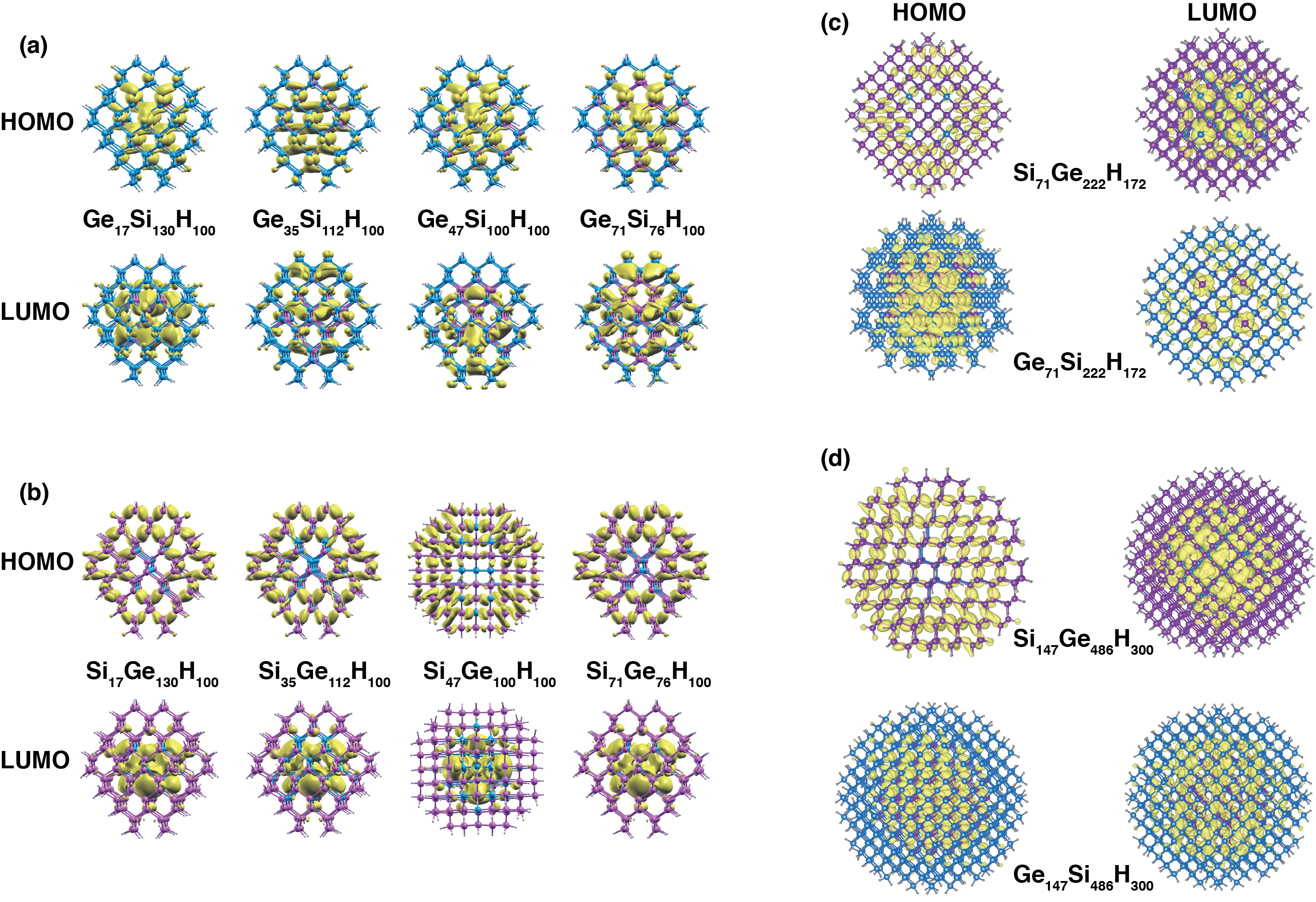
The HOMO and LUMO states localization for Si/Ge and Ge/Si CSNCs of about 1.8 nm of diameter is depicted in Fig. 1, panels (a) and (b). Si(core)/Ge(shell) and Ge(core)/Si(shell) NCs manifestly show a different behavior. As for Si(core)/Ge(shell) NCs, near-valence-edge states (in particular the HOMO state depicted in Fig. 1, panel b) are mainly localized in the shell region, while near-conduction-edge states (and particularly the LUMO state) are mainly localized in the core region, thus leading to the formation of a type II offset. This result is coherent with the discussion presented in Sect. III.1.
Noticeably, this behavior is independent of the CSNCs composition, i.e. on the parameter . On the contrary, in Ge(core)/Si(shell) NCs, both the near-valence and near-conduction-edge states (in particular the HOMO and LUMO states, see Fig. 1 panel a) are mainly localized in the core region, that is on Ge atoms. Hence, in this case, we do not observe the formation of a type II junction, as the offset presents a type I character. Even in this case, the results are independent on the CSNCs composition.
Similar results are obtained for both CSNCs with a diameter of and nm. This is shown in the right panel of Fig. 1, where the HOMO and LUMO states localization is depicted for the Si71Ge222H172 and the Ge71Si222H172 (panel c) and for the Si147Ge486H300 and Ge147Si486H300 (panel d) (for simplicity, we report only the HOMO and LUMO wavefunctions localization for CSNCs with P ). In all these cases, Si(core)/Ge(shell) NCs show a type II offset, while the band-offset character of the Ge(core)/Si(shell) NCs mainly resemble that of a type I heterostructure, with both the HOMO and LUMO states mainly localized on the Ge atoms, in particular the LUMO in the outermost part of the core region, near the Si/Ge interface. This is an important point that will be resumed later.
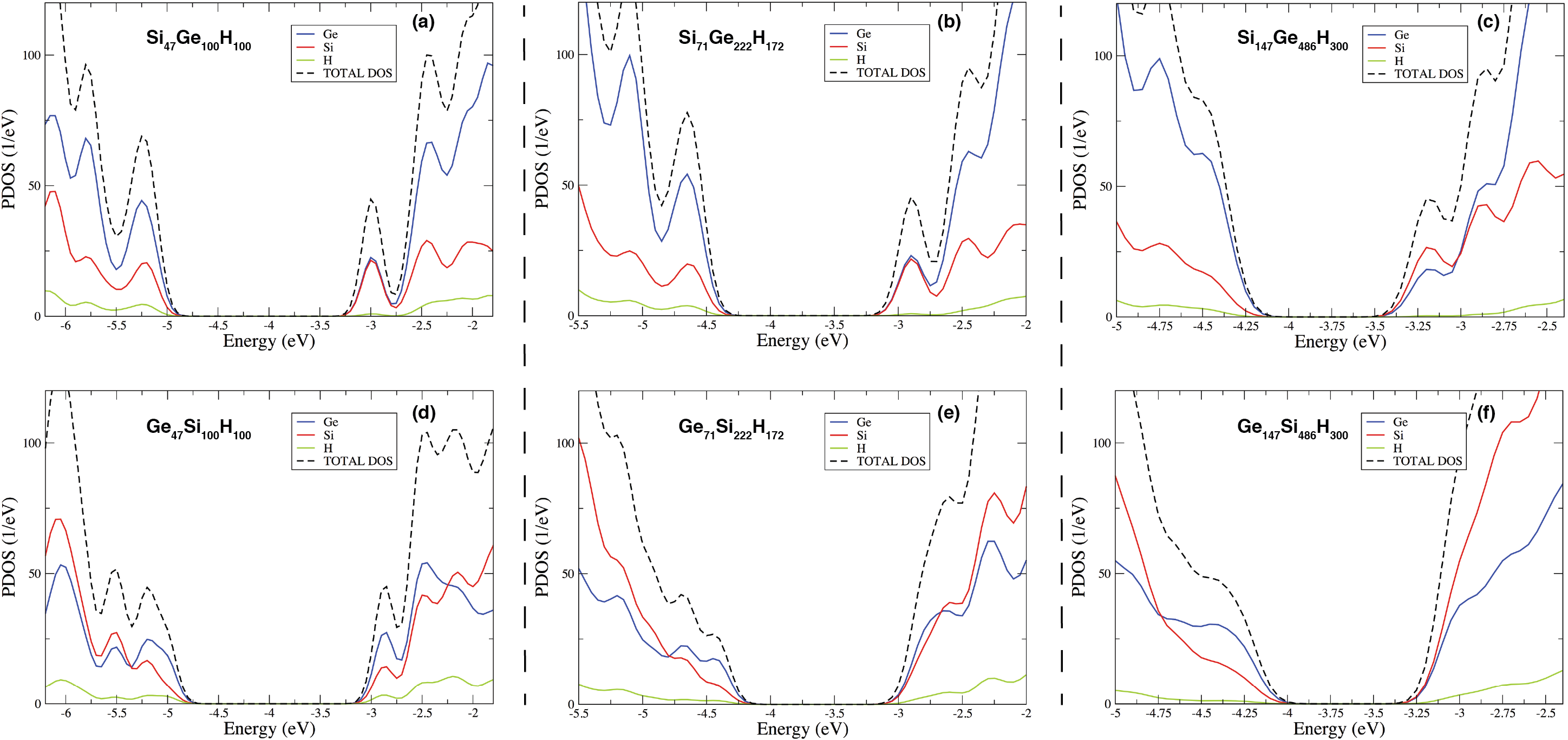
Differences between band-offset characters of Si(core)/Ge(shell) and Ge(core)/Si(shell) NCs emerge also by the results of Fig. 2, where the projected density of states (PDOS) are calculated for the Si47Ge100H100, the Si71Ge222H172, the Si147Ge486H300 (panels a-c, Fig.2) and for the Ge47Si100H100, the Ge71Si222H172 and finally the Ge147Si486H300 (panels d-f, Fig.2). For what concerns the Ge(core)/Si(shell) NCs, in particular, electronic states near both the valence and the conduction band-edges have a clear Ge-like character, which contrasts with the formation of a type II offset. This Ge-like character decreases moving from the smallest to the largest NC, which suggests a reduction of the CBO with increasing NC size. This behaviour is confirmed by the analysis of the spatial localization of the KS unoccupied states. For what concerns the Ge47Si100H100, indeed, the first unoccupied state localized on the Si (LUMOSi) is eV above the first unoccupied state localized on the Ge (LUMOGe), that in this system constitutes the CBM. The CBO is reduced to eV when the Ge71Si222H172 is considered and moves to only eV for the Ge147Si486H300. Therefore, the Ge147Si486H300 still shows a type I offset but, in this system, DFT predicts LUMOGe and LUMOSi states to be almost degenerate energy levels, meaning that Ge(core)/Si(shell) NCs of nm are close to a type I type II band-offset transition. The calculation of wavefunctions localization and of the PDOS are useful to understand band-offset properties of both Si/Ge and Ge/Si CSNCs, but does not allow (i) understanding which mechanisms lead to the formation of a well-defined offset, (ii) defining which parameters differentiate the behavior of the Si(core)/Ge(shell) from that of the Ge(core)/Si(shell), and finally (iii) explaining the trend of the band-offset as the size of the NC (and therefore the core and shell thickness) increases. These points will be addressed in the next sections. Since the main differences between the Si(core)/Ge(shell) and Ge(core)/Si(Shell) are related to the localization of the LUMO state (see Sect. III.1), in the following, we will mainly focus our attention on the CBO properties.
III.3 Si/Ge and Ge/Si core shell NCs: the role of quantum confinement
To obtain a semi-quantitative analysis of the mechanisms influencing the formation of the band-offset, we consider two separated systems obtained from both the CSNCs with a diameter of and nm (). The first ones are generated by extracting the core region from the CSNCs and then capping its surface with hydrogen atoms. The second ones are obtained by extracting the shell region from the CSNCs and, again, passivating with hydrogen all the internal dangling chemical bonds. As a first step, only additional hydrogen positions are relaxed, keeping both Si and Ge atomic positions unaltered, thus preserving the strain induced by the formation of a Si/Ge interface on both the core and the shell regions.
Since in this case the Si/Ge interface is not explicitly taken into account, the adoption of such a model cannot lead to a precise quantitative analysis of the band-offset properties of Si/Ge and Ge/Si CSNCs.
For instance, by impeding the wavefunctions delocalization on both core and shell region, it leads to an overestimation of the confinement of the electronic charge density. However, it is a good approximation to (i) understand if the QCE has a different relevance in the core and shell regions and (ii) clarify the role played by strain or, more generally, by the structural distortions induced by the formation of a Si/Ge interface.
The obtained systems are, on one side, the NCs cores Si71H84c, Ge71H84c, Si147H100c and Ge147H100c (the first two extracted from the CSNCs with nm, the other two from the CSNCs with nm), and, on the other side, the nanostructured shell caps Si222H256s, Ge222H256s, Si486H400s and Ge486H400s (same as above). The subscripts and indicate that the related (nano)structure is obtained by extracting the core or the shell of the NC, respectively.
The structures are then fully relaxed to evaluate the effects induced by strain on the band-offset properties. The obtained unstrained systems are identified with the label relax. We refer to Sect. III.4 for the discussion concerning the role played by strain and we focus here on the connection between the shape of the nanostructures and the QCE, that is on the effects induced by core and shell conformation on the charge density confinement.
To evaluate the effects of QC, we consider structures obtained by extracting the shell region from the CSNCs - i.e. the nanostructured shell caps
Si222H256s, Ge222H256s, Si486H400s and Ge486H400s - and we compare their electronic properties with the ones of H-terminated spherical NCs containing a similar number of Si or Ge atoms - i.e. the Si239H196, the Ge239H196, the Si489H276 and the Ge489H276 NCs.
The goal is to understand how the QCE depends on the shape of the nanostructures, and especially what happens when we move from a spherical nanostructure (e.g. the core of the CSNC) to a nanostructured cap (e.g. the shell of the CSNC) containing the same number of atoms. Noticeably, this kind of analysis will help us clarify if QC is generally more relevant in the core or in the shell region of CSNCs.
After calculating the electronic properties, we analyze the energy level alignment with respect to the vacuum level. The obtained results are reported in Fig. 3.
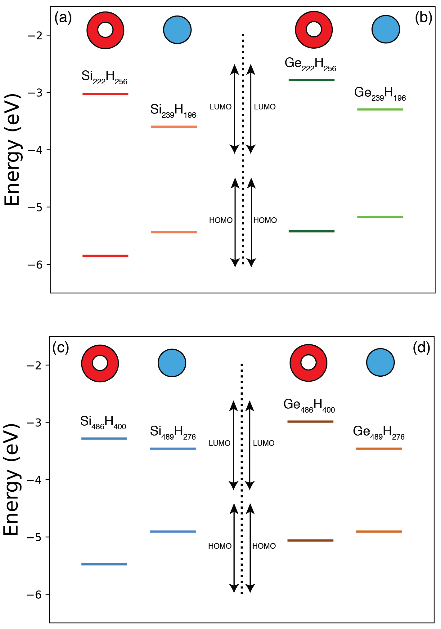
They show that both energy gaps and ionization potential IP (measured as the energy distance between the HOMO and the vacuum level) are larger in the nanostructured shell caps than in the corresponding spherical NCs, while the electronic affinity EA (measured as the energy distance between the LUMO and the vacuum level) is smaller.
For instance, the EA of the Si222H256s
is, in absolute value, eV lower than the one of the Si239H196, while the EA of the Si486H400s is eV lower than the one of the Si489H276. Considering that strain, as we will show later, does not essentially affect the energy of the LUMO, we can safely affirm that the QCE is more pronounced when Si atoms are distributed in a shell cap than inside a sphere. Regarding Ge nanostructures, we find that the calculated EA for the Ge222H256s is, in module, eV lower than the one of the Ge239H196 and that the EA obtained for the Ge486H400s is eV lower than the one of the Ge489H276. Even for Ge, therefore, we can say that the QCE is more pronounced when atoms are distributed in a shell cap than inside a sphere. However, in this case the differences in the calculated EA cannot be ascribed only to the core and shell shape but, as will be later shown, are also affected by strain. Anyway, our conclusions do not change if we repeat the same analysis by considering the fully relaxed shell nanostructures.
The obtained results point out that, for reasons related to the geometry of the system, QC acts differently in the core and in the shell regions of CSNCs. Therefore, the band-offset character of Si/Ge and Ge/Si CSNCs cannot be, in principle, determined by simply considering the band energy alignment of Si and Ge bulks, surfaces or NCs of the same size.
Starting from these findings, we can try to give a preliminar interpretation of the data of Fig. 1, in particular for the Ge(core)/Si(shell) NCs whose band-offset properties deviate from the ones predicted by the IEBA scheme.
In these systems, two different concurrent effects contribute to the formation of the band-offset, and in particular they influence the energy levels alignment of the unoccupied states. The first effect, already discussed in Sect. III.1, implies that, in similar Si and Ge nanostructures, QC acts more markedly on the LUMO than on the LUMO. In low-dimensional systems, therefore, the LUMO is shifted toward higher energies, that is, it tends to get closer to the vacuum level. This effect would strengthen the intrinsic type II offset that generally characterizes Si/Ge junctions.
On the other hand, the electronic charge confinement is generally larger in the shell than in the core region, as shown in Fig.3.
This effect is in competition with the one mentioned above and moves the LUMO to higher energies (that is, energies closer to the vacuum level) than the LUMO.
Despite the Ge(core)/Si(shell) NCs of Fig. 1 have , the second effects cannot be neglected (also because these CSNCs show a thin shell region, approximately less than nm), fostering the formation of a type I offset.
Obviously, the larger the shell, the weaker QC is in this region.
The two aforementioned effects are instead combined to enhance the shift of the LUMO toward higher energies when the Si(core)/Ge(shell) NCs are considered. In this case, the different relevance of the QCE in the core and shell regions strengthens the formation of a type II offset. The quantum confinement of the electronic charge induced by both core and shell morphology is not, however, the only parameter we have to consider. A fundamental role is also played by strain, especially when small CSNCs are considered. Effects induced by strain on the band-offset properties of the considered systems will be discussed in the next section.
III.4 SiGe and GeSi core shell NCs: the role of strain
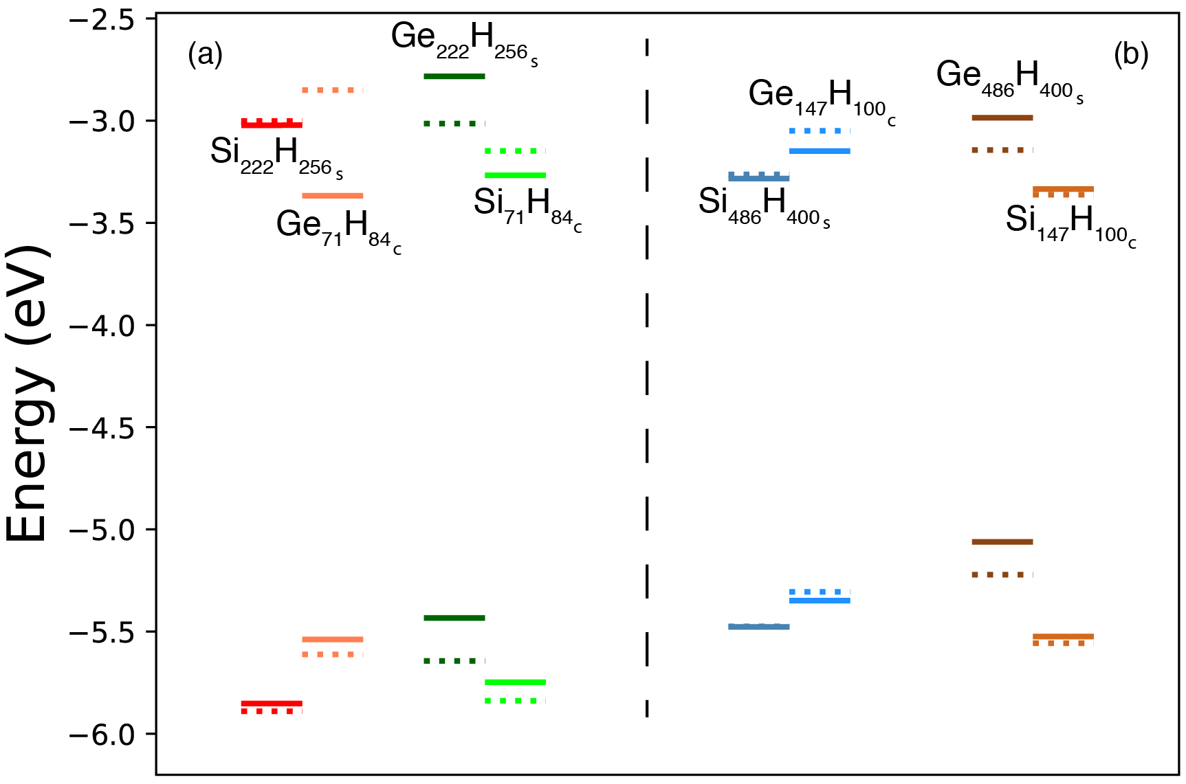
In order to investigate the effects generated on the electronic properties by strain, we focus our attention on the core and shell structures extracted from the CSNCs. These systems can be analyzed to separate and understand the role played by both QC and strain. In Fig. 4, solid lines of the panel (a), we report the energy levels alignment calculated for the LUMO and HOMO states for the structures extracted from the CSNCs with a diameter of nm. The band diagram is thus obtained for the Si222H256s and the Ge71H84c, that is the systems extracted from the nm Ge/Si CSNC, and for the Ge222H256s and the Si71H84c (obtained starting from the nm Si/Ge CSNC). In panel (b) the same analysis is performed for the nanostructures extracted from the CSNCs with a diameter of nm. In both panels (a) and (b), dotted lines refer to the fully relaxed structures.
A comparison between solid and dotted lines will help to clarify the role played by strain, as it will be discussed later. First, we focus our attention on the results identified by solid lines, in order to discuss the accuracy of a model based on the study of the core and shell regions taken separately.
Initially, we note that the band-offsets derived from the energy levels alignment of panel (a) are in agreement with the outcomes of Fig. 1 panel (c), that is a type II offset for the systems extracted from the Si(core)/Ge(shell) NCs and a type I offset for the structures generated from the Ge(core)/Si(shell) NCs. The CBO obtained by the energy levels alignment of the Si222H256s and the Ge71H84c (Ge222H256s and Si71H84c) is eV ( eV), a value that approaches the one obtained for the corresponding Ge/Si (Si/Ge) CSNC, that is eV ( eV). These results point out a discrepancy of about eV between the CBO obtained from the results of Fig. 4 and the ones corresponding to the structures of Fig. 1, panel (c).
We now move on to consider the results reported in panel (b) of Fig. 4.
The energy level alignment of the systems extracted from the nm Si(core)/Ge(shell) NC (that is the Ge486H400 and the Si147H100), presents a type II character, in agreement with the results of Fig. 1, panel d. Regarding the nm Ge(core)/Si(shell) NC, instead, the model applied in Fig. 4 fails to predict a type I offset, by moving up
the crossing between the LUMO and the LUMO levels, and thus the transition from the type I to the type II offset. This result is not surprising because, as underlined before, a model based on the energy levels alignment of structures extracted from CSNCs cannot exactly define neither the CBO nor the LUMO-LUMO crossing point. Therefore it cannot accurately predict at which diameter the type I type II transition occurs. As a good approximation, however, it can indicate if we are close to observing such a transition.
Noticeably, the type I offset calculated for the whole Ge147Si486H300 shows a CBO of only eV, that is the LUMO and the LUMO are almost degenerate, while the HOMO - LUMO energy alignment obtained for the separated Si486H400s and Ge147H100c partes point out a type II offset with a CBO of only eV, a result that confirms the accuracy of the method with an error in the estimation of the band offset properties of about eV. Starting from these considerations, we compare the solid and dotted lines of Fig. 4. As a result, we can observe that distortions induced by the formation of a Si/Ge interface mainly affect the band-offset properties of the smaller structures, that is the ones reported in panel (a), which refer to the CSNCs with a diameter of nm and, above all, they impact on the energy of the LUMOGe state.
In particular, by focusing on the results reported in panel (a) of Fig. 4, we observe an increase of about eV of the LUMO energy when we move from the Ge71H84c (solid orange line) to the Ge71H (dotted orange line) and a lowering of
eV of the energy of the LUMO level when we move from the Ge222H256s to the Ge222H (from solid to dotted green lines of panel a). As a consequence, structural distortions induced by the formation of a Si/Ge interface strengthen the type I offset in the nm Ge(core)/Si(shell) NC and the type II offset in the nm Si(core)/Ge(shell) NC. In order to understand these changes, we have to remember that, as a consequence of strain, in both the Si(core)/Ge(shell) and the Ge(core)/Si(shell) NCs, the LUMOGe state is mainly localized in the proximity of the Si/Ge interface. This characteristic is also present in the isolated core and shell nanostructures. In particular, the LUMOGe is localized in the outermost part (that is, near the surface) of the Ge71H84c and in the proximity of the internal surface when the nanostructured spherical cap Ge222H256s is taken into account. When systems are fully relaxed, and the distortions induced by the formation of a Si/Ge interface are removed, the LUMOGe state appears to be more localized in the central part of the nanostructures. This implies a more pronounced confinement of the LUMOGe state in the structure extracted from the core, with a consequent shift to higher energies of the LUMOGe when strain is removed (from solid to dotted orange lines). At the same time, a weaker confinement of the LUMOGe state in the structure extracted from the shell, with a consequent reduction of the LUMOGe energy (from solid to dotted green lines) is found.
The same trends can be observed for the Ge structures of panel (b) but, in this case, due to the larger size of the systems, the effects induced by strain are less relevant. Regarding Si nanostructures, we do not observe drastic changes in the HOMO and LUMO positions when strain is removed (changes are always less than eV), confirming that Si NCs are less sensitive to the strain than Ge ones [81].
The results of Fig.4 clarify that a second condition has to be verified in order to observe a type II offset in the Ge(core)/Si(shell) NCs, that is, the core has to be sufficiently large to reduce the effects induced by strain. When this last condition is not verified, structural distortions present in the core region (induced by the Si and Ge lattice mismatch) induce a lowering of the LUMOGe energy, strengthening the type I offset.
As a consequence, starting from the nm Ge147Si486H300 NC, which shows a type I offset, we cannot obtain a type II heterostructure by simply increasing the shell thickness while keeping the size of the NC constant. By doing so, indeed, we also reduce the core extension, thus increasing the relevance of strain in this region. The result would be a simultaneous lowering of both the LUMOSi and LUMOGe energies, the former induced by the slight reduction of the QCE in the shell region, the latter by increasing strain in the core region, which would not produce changes in the band-offset character. To verify this point, we have performed calculations considering the nm Ge71Si562H300 (core diameter of about nm, shell thickness of about nm) still obtaining a type I offset with a CBO even increased to eV.
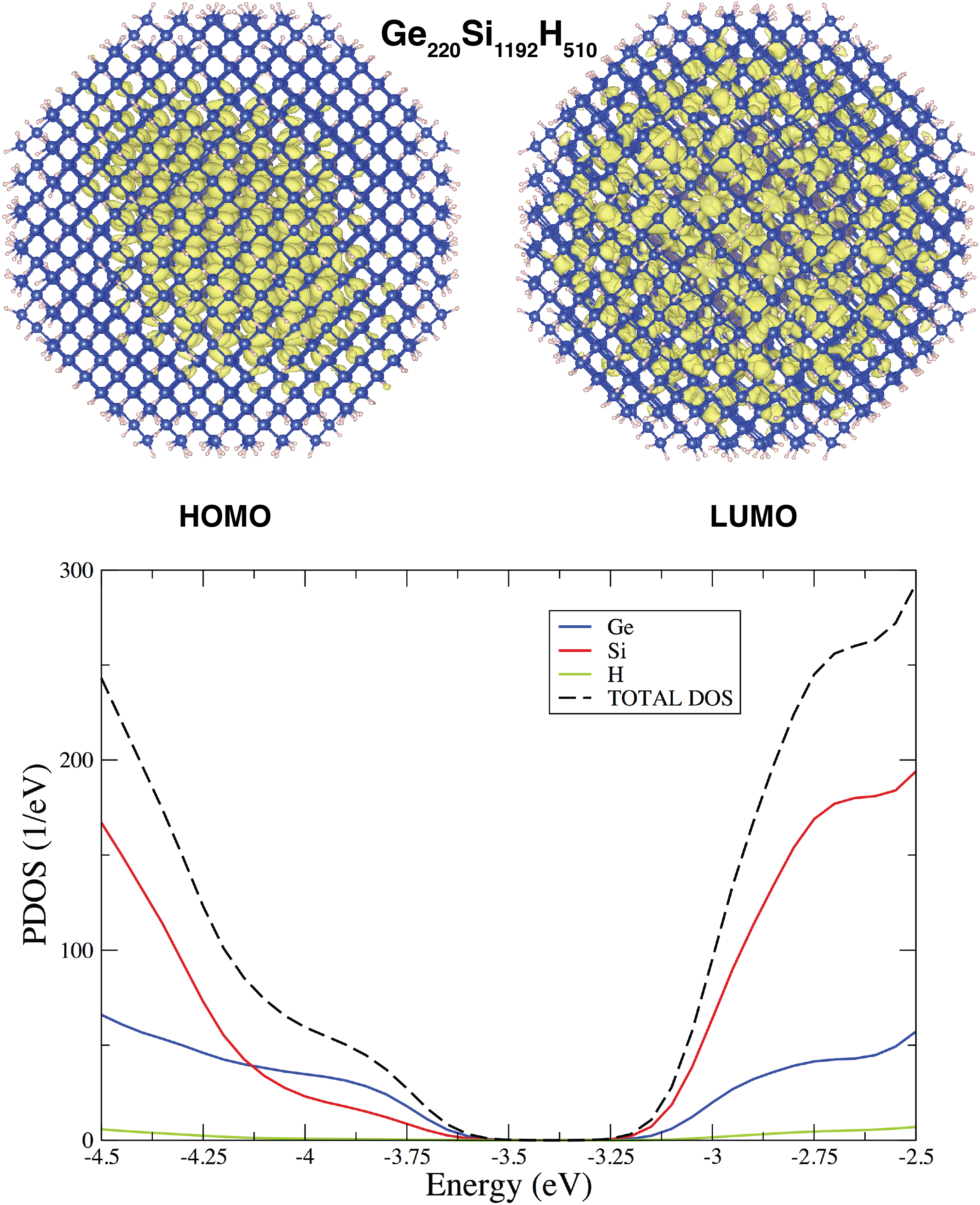
The diameter nm represents therefore a sort of critical size for the Ge(core)/Si(shell) NCs. Below this threshold, we clearly observe a type I offset with both the HOMO and LUMO states mainly localized on the Ge atoms; the same offset is observed for Ge(core)/Si(shell) NCs with a diameter of about nm, but in this case we are in proximity of the type I type II transition. Finally, a type II offset can result for Ge(core)/Si(shell) NCs with nm. This condition guarantees the possibility of obtaining CSNCs with, at the same time, a sufficiently large shell to reduce the QCE in the Si region, and a sufficiently large core to reduce the effects induced by strain in the Ge region. As an example, we report in Fig. 5 the case concerning the
Ge220Si1192H510 ( nm, nm) which shows a type II band-offset, with the HOMO mainly localized in the core around the Ge atoms, and the LUMO localized on the Si atoms, thus outside of the core region, in between the Si/Ge interface and the outermost part of the shell. The formation of a type II band-offset is also confirmed by the calculated PDOS, as reported in Fig. 5 bottom panel.
IV Conclusions
In this paper, Density Functional Theory has been adopted in order to investigate the mechanisms involved in the formation of the band-offset of Si/Ge and Ge/Si CSNCs, and in particular to discern the role played by the QCE and strain. NCs with diameters ranging from to nm have been considered. This analysis is crucial because, depending on the band-offset character - type I or type II -, NCs are more suitable to be engineered in light-emitting (type I) or in photovoltaic (type II) devices. Our results point out that both QC and strain contribute to the formation of type II offset in Si(core)/Ge(shell), with the HOMO localized in the Ge shell and the LUMO localized in the Si core. In these systems, therefore, the band-edge properties resemble those obtained by simply considering the intrinsic properties of the Si and Ge materials. The analysis is far more subtle for Ge(core)/Si(shell) NCs. In these NCs the HOMO state is always localized in the core region while the LUMO localization depends on the geometry of the system, which determines the relevance of QC and strain on both core and shell regions. Our calculations point out that QC is generally more pronounced in the shell than in the core region. In Ge(core)/Si(shell) NCs, indeed, the QC contributes to moving the LUMOSi level to higher energies. On the contrary, the strain induced by the formation of a Si/Ge interface mainly affects the LUMOGe state, lowering its energy. As a result, in Ge/Si CSNCs with a diameter less than nm, the LUMO is always localized on the Ge inducing a type I offset. Our outcomes point out that, depending on the band-offset properties, spherical GeSi CSNCs can be grouped into three different classes. CSNCs with a diameter less than nm are clearly characterized by a type I offset. CSNCs with a diameter of about nm still show a type I offset though they have the critical size for observing a type I type II transition. Finally, CSNCs with diameters above nm can present a type II offset because, in this case, core and a shell are sufficiently large to reduce the effects induced by strain in the internal core region, and by the QCE, in the external shell. This has been directly demonstrated in the case of a large Ge220Si1192H510 CSNC, where calculations reveal indeed a type II band-offset.
V Appendix
| diameter (nm) | Ge(core)/Si(shell) | Energy Gap (eV) | Si(core)/Ge(shell) | Energy Gap (eV) |
| 1.8 | Ge17Si130H100 | 2.09 | Si17Ge130H100 | 2.10 |
| 1.8 | Ge35Si122H100 | 2.12 | Si35Ge122H100 | 2.12 |
| 1.8 | Ge47Si100H100 | 2.11 | Si47Ge100H100 | 2.12 |
| 1.8 | Ge71Si76H100 | 2.16 | Si71Ge76H100 | 2.10 |
| 2.4 | Ge71Si222H1772 | 1.54 | Si71Ge222H172 | 1.67 |
| 3.0 | Ge147Si486H300 | 1.19 | Si147Ge486H300 | 1.19 |
| 3.0 | Ge71Si562H300 | 1.17 | - | - |
| 4.0 | Ge220Si1192H510 | 0.83 | - | - |
In this section, we report additional information concerning electronic and optical properties of the systems analysed in the manuscript.
Calculated LDA energy gaps are reported in Table 1. It is evident that the depend only marginally on the CSNCs composition and, following the typical trend imposed by the QCE, decrease when the NCs size increases. Moreover, by focusing on the smaller NCs, we can also observe that the calculated for the CSNCs do not strongly differ from those of the pristine Si147H100 and Ge147H100 NCs.
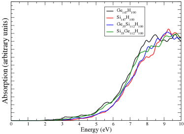
For the smaller nanocrystals, we have also calculated the absorption spectra using the Liouville–Lanczos approach to Time-Dependent Density Functional Perturbation Theory, as implemented in the TDDFT tool of the QE package [82]. The results obtained for the pristine Si147H100 and Ge147H100 NCs and the Ge35Si122H100 and the Si35Ge122H100 CSNCs are depicted in Fig. 6.
The spectra calculated for the CSNCs, and their absorption energy thresholds, fall in-between the ones obtained for the Si147H100 and the Ge147H100 NCs.
In Table 1, we also report the GW gap of one of the smallest NCs, i.e. Ge35Si122H100. Quasi-particle calculations were introduced in order to check if a different energy levels alignment could arise when many-body effects are taken into account. Convergence tests are shown in Fig.7. GW corrections are sizeable, opening the DFT gap by about 1.4 eV; nevertheless, no change in the band-edge ordering is observed. In both DFT and GW, the states around the gap are mainly localized on the Ge core, hence giving a type I heterostructure. The first unoccupied state mainly localized on Si is at 0.29 eV above the LUMO in DFT (0.2 eV above the LUMO in GW); analogously, the first occupied Si state is located 0.46 eV below the HOMO (1.0 eV below the HOMO in GW). Hence, the DFT alignment is confirmed also by quasi-particle calculations.

VI Acknowledgments
I.M., S.G., O.P. and S. O. thank the Super-Computing Interuniversity Consortium CINECA for support and high-performance computing resources under the Italian Super-Computing Resource Allocation (ISCRA) initiative, and under PRACE. S.O. acknowledges support/funding from University of Modena and Reggio Emilia under project ”FAR2017INTERDISC”. O.P. and S.G. acknowledge financial funding from the EU MSCA-RISE project DiSeTCom (GA 823728) and INFN project TIME2QUEST. Technical support by Dr. Ihor Kupchak is gratefully acknowledged. M.A. greatly acknowledges the ANR AMPHORE project (ANR-21-CE09-0007) of the French Agence Nationale de la Recherche.
References
- [1] M. V. Wolkin, J. Jorne, P. M. Fauchet, G. Allan, and C. Delerue, Phys. Rev. Lett. 82, 197 (1999).
- [2] L. Pavesi, C. Dal Negro, L. Mazzoleni, G. Franzó, and F. Priolo, Nature 408, 440 (2000).
- [3] D. V. Melnikov and J. R. Chelikowsky, Phys. Rev. B 69, 113305 (2004).
- [4] Y. Nakamura, A. Masada, and M. Ichikawa, Applied Physics Letters 91, 013109 (2007).
- [5] M. Scarselli, S. Masala, P. Castrucci, M. De Crescenzi, E. Gatto, M. Venanzi, A. Karmous, P. D. Szkutnik, A. Ronda, and I. Berbezier, Applied Physics Letters 91, 141117 (2007).
- [6] M. Govoni, I. Marri, and S. Ossicini, Nat. Photon. 6, 672 (2012).
- [7] I. Marri, M. Govoni, and S. Ossicini, Journal of the American Chemical Society 136, 13257 (2014), PMID: 25092549.
- [8] I. Marri, M. Govoni, and S. Ossicini, Beilstein Journal of Nanotechnology 6, 343 (2015).
- [9] F. Priolo, T. Gregorkiewicz, M. Galli, and T. F. Krauss, Nature Nanotechnology 9, 19 (2014).
- [10] M. Vörös, S. Wippermann, B. Somogyi, A. Gali, D. Rocca, G. Galli, and G. T. Zimanyi, J. Mater. Chem. A 2, 9820 (2014).
- [11] I. Marri, M. Govoni, and S. Ossicini, Solar Energy Materials and Solar Cells 145, 162 (2016), Selected papers of the EMRS 2015 Spring meeting – Symposium C on Advanced Inorganic Materials and Structures for Photovoltaics.
- [12] I. Marri, E. Degoli, and S. Ossicini, Progress in Surface Science 92, 375 (2017).
- [13] M. V. Kovalenko, L. Manna, A. Cabot, Z. Hens, D. V. Talapin, C. R. Kagan, V. I. Klimov, A. L. Rogach, P. Reiss, D. J. Milliron, P. Guyot-Sionnnest, G. Konstantatos, W. J. Parak, T. Hyeon, B. A. Korgel, C. B. Murray, and W. Heiss, ACS Nano 9, 1012 (2015).
- [14] E. Degoli, R. Guerra, F. Iori, R. Magri, I. Marri, O. Pulci, O. Bisi, and S. Ossicini, Comptes Rendus Physique 10, 575 – 586 (2009), Cited by: 24.
- [15] A. Angı, R. Sinelnikov, A. Meldrum, J. G. C. Veinot, I. Balberg, D. Azulay, O. Millo, and B. Rieger, Nanoscale 8, 7849 (2016).
- [16] M. Dutta, L. Thirugnanam, P. V. Trinh, and N. Fukata, ACS Nano 9, 6891 (2015).
- [17] R. Sinelnikov, M. Dasog, J. Beamish, A. Meldrum, and J. G. C. Veinot, ACS Photonics 4, 1920 (2017).
- [18] I. Fraj, L. Favre, T. David, M. Abbarchi, K. Liu, J. Claude, A. Ronda, M. Naffouti, F. Saidi, F. Hassen, H. Maaref, J. Aqua, and I. Berbezier, Applied Surface Science 419, 476 (2017).
- [19] C. Delerue, Phys. Rev. B 98, 045434 (2018).
- [20] I. Marri, E. Degoli, and S. Ossicini, physica status solidi (a) 215, 1700414 (2018).
- [21] M. Tkalčević, L. Basioli, K. Salamon, I. Šarić, J. S. Parramon, M. Bubaš, I. Bogdanović-Radović, S. Bernstorff, Z. Fogarassy, K. Balázsi, M. Petravić, and M. Mičetić, Solar Energy Materials and Solar Cells 218, 110722 (2020).
- [22] I. Marri, M. Amato, M. Bertocchi, A. Ferretti, D. Varsano, and S. Ossicini, Phys. Chem. Chem. Phys. 22, 25593 (2020).
- [23] V. Dhyani, G. Ahmad, N. Kumar, and S. Das, IEEE Transactions on Electron Devices 67, 558 (2020).
- [24] L. Basioli, J. Sancho-Parramon, V. Despoja, S. Fazinić, I. Bogdanović Radović, I. Božićević Mihalić, K. Salamon, N. Nekić, M. Ivanda, G. Dražić, S. Bernstorff, G. Aquilanti, and M. Mičetić, ACS Applied Nano Materials 3, 8640 (2020).
- [25] L. Pavesi, Frontiers in Physics 9, 786028 (2021).
- [26] I. Marri and S. Ossicini, Nanoscale 13, 12119 (2021).
- [27] D. J. Paul, Semicond. Sci. Technol. 19, R75 (2004).
- [28] M. L. Lee, E. A. Fitzgerald, M. T. Bulsara, M. T. Currie, and A. Lochtefeld, J. Appl. Phys. 97, 011101 (2005).
- [29] Y. J. Ma, Z. Zhong, Q. Lv, T. Zhou, X. J. Yang, Y. L. Fan, Y. Q. Wu, J. Zou, and Z. M. Jiang, Applied Physics Letters 100, 153113 (2012).
- [30] S.-W. Lee, H.-T. Chang, J.-K. Chang, and S.-L. Cheng, Journal of The Electrochemical Society 158, H1113 (2011).
- [31] A. Alkhatib and A. Nayfeh, Scientific Reports 3, 2099 (2013).
- [32] M. Buljan, S. R. C. Pinto, A. G. Rolo, J. Martín-Sánchez, M. J. M. Gomes, J. Grenzer, A. Mücklich, S. Bernstorff, and V. Holý, Phys. Rev. B 82, 235407 (2010).
- [33] J. Yang, Y. Jin, C. Wang, L. Li, D. Tao, and Y. Yang, Applied Surface Science 258, 3637 (2012).
- [34] N. Nekic, J. Sancho-Parramon, I. Bogdanovic-Radovic, J. Grenzer, R. Hübner, S. Bernstorff, M. Ivanda, and M. Buljan, Nanophotonics 6, 1055 (2017).
- [35] I. Stavarache, C. Logofatu, M. T. Sultan, A. Manolescu, H. G. Svavarsson, V. S. Teodorescu, and M. L. Ciurea, Scientific Reports 10, 3252 (2020).
- [36] B. Li, J. Liu, G. F. Liu, and J. A. Yarmoff, Applied Physics Letters 91, 132107 (2007).
- [37] H.-K. Chang and S.-C. Lee, Applied Physics Letters 97, 251912 (2010).
- [38] C.-S. Yang, S. M. Kauzlarich, and Y. C. Wang, Chemistry of Materials 11, 3666 (1999).
- [39] C. Mehringer, C. Kloner, B. Butz, B. Winter, E. Spiecker, and W. Peukert, Nanoscale 7, 5186 (2015).
- [40] K. I. Hunter, J. T. Held, K. A. Mkhoyan, and U. R. Kortshagen, Acs Applied Materials & Interfaces 9, 8263 (2017).
- [41] Uddin, Md. Seraj, Vijayan, C., and Rath, Jatindra Kumar, Eur. Phys. J. Appl. Phys. 91, 20801 (2020).
- [42] K. Mori, K. Shoda, and H. Kohno, Applied Physics Letters 87, 083111 (2005).
- [43] J. Xiang, W. Lu, Y. Hu, Y. Wu, H. Yan, and C. M. Lieber, Nature 441, 489 (2006).
- [44] G. Liang, J. Xiang, N. Kharche, G. Klimeck, C. M. Lieber, and M. Lundstrom, Nano Letters 7, 642 (2007).
- [45] P. M. Mooney and J. O. Chu, Annual Review of Materials Science 30, 335 (2000).
- [46] H. Rucker and B. Heinemann, Semiconductor Science and Technology 33, 114003 (2018).
- [47] S. Shi, A. Zaslavsky, and D. Pacifici, Applied Physics Letters 117, 251105 (2020).
- [48] C. Palade, I. Stavarache, T. Stoica, and M. L. Ciurea, Sensors 20, 6395 (2020).
- [49] Y. Li, C. Cui, J. Song, Q. Liu, S. Yuan, C. Zeng, and J. Xia, Nanotechnology 31, 385603 (2020).
- [50] D. M. Zhigunov, A. B. Evlyukhin, A. S. Shalin, U. Zywietz, and B. N. Chichkov, ACS Photonics 5, 977 (2018).
- [51] X. Zhao, D. Li, T. Zhang, B. Conrad, L. Wang, A. H. Soeriyadi, J. Han, M. Diaz, A. Lochtefeld, A. Gerger, I. Perez-Wurfl, and A. Barnett, Solar Energy Materials and Solar Cells 159, 86 (2017).
- [52] R. Lachaume, M. Foldyna, G. Hamon, J. Decobert, R. Cariou, P. Roca i Cabarrocas, J. Alvarez, and J. Kleider, Solar Energy Materials and Solar Cells 166, 276 (2017).
- [53] H. Liu, W. Winkenwerder, Y. Liu, D. Ferrer, D. Shahrjerdi, S. K. Stanley, J. C. Ekerdt, and S. K. Banerjee, IEEE Trans. Electr. DEv. 55, 3610 (2008).
- [54] S. Yamasaka, K. Watanabe, S. Sakane, S. Takeuchi, A. Sakai, K. Sawano, and Y. Nakamura, Sci. Rep. 6, 22838 (2016).
- [55] M. Amato, M. Palummo, R. Rurali, and S. Ossicini, Chem. Rev. 114, 1371 (2014).
- [56] N. Fukata, M. Yu, W. Jevasuwan, T. Takei, Y. Bando, W. Wu, and Z. L. Wang, ACS Nano 9, 12182 (2015).
- [57] X. Zhang, W. Jevasuwan, K. C. Pradel, T. Subramani, T. Takei, and N. Fukata, Nanoscale 10, 21062 (2018).
- [58] X. Zhang, W. Jevasuwan, and N. Fukata, Nanoscale 12, 7572 (2020).
- [59] X. D. Pi and U. R. Kortshagen, Nanotechnology 20, 295602 (2009).
- [60] I. Berbezier and A. Ronda, Surface Sci. Rep. 64, 47 (2009).
- [61] J.-N. Aqua, I. Berbezier, L. Favre, T. Frisch, and A. Ronda, Phys. Rep. 522, 52 (2013).
- [62] L. E. Ramos, J. Furthmüller, and F. Bechstedt, Phys. Rev. B 72, 045351 (2005).
- [63] M. B. Javan, Thin Solid Films 589, 120 (2015).
- [64] O. Cojocaru, A.-M. Lepadatu, G. A. Nemnes, T. Stoica, and M. L. Ciurea, Scientific Reports 11, 13582 (2021).
- [65] T. Tayakagi, Y. Hoshi, and N. Usami, Sci. Rep. 3, 2703 (2013).
- [66] E. L. de Oliveira, E. L. Albuquerque, J. S. de Sousa, G. A. Frarias, and F. M. Peeters, J. Phys. Chem. C 116, 4399 (2012).
- [67] M. O. Nestoklon, A. N. Poddubny, P. Voisin, and K. Dohnalova, J. Phys. Chem. C 120, 18901 (2016).
- [68] M. R. Neupane, R. K. Lake, and R. Rahman, J. Appl. Phys. 110, 074306 (2011).
- [69] M. R.Neupane, R. K. Lake, and R. Rahman, J. Appl. Phys. 112, 024326 (2012).
- [70] M. R. Neupane, R. Rahman, and R. K. Lake, Phys. Chem. Chem. Phys. 17, 2484 (2015).
- [71] P. Giannozzi, S. Baroni, N. Bonini, M. Calandra, R. Car, C. Cavazzoni, D. Ceresoli, G. L. Chiarotti, M. Cococcioni, I. Dabo, A. D. Corso, S. de Gironcoli, S. Fabris, G. Fratesi, R. Gebauer, U. Gerstmann, C. Gougoussis, A. Kokalj, M. Lazzeri, L. Martin-Samos, N. Marzari, F. Mauri, R. Mazzarello, S. Paolini, A. Pasquarello, L. Paulatto, C. Sbraccia, S. Scandolo, G. Sclauzero, A. P. Seitsonen, A. Smogunov, P. Umari, and R. M. Wentzcovitch, J. Phys. Condens. Matter 21, 395502 (2009).
- [72] P. Giannozzi, O. Andreussi, T. Brumme, O. Bunau, M. B. Nardelli, M. Calandra, R. Car, C. Cavazzoni, D. Ceresoli, M. Cococcioni, N. Colonna, I. Carnimeo, A. D. Corso, S. de Gironcoli, P. Delugas, R. A. DiStasio, A. Ferretti, A. Floris, G. Fratesi, G. Fugallo, R. Gebauer, U. Gerstmann, F. Giustino, T. Gorni, J. Jia, M. Kawamura, H.-Y. Ko, A. Kokalj, E. Küçükbenli, M. Lazzeri, M. Marsili, N. Marzari, F. Mauri, N. L. Nguyen, H.-V. Nguyen, A. O. de-la Roza, L. Paulatto, S. Poncé, D. Rocca, R. Sabatini, B. Santra, M. Schlipf, A. P. Seitsonen, A. Smogunov, I. Timrov, T. Thonhauser, P. Umari, N. Vast, X. Wu, and S. Baroni, J. Phys. Condens. Matter 29, 465901 (2017).
- [73] A. Nduwimana, R. N. Musin, A. M. Smith, and X.-Q. Wang, Nano Lett. 8, 3341 – 3344 (2008).
- [74] See www.etsf.eu for the GW code CHISIG developed within the ETSF.
- [75] C. Bostedt, T. van Buuren, T. M. Willey, N. Franco, L. J. Terminello, C. Heske, and T. Möller, Applied Physics Letters 84, 4056 (2004).
- [76] M. Amato, M. Palummo, and S. Ossicini, Phys. Rev. B 79, 201302 (2009).
- [77] T. van Buuren, L. N. Dinh, L. L. Chase, W. J. Siekhaus, and L. J. Terminello, Phys. Rev. Lett. 80, 3803 (1998).
- [78] C. Ruß, K. Zahn, and H.-H. von Grünberg, Journal of Physics: Condensed Matter 15, S3509 (2003).
- [79] F. A. Reboredo, A. Franceschetti, and A. Zunger, Phys. Rev. B 61, 13073 (2000).
- [80] S. P. Beckman, J. Han, and J. R. Chelikowsky, Phys. Rev. B 74, 165314 (2006).
- [81] H.-C. Weissker, J. Furthmüller, and F. Bechstedt, Phys. Rev. B 67, 245304 (2003).
- [82] O. B. Malcıoğlu, R. Gebauer, D. Rocca, and S. Baroni, Computer Physics Communications 182, 1744 (2011).