2022
[1,2]\fnmTomohito \surOtobe
[1]\orgdivKPSI, \orgnameNational Institutes for Quantum Science and Technology, \orgaddress\street8-1-7, Umemidai, \cityKizugawa, \postcode619-0125, \stateKyoto, \countryJapan 2]\orgdivPhoton Science Center, \orgnameThe University of Tokyo, \orgaddress\street7-3-1, Hongo, \cityBunkyo-ku, \postcode111-8656, \stateTokyo, \countryJapan
Effect of the interference in overlapped double-pulse irradiation at the silicon surface
Abstract
We studied the excitation process of silicon under an intense double pulse. We employed the three-temperature (electron, hole, and lattice) model (3TM) together with Maxwell’s equations. We solved Maxwell’s equations by the finite-difference time-domain approach. The lattice temperature and absorbed energy at the surface increase significantly when the two laser pulses overlap with constructive interference. On the other hand, destructive interference reduces the efficiency of laser excitation significantly. On an average, the overlapped double pulse increases the efficiency to about twice of the distinct two-pulse case.
keywords:
laser processing, three-temperature model, double pulse, FDTD1 Introduction
In the recent years, we have been able to use intense laser pulses of duration ranging from femto- to pico-second time scales to investigate laser-matter interaction. In particular, laser processing of semiconductors using ultrashort pulses attracts great interest, due to its application in nano-structuring (Gattass2008, ; Stoian-2020, ). Ultrafast laser pulse enables precise processing of the material, without causing damage in the surrounding area (Sugioka2014, ). There are two approaches to study the laser processing, single-shot and multi-shot.
The single-shot experiment is suitable to study excitation process during the laser pulseKumada-2014 ; Kumada-2016 ; Dinh-2019 , while the multi-shot experiments can study how to control the efficiency of laser processingNakamura-2020 ; Otobe-2017 . In the multi-shot experiment, a pulse-train with distinct laser pulses is employed. Recently, enhancement of laser ablation and processing by an overlapped double-pulse irradiation has been reported Zhang_2015 ; Zhang_2019 ; Wang-2020 .
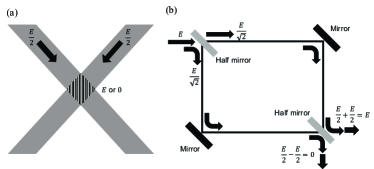
When the two pulses are overlapped, the interference between them plays a crucial role as shown in Fig. 1. If the two pulses with same irradiance () overlap perfectly, constructive interference makes 4-times intense laser field (), while the destructive interference makes a zero intensity regionDrosd-2014 . In the case of non-collinear configuration (Fig. 1(a)), position-dependent intensity distribution occurs. The collinear configuration (Fig. 1(b)) makes constructive and destruction pulse after the second half mirror. Since the laser intensity at the target depends on the relative phase of two pulses, overlapped double-pulse experiments have been done between and intensity, we should take into account the effect of interference.
Some theoretical approaches have been proposed as the extension of two-temperature-model (TTM)Anisimov1974 ; Chen-2005 ; Silaeva_2012 . Recently, we have developed a new numerical model including the time-evolution of electron, hole, and lattice temperatures (3 temperature model=3TM), for the laser excitation process of the silicon Prachi-2022 . One of the features of 3TM is the direct treatment of electromagnetic field (EM-field) with finite-difference time-domain (FDTD) method. In the previous work, we have reported that the 3TM-FDTD reproduces the pulse-duration dependence of the damage threshold of silicon not only qualitatively but also quantitatively.
This paper is organized as follows: Section 2 describes the analytical formulation of 3TM and numerical method for FDTD method, section 3 presents results of excitation in silicon for different delay time of the two pulses and laser intensity, and then finally, we would like to summarize the work in section 4.
2 Formulation
2.1 3TM
The time-evolution of electron and hole densities, and is described as:
| (1) |
where is the laser frequency and is the single photon absorption coefficient for transition from VB to CB (Green2008, ). is the two-photon absorption coefficient for which we use the interpolation of the DFT calculation when Murayama-1995 , where is the optical gap, and we employ the model described in Ref.Garcia_2006 ; Furey-2021 for . is the Auger re-combination coefficient (Silaeva_2012, ) and is the impact ionization coefficient (Chen-2005, ). Equation (2.1) also includes the effect of spatial charge distribution and the associated electric field, and and are the charge current,
| (2) |
diffusion coefficient
| (3) |
and the electric field induced by the electron–hole separation Silaeva_2012 , respectively. Here is the reduced Fermi level:
| (4) |
| (5) |
and
| (6) |
where is the Fermi integral given by
| (7) |
are used depending on whether is positive FUKUSHIMA2015802 or negative Cloutman-1989 .
The total dielectric function along with the effect of band structure re-normalization (Sokol-2000, ) is expressed by
| (8) |
where is the density of valence electrons. It should be noted that and are nearly the same due to the effect of and can be approximated at . is the innate dielectric function, represents the band re-normalization by carrier density, and is the complex dielectric function calculated from Drude model. The temperature dependent optical parameters of silicon are referred to from Ref.(Green2008, ). Since this temperature dependence in does not include band re-normalization, we shift the photon energy by (Tab. 2). accounts for the effect of plasma in the excited system. Considering the electron and hole sub-systems,
| (9) |
where is the effective mass for the conductivity Ramer-2014 and and are the collision frequencies, describing the electron-hole (), electron-phonon () and hole-phonon () collisions. The and collisions are assumed to have the same frequency which is dependent on lattice temperature (Ramer-2014, ). Effect of electron-ion core collisions is also considered Sato-2014 . The electron temperature dependence of the electron-ion core collisions is fitted to the damping time data from Sato et.al. Sato-2014 as The collision frequencies for interactions are calculated as per the model presented in Ref.(Terashige-2015, ). The total one-photon absorption coefficient including free-carrier absorption is
| (10) |
where is the laser wavelength in vacuum.
Since 3TM considers three sub-systems, viz. electron, hole and lattice, their temperatures also evolve separately. The temperature evolution is expressed as:
| (11) |
| (12) |
| (13) |
The third and fourth terms in Eq. (11) account for the loss of energy due to electron-lattice interaction and energy current. The last two terms on right hand side include the changes in carrier density and band gap energy. The heat capacities are defined from the internal energy as
| (14) |
| (15) |
are the energy currents given by
| (16) |
and
| (17) |
Here
| (18) |
and
| (19) |
are the electrical current by the Zeeback effect and gradient of the quasi Fermi-levels of electron and hole.
2.2 FDTD
The propagation of the laser pulse is described by solving the Maxwell’s equations using FDTD method. Mur’s absorbing boundary condition is employed to prevent reflection from the boundary (Mur-1981, ). Another salient feature is that the electric field is considered to be complex for the calculation of laser intensity, to ensure a non-zero field at all points in time and space. Assuming a one-dimensional system, the electric field is:
| (20) |
Here includes Gaussian envelope, and is the relative phase between the two pulses. The electric field of the two pulses are expressed as
| (21) |
where , being the FWHM pulse duration, is the time of peak intensity, and is the delay time. In this work we assume only two replica pulses. We define the peak of the first pulse () as to ensure the negligible field intensity at . The laser irradiance () is defined by the absolute value of the electric fied as
| (22) |
Evaluation of charge current induced by the laser field is a crucial part of the module. We calculate the current with and without excitation i.e., for photo-absorption and dielectric response. For dielectric response, is calculated as:
| (23) |
where is the vector potential, is the polarization and is the real part of susceptibility (). The Maxwell’s equation thus, becomes
| (24) |
where
| (25) |
is the current associated with photo-absorption.
electron(hole) density electron(hole) temperature Density of valence electrons Lattice temperature Reduced quasi Fermi-level Quasi Fermi-level Electron(hole) mobility for Maxwell-Boltzmann distribution Lower energy limit of Conduction band Electron(hole) mobility Upper energy limit of Valence band : Thermal conductivity : Ratio of the effective mass quasi Fermi-level :electrical conductivity
Lattice thermal conductivity VanDriel-1987 W/(cm K) Lattice heat capacity VanDriel-1987 J/(cm3 K) e-ph relaxation time Yoffa-1981 ; Sjodin-1998 ; Herb2006 e-ph relaxation time constant Chen-2005 ; Ichibayashi-2009 240 fs Density-of-State effective mass of electron at 300 K BARBER-1967 ; Lipp-2014 Density-of-State effective mass of hole at 300 K BARBER-1967 ; Lipp-2014 Effective mass of electron for conduction Ramer-2014 Effective mass of hole conduction Ramer-2014 Electron mobility Meyer-1980 ; Lipp-2014 m2/Vs Hole mobility Meyer-1980 ; Lipp-2014 m2/Vs Auger recombination coefficient Silaeva_2012 ; Dziewior-1977 cm6/s Auger recombination coefficient Silaeva_2012 ; Dziewior-1977 cm6/s Impact ionization coefficient VanDriel-1987 Band gap function eV Chen-2005 Band re-normalization eV
3 Results and Discussions
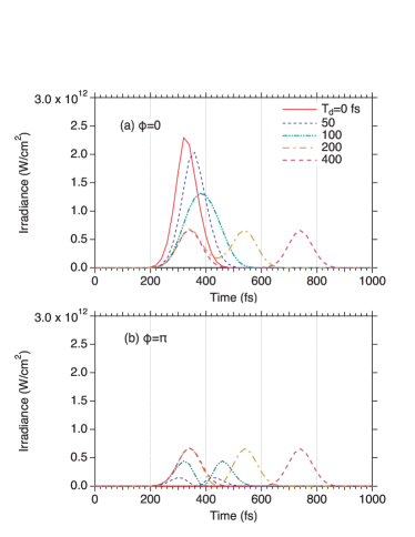
The behavior of the EM-field with constructive and destructive interference is the important point of overlapped double pulse. Figure 2 shows the time-evolution of laser field at the Si surface. The irradiance of the single pulse is W/cm2, the frequency is 1.55 eV, and the pulse duration in FWHM is 100 fs. Since our approach includes reflection at the surface, the irradiance at the surface is decreased from the incident pulse.
The constructive interference makes a 4-times more intense pulse with fs, while the destructive interference makes net zero intensity. As increases, the peak intensity of pulse approaches the intensity of a single pulse. With fs, we cannot distinguish the difference between and .
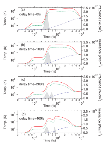
The constructive interference () may be important because it increases the efficiency of laser processing. Figure 3 shows the time-evolution of electron, hole, and lattice temperatures at the surface together with the laser irradiance. We can see an abrupt increase of electron and hole temperatures with fs. Above fs, there is a knee structure after the first pulse. In particular, with =fs, we can see a kink at the second pulse in the . This ”kink” structure in may occur with longer than the typical time scale of electron-phonon energy transfer ( fs).
In some cases, the is random. The -dependence of the -dependence at 10 ps and absorbed energy are shown in Fig. 4. The -dependence is significant in fs. The thick-solid line indicates the average. On average, the interference effect increases the to about 1.53 times and absorbed energy to about 2.5 times with respect to distinct two-pulse case ( fs).
The -dependence for fs shows slow increase as . This relatively weak -dependence may due to the -dependence of the excitation rate. The most intense -dependence in our approach is the phonon-assisted one-photon absorption in Green2008 . The increase in induces the increase of and energy absorption at the second pulse.
The two horizontal lines indicates the results with different laser parameters which gives same fluence as the case of two distinct pulses. The double-pulse excitation is more efficient than a longer pulse (200 fs), while it is less efficient than an intense pulse ( W/cm2). Since our calculation includes the two photon absorption, higher peak intensity induces more efficient photo-absorption. In the case of same peak intensity, the excitation by double pulse is efficient due to the -dependence in .
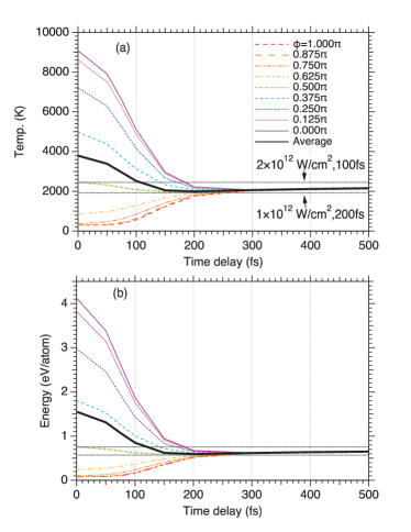
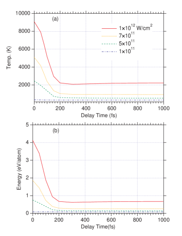
Figure 5 shows the incident intensity dependence of (a) at 10 ps and (b) absorbed energy. The intensity-dependence is significant as decreases. At intensity of W/cm2, the excitation is negligible with all , while the exceeds melting temperature (1687 K) with W/cm2, and the energy exceeds the bonding energy (2.3 eV/atom) between and W/cm2 overlapped double-pulse.
4 Summary
In this work we apply the 3TM Prachi-2022 for silicon to the double-pulse excitation process. We found that the constructive and destructive interference between the two overlapped pulses affect the excitation efficiency significantly. On the average, the overlapped double-pulse increases the efficiency about two times compared to the distinct double-pulse case. Our results indicates that we can enhance and control the excitation of silicon by the overlapped double pulse. Also, our result indicates that the excitation efficiency with two pulses increases depending on the time-delay due to the decrease of the band gap by the lattice temperature.
Aknowledgements
This research is supported by MEXT Quantum Leap Flagship Program (MEXT Q-LEAP) under Grant No. JPMXS0118067246. This research is also partially supported by JST-CREST under Grant No. JP-MJCR16N5. The numerical calculations are carried out using the computer facilities of the SGI8600 at Japan Atomic Energy Agency (JAEA).
References
- \bibcommenthead
- (1) Gattass, R.R., Mazur, E.: Femtosecond laser micromachining in transparent materials. Nat. Photonics 2(4), 219–225 (2008). https://doi.org/10.1038/nphoton.2008.47
- (2) Stoian, R., Colombier, J.-P.: Advances in ultrafast laser structuring of materials at the nanoscale. Nanophotonics 9(16), 4665–4688 (2020). https://doi.org/10.1515/nanoph-2020-0310
- (3) Sugioka, K., Cheng, Y.: Ultrafast lasers—reliable tools for advanced materials processing. Light Sci. Appl 3(4), 149–149 (2014). https://doi.org/10.1038/lsa.2014.30
- (4) Kumada, T., Akagi, H., Itakura, R., Otobe, A. Tomohitoand Yokoyama: Femtosecond laser ablation dynamics of fused silica extracted from oscillation of time-resolved reflectivity. Journal of Applied Physics 115(10), 103504 (2014) https://doi.org/10.1063/1.4867438. https://doi.org/10.1063/1.4867438
- (5) Kumada, T., Otobe, T., Nishikino, M., Hasegawa, N., Hayashi, T.: Dynamics of spallation during femtosecond laser ablation studied by time-resolved reflectivity with double pump pulses. Applied Physics Letters 108(1), 011102 (2016) https://doi.org/10.1063/1.4939231. https://doi.org/10.1063/1.4939231
- (6) Dinh, T.-H., Medvedev, N., Ishino, M., Kitamura, T., Hasegawa, N., Otobe, T., Higashiguchi, T., Sakaue, K., Washio, M., Hatano, T., Kon, A., Kubota, Y., Inubushi, Y., Owada, S., Shibuya, T., Ziaja, B., Nishikino, M.: Controlled strong excitation of silicon as a step towards processing materials at sub-nanometer precision. Communications Physics 2(1), 150 (2019). https://doi.org/10.1038/s42005-019-0253-2
- (7) Nakamura, A., Mizuta, T., Shimotsuma, Y., Sakakura, M., Otobe, T., Shimizu, M., Miura, K.: Picosecond burst pulse machining with temporal energy modulation [invited]. Chin. Opt. Lett. 18(12), 123801 (2020)
- (8) Otobe, T., Hayashi, T., Nishikino, M.: Effect of plasma formation on the double pulse laser excitation of cubic silicon carbide. Applied Physics Letters 111(17), 171107 (2017) https://doi.org/10.1063/1.4997363. https://doi.org/10.1063/1.4997363
- (9) Zhang, K.H., Li, X., Rong, W.L., Ran, P., Li, B., Feng, P., Yang, Q.Q.: Control of surface ablation on fused silica with ultrafast laser double-pulse based on seed electrons dynamics control. In: Li, L., Hong, M., Jiang, L. (eds.) AOPC 2015: Micro/Nano Optical Manufacturing Technologies; and Laser Processing and Rapid Prototyping Techniques, vol. 9673, pp. 206–213. SPIE, ??? (2015). https://doi.org/10.1117/12.2202346. International Society for Optics and Photonics. https://doi.org/10.1117/12.2202346
- (10) Zhang, J., Wang, S., Wang, M., Chu, Z.: Femtosecond laser double pulses nanofabrication on silicon. IOP Conference Series: Materials Science and Engineering 565(1), 012018 (2019). https://doi.org/10.1088/1757-899x/565/1/012018
- (11) Wang, M., Guo, Q., Wang, S., Zhu, W., Tian, F., Wei, Y., Ji, P., Li, X., Yang, J.: Interference femtosecond laser stamping of micro-grating structures and time-resolved observation of its dynamics. Opt. Express 28(12), 18376–18386 (2020). https://doi.org/10.1364/OE.390012
- (12) Drosd, R., Minkin, L., Shapovalov, A.S.: Interference and the law of energy conservation. The Physics Teacher 52(7), 428–430 (2014) https://doi.org/10.1119/1.4895362. https://doi.org/10.1119/1.4895362
- (13) Anisimov, S., Kapeliovich, B., Perelman, T., et al.: Electron emission from metal surfaces exposed to ultrashort laser pulses. Zh. Eksp. Teor. Fiz 66(2), 375–377 (1974)
- (14) Chen, J.K., Tzou, D.Y., Beraun, J.E.: Numerical investigation of ultrashort laser damage in semiconductors. Int. J. Heat Mass Transf. 48(3), 501–509 (2005). https://doi.org/10.1016/j.ijheatmasstransfer.2004.09.015
- (15) Silaeva, E.P., Vella, A., Sevelin-Radiguet, N., Martel, G., Deconihout, B., Itina, T.E.: Ultrafast laser-triggered field ion emission from semiconductor tips. New J. Phys. 14(11), 113026 (2012). https://doi.org/10.1088/1367-2630/14/11/113026
- (16) Venkat, P., Otobe, T.: Three-temperature modeling of laser-induced damage process in silicon. arXiv:2202.01964 (2022) https://arxiv.org/abs/2202.01964
- (17) Green, M.A.: Self-consistent optical parameters of intrinsic silicon at 300k including temperature coefficients. Sol. Energy Mater. Sol. Cells 92(11), 1305–1310 (2008). https://doi.org/10.1016/j.solmat.2008.06.009
- (18) Murayama, M., Nakayama, T.: Ab initio calculations of two-photon absorption spectra in semiconductors. Phys. Rev. B 52, 4986–4997 (1995). https://doi.org/10.1103/PhysRevB.52.4986
- (19) Garcia, H., Kalyanaraman, R.: Phonon-assisted two-photon absorption in the presence of a dc-field: the nonlinear franz–keldysh effect in indirect gap semiconductors. Journal of Physics B: Atomic, Molecular and Optical Physics 39(12), 2737–2746 (2006). https://doi.org/10.1088/0953-4075/39/12/009
- (20) Furey, B.J., Barba-Barba, R.M., Carriles, R., Bernal, A., Mendoza, B.S., Downer, M.C.: I{(3)} spectra of 110-cut gaas, gap, and si near the two-photon absorption band edge. Journal of Applied Physics 129(18), 183109 (2021) https://doi.org/10.1063/5.0047478. https://doi.org/10.1063/5.0047478
- (21) Fukushima, T.: Precise and fast computation of generalized fermi–dirac integral by parameter polynomial approximation. Appl. Math. Comput. 270, 802–807 (2015). https://doi.org/10.1016/j.amc.2015.08.094
- (22) Cloutman, L.D.: Numerical Evaluation of the Fermi-Dirac Integrals. Astrophys. J., Suppl. Ser. 71, 677 (1989). https://doi.org/10.1086/191393
- (23) Sokolowski-Tinten, K., von der Linde, D.: Generation of dense electron-hole plasmas in silicon. Phys. Rev. B 61, 2643–2650 (2000). https://doi.org/10.1103/PhysRevB.61.2643
- (24) Rämer, A., Osmani, O., Rethfeld, B.: Laser damage in silicon: Energy absorption, relaxation, and transport. J. Appl. Phys. 116(5), 053508 (2014). https://doi.org/10.1063/1.4891633
- (25) Sato, S.A., Shinohara, Y., Otobe, T., Yabana, K.: Dielectric response of laser-excited silicon at finite electron temperature. Phys. Rev. B 90, 174303 (2014). https://doi.org/10.1103/PhysRevB.90.174303
- (26) Terashige, T., Yada, H., Matsui, Y., Miyamoto, T., Kida, N., Okamoto, H.: Temperature and carrier-density dependence of electron-hole scattering in silicon investigated by optical-pump terahertz-probe spectroscopy. Phys. Rev. B 91, 241201 (2015). https://doi.org/10.1103/PhysRevB.91.241201
- (27) Mur, G.: Absorbing boundary conditions for the finite-difference approximation of the time-domain electromagnetic-field equations. IEEE Trans. Electromagn. Compat. EMC-23(4), 377–382 (1981). https://doi.org/10.1109/TEMC.1981.303970
- (28) van Driel, H.M.: Kinetics of high-density plasmas generated in si by 1.06- and 0.53-m picosecond laser pulses. Phys. Rev. B 35, 8166–8176 (1987). https://doi.org/10.1103/PhysRevB.35.8166
- (29) Yoffa, E.J.: Screening of hot-carrier relaxation in highly photoexcited semiconductors. Phys. Rev. B 23, 1909–1919 (1981). https://doi.org/10.1103/PhysRevB.23.1909
- (30) Sjodin, T., Petek, H., Dai, H.-L.: Ultrafast carrier dynamics in silicon: A two-color transient reflection grating study on a surface. Phys. Rev. Lett. 81, 5664–5667 (1998). https://doi.org/10.1103/PhysRevLett.81.5664
- (31) Harb, M., Ernstorfer, R., Dartigalongue, T., Hebeisen, C.T., Jordan, R.E., Miller, R.J.D.: Carrier relaxation and lattice heating dynamics in silicon revealed by femtosecond electron diffraction. The Journal of Physical Chemistry B 110(50), 25308–25313 (2006) https://doi.org/10.1021/jp064649n. https://doi.org/10.1021/jp064649n. PMID: 17165976
- (32) Ichibayashi, T., Tanimura, K.: Ultrafast carrier relaxation in si studied by time-resolved two-photon photoemission spectroscopy: Intravalley scattering and energy relaxation of hot electrons. Phys. Rev. Lett. 102, 087403 (2009). https://doi.org/10.1103/PhysRevLett.102.087403
- (33) Barber, H.D.: Effective mass and intrinsic concentration in silicon. Solid-State Electronics 10(11), 1039–1051 (1967). https://doi.org/10.1016/0038-1101(67)90122-0
- (34) Lipp, V.P., Rethfeld, B., Garcia, M.E., Ivanov, D.S.: Atomistic-continuum modeling of short laser pulse melting of si targets. Phys. Rev. B 90, 245306 (2014). https://doi.org/10.1103/PhysRevB.90.245306
- (35) Meyer, J.R., Kruer, M.R., Bartoli, F.J.: Optical heating in semiconductors: Laser damage in ge, si, insb, and gaas. J. Appl. Phys. 51(10), 5513–5522 (1980). https://doi.org/10.1063/1.327469
- (36) Dziewior, J., Schmid, W.: Auger coefficients for highly doped and highly excited silicon. Applied Physics Letters 31(5), 346–348 (1977) https://doi.org/10.1063/1.89694. https://doi.org/10.1063/1.89694