Vectorial probing of electric and magnetic transitions in variable optical environments and vice-versa
Abstract
We use europium doped single crystalline NaYF4 nanorods for probing the electric and magnetic contributions to the local density of optical states (LDOS). Reciprocically, we determine intrinsic properties of the emitters (oscillator strength, quantum yield) by comparing their measured and simulated optical responses in front of a mirror. We first experimentally determine the specifications of the nanoprobe (orientation and oscillator strength of the electric and magnetic dipoles moments) and show significant orientation sensitivity of the branching ratios associated with electric and magnetic transitions. In a second part, we measure the modification of the LDOS in front of a gold mirror in a Drexhage’s experiment. We discuss the role of the electric and magnetic LDOS on the basis of numerical simulations, taking into account the orientation of the dipolar emitters. We demonstrate that they behave like degenerated dipoles sensitive to polarized partial LDOS.
Keywords: Magnetic dipole, LDOS, nanophotonics, optical near-field probe
1 Introduction
The electromagnetic local density of states (LDOS) is a key parameter governing light-matter interaction processes such as radiative heat transfer [1, 2] or spontaneous emission [3, 4, 5] so that it is of importance for controlling heat dissipation in optoelectronics devices [6], or coherence emission of single photon source for quantum technologies [7]. Therefore, strong efforts have been put forward to map and control LDOS in the optical near-field [8, 9, 10, 11, 12, 13, 14] with more particular attention devoted to the role of electric and magnetic contributions in the last decade [15, 16, 17, 18, 19, 20]. Indeed, although light-matter interaction is mainly governed by electric dipole in the visible range, it is possible to enhance magnetic dipole contribution, opening a new parameter to control light at the nanoscale.These pionered works considered randomly oriented rare-earth ions as local probes of the electromagnetic environment. They mainly investigated fluorescence intensity, giving access to the so-called radiative LDOS, either electric or magnetic [15, 16, 17, 37]. The full LDOS, including radiative and non radiative channels for both electric and magnetic contributions, is proportional to fluorescence decay rate so that it can be probed by lifetime measurement. In 2018, Zia and coworkers measured the lifetime of ions in front of a gold mirror or dielectric interfaces and discussed the electric and magnetic contribution to the complete LDOS [18]. They used randomly oriented emitters doping thin films, probing the LDOS averaged over the field polarizations.
In this work, we consider individual europium doped NaYF4 (NaYF4:Eu3+) nanorods as quasi vectorial probes of the electric and magnetic LDOS. Eu3+ ions present both electric and magnetic dipole transitions in the optical range so that the lifetime of their excited states are sensitive to both electric and magnetic LDOS. We recently characterized the electric and magnetic optical transitions in single crystalline NaYF4:Eu3+ nanorods and demonstrated well defined orientation of the associated dipole moments [22, 23]. Moreover, the low phonon ( cm-1) NaYF4 host matrix ensures narrow electric and magnetic emission lines and facilitates their distinction in the spectra [17, 21, 22, 23, 24]. Finally, single crystalline host matrix induces well defined polarized electric dipole (ED) or magnetic dipole (MD) optical transitions, related to the nanocrystal c-axis orientation [25, 26]. The dipole transition presents a fixed orientation with respect to the rod axis and constitutes a degenerated dipole of interest for vectorial nanoprobing. Reversely, analyzing the modification of the fluorescence signal in complex environment enables to access the intrinsic properties of the emitters such as orientation [27], quantum yield [28] and oscillator strength [16].
In this article, we take benefit of these engineered optical nanosources to investigate electric and magnetic LDOS variations. In section 2.1, we determine the ED/MD orientation from polarized diagram emission measurement. Then, in section 2.2, we quantify oscillator strengths of the emitters by measuring the ED/MD branching ratio as a function of the distance to a gold mirror. Having fully characterized intrinsic optical properties of NaYF4:Eu3+ nanocrystal, we use it as a LDOS nanoprobe in a Drexhage-like experiment in section 3.
2 Specifications of the optical properties of NaYF4:Eu3+ nanoprobe
2.1 Electric and magnetic dipole moments orientation
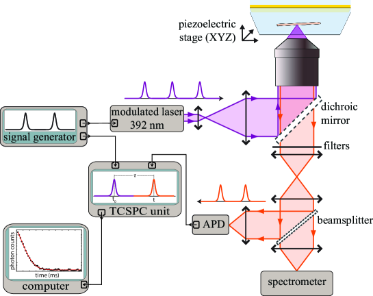
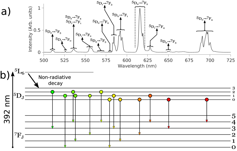
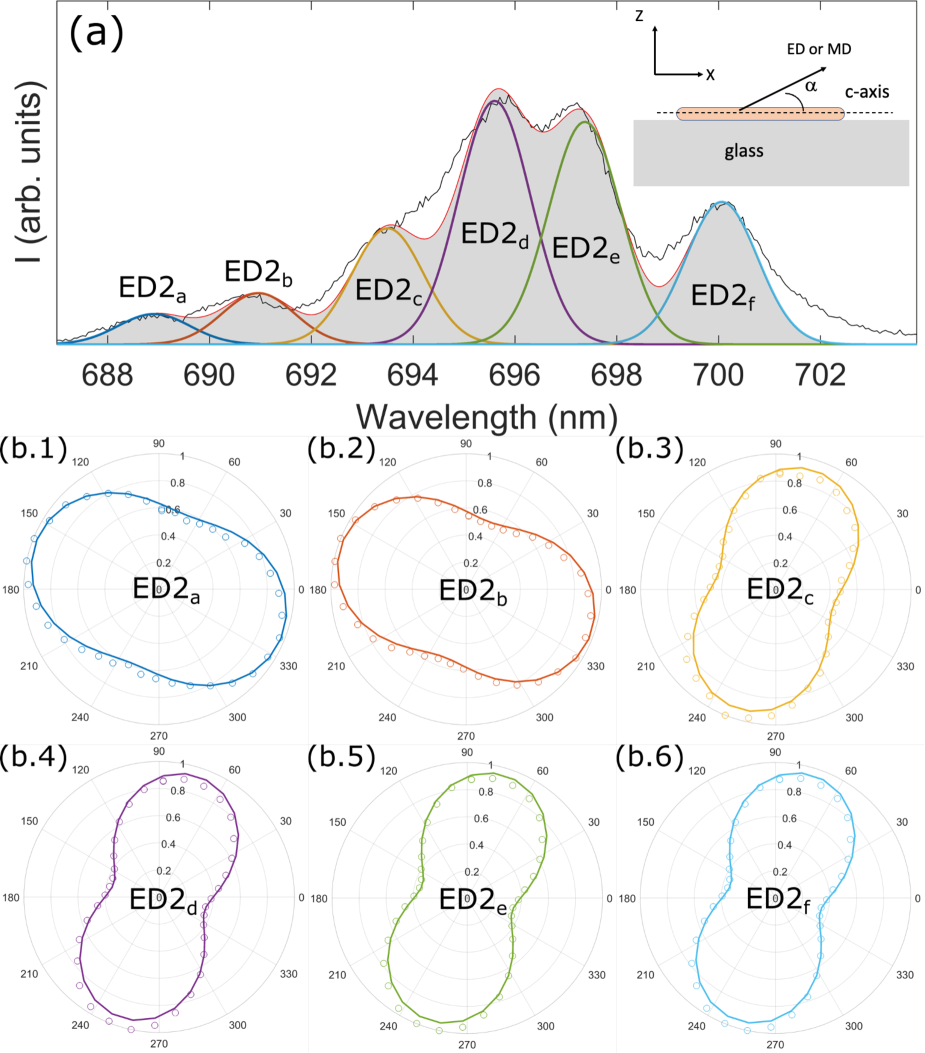
Single crystal NaYF4:Eu3+ nanorods, with average length and diameter of and 120 nm respectively, were synthesized using hydrothermal procedure described in references [29, 22]. The doped nanorods were deposited by drop-casting on a quartz coverslip bearing a grid landmark pattern. The emission spectra of single nanorod were acquired with a home-made confocal microscope, schemed in Fig. 1. The europium ions were excited by a continuous-wave (CW) laser at a wavelength of nm, focused by a low numerical aperture objective lens (NA=0.60, 40X, Nikon). The photoluminescence emission was collected through the same objective. After collection, the light was directed towards an avalanche photodiode (APD) or a spectrometer. Single nanorod spectrum is presented in Fig. 2 with the corresponding transitions lines. In the following, we focus on the three emission lines originating from the excited state 5D0: , and . Indeed, we need to characterize the dipole moments of all the optical transitions involved in the relaxation of the excited state before using it as LDOS nanoprobe. This notably requests to know the nature (electric or magnetic), the orientation and the numbers (associated to the 7FJ levels and their Stark sublevels) of the dipole moments. These properties strongly depends on the host matrix. The MD () and ED () optical transitions have been extensively investigated in ref. [22, 23]. Therefore, we summarize our method to characterize the dipolar transition moment considering the ED () transition only, for the sake of clarity. Dipole moment orientation can be deduced from polarized emission diagram. We recorded polarized emission spectra of individual rods, placing an analyser in front of the spectrometer, see Fig. 3. Scanning electron microscopy (SEM) was systematically performed after optical characterizations and only data acquired for individual rods are kept in the analysis. The crystal-field perturbation lift the degeneracy of the levels into to (2J+1) Stark sublevels [31]. In Fig. 3a) we observe six of the nine ED transitions (), noted EDa,…,f. The spectra are fitted with a sum of six Gaussian functions and the contribution of each peak (area under each Gaussian) is plotted as a function of the angle of the analyser in Fig. 3b).
Optical emission is modeled considering a single rod with its c-axis aligned with the substrate/air interface. The ED or MD moments associated to a transition line present a fixed angle with respect to the c-axis inducing that the rod emission is equivalent to the incoherent emission of three electric or magnetic orthogonal dipoles [22]
| (10) |
The dipolar angles are determined from polarized diagram emission [26, 22, 23]. For low NA objective, the detected intensity is expressed as
| (11) |
where refers to the angle of the analyzer with respect to the rod c-axis. for an electric dipole and for a magnetic dipole. So, the emitter angle with respect to the c-axis can be estimated from the fitting parameters of the measured polarized diagram. We have used exact expressions considering the NA of the objective for the sake of accuracy but the paraxial approximation can be safely used for . The fits are presented as solid lines in Fig.3b), with the parameters gathered in Table 1. ED2a and ED2b present similar angles with respect to the c-axis and close emission wavelengths ( nm, ) so that they can be treated as a unique electric dipole (noted ED2ab) in the following. Dipole moments ED2c to ED2f are all emitting around 697 nm and are oriented close to . Note that it can be sometimes difficult to unambiguously determine the angle leaving both c-axis and orientations as free parameters. However, we carefully determined the nanorod orientation and MD angle by confocal microscopy and took care that c-axis orientation is the same for ED and MD transitions, lifting the ambiguity. See ref. [22] for details.
We applied the same procedure for ED and MD transitions for several Eu3+doped nanorods. The results are summarized in Table 1. We observed three MD transitions () as expected because of the crystal field splitting of the Stark sub-levels. MD1 ( nm, ) and MD2 ( nm, ) present similar emission properties so that they can be treated as a unique magnetic dipole (MD12). MD3 ( nm, ) has to be considered separately. We also resolved two of the five ED transitions. Finally, as pointed above, we observed six of the nine ED transitions () but again with only two different angles.
| transition | |||||
|---|---|---|---|---|---|
| dipole | MD1 | MD2 | MD3 | ED1a | ED1b |
| (590 nm) | (592 nm) | (595 nm) | (615 nm) | (620 nm) | |
| 68 | 72 | 37.3 | 60.3 | 44.3 | |
| approx | MD12 (590 nm) | MD3 (595 nm) | |||
| 70∘ | 37∘ | ||||
| transition | ||||||
|---|---|---|---|---|---|---|
| dipole | ED2a | ED2b | ED2c | ED2d | ED2e | ED2f |
| (689 nm) | (691 nm) | (693 nm) | (696 nm) | (697 nm) | (700 nm) | |
| 63.4 | 62.9 | 43.3 | 40.7 | 38.7 | 38.8 | |
| approx | ED2ab (690 nm) | ED2cdef (697 nm) | ||||
| 63∘ | 40∘ | |||||
2.2 Oscillator strengths of the ED and MD transitions
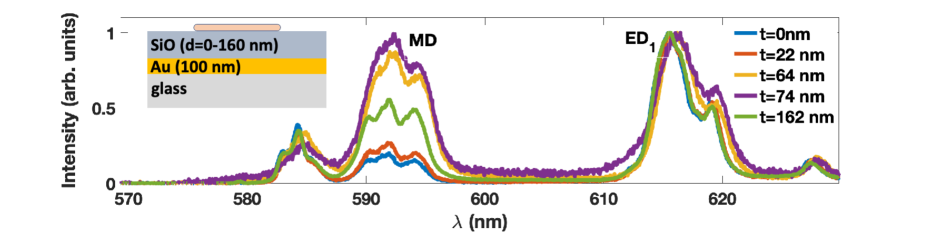
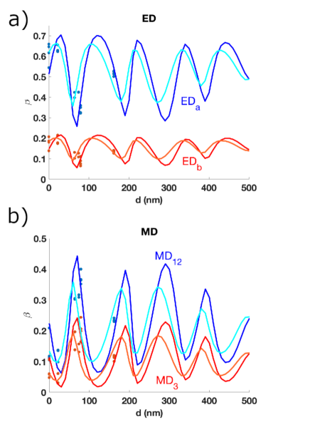
Having fully determined the orientation of the ED/MD lines, we now focus on measuring the ED/MD branching ratios for nanorods deposited on a gold mirror. This gives access to the oscillator strengths of the optical transitions, of importance to quantify the LDOS probing. A grid landmark pattern was microfabricated on glass coverslips. Over this pattern, a layer of gold was deposited by thermal evaporation to create optically thick mirrors (thickness greater than 100 nm). On the gold mirrors a film of SiO was deposited by thermal evaporation to act as a spacer. The SiO spacer thickness was measured with a stylus profilometer (Dektak 150). The samples were cleaned with oxygen plasma and afterwards, a dispersion of rods in water was drop casted on the SiO film and left to dry. Fig. 4 presents the spectra measured at different distances to the mirror. We observe a strong dependency of the MD signal with respect to the distance to the mirror, indicating a large modification of the MD/ED branching ratio.
In the previous section, we noticed that ED1 and ED2 transitions share very similar dipole orientation. Moreover, the optical signal poorly depends on the wavelength in the very near-field of the mirror were quasi-static dipole image reproduces the main features. So we simplify the discussion merging ED1 and ED2 contributions, see table 2.
| transition | MD12 (590 nm) | MD3 (595 nm) | EDa | EDb |
|---|---|---|---|---|
| 70∘ | 37∘ | 63∘ | 40∘ |
We measure the emission spectra without analyser. Spectra are again fitted by gaussian profiles and the weight of each transition (MD12, MD3, EDa, EDb) is the surface area below the corresponding gaussian (MD12 weight is the sum of MD1 and MD2 peaks areas). Finally, each transition branching ratio is estimated. For instance
| (12) |
where is the area of MD12 transition. Similar definitions occur for the other transitions.
The intensity recorded in the microscope objective is modelized as the incoherent emission of two dipoles parallel to the interface ( and ) and one dipole perpendicular to the interface (). Therefore, radiative intensity at angle for an electric dipole transition is equal to
and refer to the emission for a dipole parallel or perpendicular to the surface, respectively [34, 4]. and are the -polarized Fresnel reflexion coefficients on the air/SiO(thickness )/Au (100 nm)/glass multilayer substrate. refers to the altitude of the emitter.
The magnetic dipole intensity is straightforwardly obtained with the exchange :
| (14) | |||||
The light collected throughout an objective of numerical aperture NA=0.6 (corresponding to an acceptance angle ), for a spacer thickness is
where we integrate the radiative intensity over the NA and the rod diameter . Branching ratios can be numerically fitted from this model. For instance,
| (15) |
is the oscillator strength of the transition . Because ratio are fitted, we have only access to relative quantities . Fits are presented in Figure 5 and fitting parameters are given in table 3.
| transition | MD12 | MD3 | EDa | EDb |
|---|---|---|---|---|
| 0.34 | 0.13 | 0.77 | 0.19 |
We observe a fair agreement between the experimental data and our simulations, confirming the strong dependency of the electric and magnetic branching ratios with respect to the distance to the metallic mirror [15, 16, 17, 18]. The spatial oscillations ( nm) originate from interferences between direct dipolar emission and light reflected on the mirror (term in Eqs. 2.2,14). Moreover, we clearly observe strong differences depending on the dipole transition orientation. Namely, the branching ratio of the electric transition oscillates between 30% and 70 % for EDa () and between 5% and 25 % for EDb (). Magnetic branching ratios vary in the range 5% -45% for MD12 () and 2-25 % for MD3 (), opening the door towards vectorial probing of the electromagnetic properties. Different branching ratios for ED and MD originate from different coupling efficiency to the surface plasmon polariton depending on the dipole nature, orientation and altitude. It is worth noticing that the orientation of the dipolar emitters is defined by the angle with respect to the c-axis. Engineering the matrix host shape and anisotropy would lead to different ED or MD polarizations for vectorial probing.
3 Nanoprobing of the electric and magnetic local density of states
3.1 Relaxation channels for electric and magnetic dipolar emissions
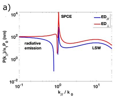
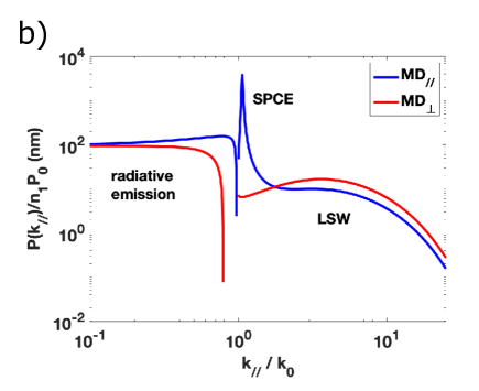
Fluorescence lifetime of an emitter depends on the distance to the mirror, as demonstrated by Drexhage [35, 3]. ED and MD emissions present different behaviours as a function of the distance to the mirror [34, 36, 37]. We represent in Fig. 6 the different relaxation channels deduced from Sommerfeld expansion of the dipolar emission as a function of the in-plane wavector [4]
| (16) |
The power spectrum is presented in Fig. 6 for ED and MD emitters. Radiative emission corresponds to the range . The Lorentzian peak at originates from surface plasmon coupled emission (SPCE) and contribution at high are associated to lossy surfaces waves (LSW) [38]. We notably observe that SPCE occurs for all the cases except for a MD perpendicular to the surface. The relaxation channel for perpendicular MD is governed by the non radiative losses (LSW). Polarized ED/MD transitions of NaYF4:Eu3+ differently couple to surface plasmon polaritons (SPP) and would be of strong interest for SPP routing [37].
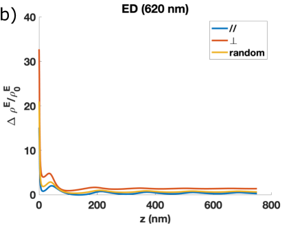
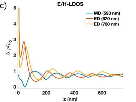
Electric and magnetic LDOS correspond to the total ED or MD emission in the complex environment and are obtained by integrating the Sommerfeld expansion of Fig. 6. Normalized LDOS are expressed as a function of electric and magnetic Green’s tensor, respectively: . refers to the electric Green’s tensor above the mirror and its expression is given in ref. [4]. refers to the magnetic Green’s tensor above the mirror and is obtained from with the exchange of the Fresnel coefficients . Note that we can safely neglect quantum effects (nonlocality, electronic spill-out, and Landau damping) on the metal optical response since their effects are not significative above few nanometers [39, 40]. Normalized electric and magnetic LDOS, averaged over the rod height, are presented in Fig. 7. The variation of the magnetic LDOS is of the order of the free space LDOS whereas the electric LDOS is enhanced up to a factor of 30, as expected from stronger ED contribution to light-matter interaction in non magnetic materials.
The decay rate of the excited states is governed by ED (5D 7F2 and 5DF4) and MD (5DF1) transitions. It is worth noticing that the emitter is a linear combination of incoherent electric and magnetic dipoles so that their decay rate contributions can be independently summed [41].
is the decay rate in free-space (including intrinsic non radiative rate). As explained above, we simplify the modelization merging the 5D 7F2 and 5DF4 contributions to a global electric contribution since they present similar ED dipole orientation. Therefore, decay rates modification induced by the optical environnement simplifies to
| (18) | |||
where is the local field correction inside the rod of optical index [17]. refers to the modification of the decay rate in front of the mirror and is expressed as a function of the transition quantum yields and partial LDOS. We also present in Fig. 7c) the variation of the electric and magnetic LDOS at the emission wavelength of 5D 7F1, 5D 7F2 and 5DF4 optical transitions. We observe that electric LDOS variations are similar in the very near-field of the mirror at 620 and 700 nm. This justifies to merge all ED presenting similar orientations.
3.2 Drexhage’s experiment
In the following, we measure the lifetime of Europium doped nanorods as probe of the electromagnetic LDOS in a Drexhage’s experiment. The confocal microscope was adapted to measure the lifetime of the photoluminescence of the Eu3+-doped nanorods, as shown in Fig. 1. The europium ions were excited by a laser emitting pulses at a wavelength of nm, modulated at 10 Hz. The photoluminescence emission was collected through the same objective and directed towards an avalanche photodiode (APD). Because of parasitic luminescence of impurities in SiO films, we first checked that we measured Eu3+ emission recording a spectrum in CW regime before modulating the laser for decay time acquisition. The emitted signal was filtered (band pass filter range between 586.8 nm and 598.6 nm - Semrock FF01-600/14, Semrock FF02-586/15) to acquire signal emitted from the the excited state only (avoiding notably the transitions at 580 nm).
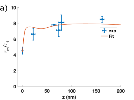
Quantum yield is proportionnal to the oscillator strength [42] so that we can rewrite the above expression (Eq. 18) with where is a proportionality factor (that depends on the materials). The only unknown parameters are the free space decay rate and the factor . Fig. 8 shows the fluorescence lifetime measured as a function of the distance to the mirror and the corresponding fitting curve. The MD and ED contributions to the decay rate (inverse of lifetime) are also presented in fig. 8b). We clearly observe that the main contribution to the decay rate originates from the ED transitions at short distances, where the variations are large. It is worth mentioning that the large LDOS observed in the very near-field of the gold mirror is associated to SPCE and LSW, that are not accessible from radiative LDOS, estimated by recording the fluorescence intensity. In addition, at short distances, the variations due to (ED1) and (ED2) transitions are similar as shown in Fig. 7c, and considering a unique ED transition may satisfactorily reproduces the evolution of the decay rate in the near-field of the mirror [43]. From the fitting parameters, one can also deduce the intrinsic non radiative rate as well as the free space radiative decay rates associated to each transition, see table 4. We found a quantum yield of 20%.
| QY | |||
|---|---|---|---|
| 103 s-1 | 7 s-1 | 14 s-1 | 20% |
4 Conclusion
We investigated in detail optical emission of NaYF4:Eu3+ nanorods in complex environments. In a first step, measuring emitted light intensity permits to determine the intrinsic optical properties of europium ions emitters in single crystalline NaYF4 nanorod host matrix; namely the dipole moment nature, orientation and relative oscillator strengths of the optical transitions. Crystal field splitting of the 7FJ level leads to Stark sublevels spectrally separated. We fully resolved the three Stark sublevels for the MD transitions () and some of them for the two ED transitions: two of the five Stark sublevels for and five of the nine Starks sublevels for . Europium doped nanorods present well defined ED/MD transitions of strong interest as vectorial nanoprobes to investigate the modification of electric and magnetic LDOS in complex environnements. Since the dipolar emitters present fixed orientation with respect to the rod long axis, they can be used as vectorial nanoprobes of the electromagnetic LDOS, as demonstrated in the second part of this work. We determined that LDOS in front of a gold mirror is mainly of electric nature. We also estimated the radiative and non radiative decay rates for both ED and MD transitions and a global quantum yield of 20%. This demonstrates rare-earth doped single crystaline NaYF4 as versatile nanoprobes of their electromagnetic environment and reciprocically that their electromagnetic environment can be used to probe their optical intrinsic properties. Further engineering of these nanoprobes would be helpfull to control the ED/MD polarization and mapping specific partial LDOS. Such nanoprobes constitute a powerful tool to characterize thermal emission and electromagnetic properties in optoelectronics devices. Deep understanding of the electric and magnetic contribution would notably help in understanding and controlling near-field radiative transfer towards low power components.
References
References
- [1] K. Joulain, J.P. Mulet, F. Marquier, R. Carminati, and J.J. Greffet. Surface electromagnetic waves thermally excited : radiative heat transfer, coherence properties and casimir forces revisited in the near field. Surf. Sci. Rep., 57:59–112, 2005.
- [2] A. E. Moskalensky and M. A. Yurkin. A point electric dipole: From basic optical properties to the fluctuation-dissipation theorem. Reviews in Physics, 6:100047, 2021.
- [3] W.L. Barnes. Fluorescence near interfaces: the role of photonic mode density. Journal of Modern Optics, 45:661–699, 1998.
- [4] G. Colas des Francs, J. Barthes, A. Bouhelier, J-C. Weeber, A. Dereux, A. Cuche, and C. Girard. Plasmonic purcell factor and coupling efficiency to surface plasmons. implications for addressing and controlling optical nanosources. Journal of Optics, 18:094005, 2016.
- [5] L. Wojszvzyk, H. Monin, and J.-J Greffet. Light emission by a thermalized ensemble of emitters coupled to a resonant structure. Advanced Optical Materials, page 1801697, 2019.
- [6] J. C. Cuevas and F. J. Garcá-Vidal. Radiative heat transfer. ACS photonics, 5:3896–3915, 2018.
- [7] P. Lodahl, S. Mahmoodian, and S. Stobbe. Interfacing single photons and single quantum dots with photonic nanostructures. Review of Modern Physics, 87:347–400, 2015.
- [8] A. Dereux, E. Devaux, J. C. Weeber, J. P. Goudonnet, and C. Girard. Direct interpretation of near–field optical images. Journal of Microscopy, 202:320–331, 2001.
- [9] A. Dereux, C. Girard, C. Chicanne, G. Colas des Francs, T. David, Y. Lacroute, and J.-C. Weeber. Subwavelength mapping of surface photonic states. Nanotechnology, 14:935, 2003.
- [10] Y. de Wilde, F. Formanek, R. Carminati, B. Gralak, P.A. Lemoine, K. Joulain, J.P. Mulet, Y. Chen, and J.J. Greffet. Thermal radiation scanning tunnelling microscopy. Nature, 444:740, 2006.
- [11] Jacob P. Hoogenboom, Gabriel Sanchez-Mosteiro, G. Colas des Francs, Dominique Heinis, Guillaume Legay, Alain Dereux, and Niek F. van Hulst. The single molecule probe: nanoscale vectorial mapping of photonic mode density in a metal nanocavity. Nano Letters, 9:1189–1195, 2009.
- [12] Mario Agio. Optical antennas as nanoscale resonators. Nanoscale, 4:692–706, 2012.
- [13] M. Kasperczyk, S. Person, D. Ananias, L. D. Carlos, and L. Novotny. Excitation of magnetic dipole transitions at optical frequencies. Physical Review Letters, 114:163903, 2015.
- [14] A. Pham, M. Berthel, Q. Jiang, J. Bellessa, S. Huant, C. Genet, and A. Drezet. Chiral optical local density of states in a spiral plasmonic cavity. Physical Review A, 94:053850, 2016.
- [15] S. Karaveli and R. Zia. Spectral tuning by selective enhancement of electric and magnetic dipole emission. Physical Review Letters, 106:193004, 2011.
- [16] L. Aigouy, A. Cazé, P. Gredin, M. Mortier, and R. Carminati. Mapping and quantifying electric and magnetic dipole luminescence at the nanoscale. Physical Review Letters, 113(076101), 2014.
- [17] F. T. Rabouw, P. T. Prins, and D. J. Norris. Europium-doped NaYF4 nanocrystals as probes for the electric and magnetic local density of optical states throughout the visible spectral range. Nano Letters, 16:7254–7260, 2016.
- [18] D. Li, S. Karaveli, S. Cueff, W. Li, and R. Zia. Probing the combined electromagnetic local density of optical states with quantum emitters supporting strong electric and magnetic transitions. Physical Review Letters, 121:227403, 2018.
- [19] P. Wiecha, C. Majorel, C. Girard, A. Arbouet, B. Masenelli, O. Boisron, A. Lecestre, G. Larrieu, V. Paillard, and A. Cuche. Enhancement of electric and magnetic dipole transition of rare-earth-doped thin films tailored by high-index dielectric nanostructures. Applied Optics, 58:1682–1690, 2019.
- [20] S. Bidault, M. Mivelle, and N. Bonod. Dielectric nanoantennas to manipulate solid-state light emission. Journal of Applied Physics, 126(094104), 2019.
- [21] J. F. Suyver, J. Grimm, M. van Veen, D. Biner, K. Krämer, and H.-U. Güdel. Upconversion spectroscopy and properties of nayf4 doped with er3+, tm and/or yb3+. Journal of luminescence, 117:1–12, 2006.
- [22] R. Chacon, A. Leray, J. Kim, K. Lahlil, S. Mathew, A. Bouhelier, J.-W. Kim, T. Gacoin, and G. Colas des Francs. Measuring the magnetic dipole transition of single nanorods by spectroscopy and fourier microscopy. Physical Review Applied, 14:054010, 2020.
- [23] J. Kim, R. Chacon, Z. Wang, E. Larquet, K. Lahlil, A. Leray, G. Colas des Francs, J. Kim, and T. Gacoin. Measuring 3D orientation of nanocrystals via polarized luminescence of rare-earth dopants. Nature Communications, 12:1943, 2021.
- [24] A. Kumar, A. Asadollahbaik, J. Kim, K. Lahlil, S. Thiele, K. Weber, J. Drozella, F. Sterl, N.S. Chormaic, A.M. Herkommer, J. Kim, T. Gacoin, H. Giessen, and J. Fick. Optical trapping and orientation-resolved spectroscopy of europium-doped nanorods Journal of Physics Photonics, 2:025007, 2020.
- [25] E. V. Sayre and S. Freed. Spectra and quantum states of the europic ion in crystals. II.Fluorescence and absorption spectra of single crystals of europic ethylsulfate nonahydrate. The Journal of Chemical Physics, 24:1213–1219, 1956.
- [26] J. Kim, S. Michelin, M. Hilbers, L. Martinelli, E. Chaudan, G. Amselem, E. Fradet, J.-P. Boilot, A. M. Brouwer, C.N. Baroud, J. Peretti, and T. Gacoin. Monitoring the orientation of rare-earth-doped nanorods for flow shear tomography. Nature Nanotechnology, 12:914–919, 2017.
- [27] B. Sick, B. Hecht, U. P. Wild, and L. Novotny. Probing confined fields with single molecules and vice versa. Journal of Microscopy, 202:365–373, 2001.
- [28] B. C. Buchler, T. Kalkbrenner, C. Hettich, and V. Sandoghdar. Measuring the quantum efficiency of the optical emission of single radiating dipoles using a scanning mirror. Physical Review Letters, 95:63004, 2005.
- [29] F. Wang, Y. Han, C. S. Lim, Y. Lu, J. Wang, J. Xu, H. Chen, C. Zhang, M. Hong, and X. Liu. Simultaneous phaseand size control of upconversion nanocrystals through lanthanide doping. Nature, 463:1061–1065, 2010.
- [30] K. Binnemans:96. Interpretation of Europium (III) spectra. Coordination Chemistry Reviews, 295:1–45, 1996.
- [31] D. Tu, Y. Liu, H. Zhu, R. Li, L. Liu, and X. Chen. Breakdown of crystallographic site symmetry in lanthanide-doped NaYF4 crystals. Angewandte Communications, 52:1128–1133, 2013.
- [32] G. Hass and C. D. Salzberg. Optical properties of silicon monoxide in the wavelength region from 0.24 to 14.0 microns. J. Opt. Soc. Am., 44(181-183), 1954.
- [33] P.B. Johnson and R.W. Christy. Optical constants of the noble metals. Physical Review B, 6:4370–4379, 1972.
- [34] W. Lukosz. Light emission by magnetic and electric dipoles close to a plane dielectric interface. iii radiation patterns of dipoles with arbitrary orientation. J. Opt. Soc. Am., 69:1495–1503, 1979.
- [35] K. H. Drexhage. Interaction of light with monomolecular dye layers. In E. Wolf, editor, Progress in Optics, volume 12, pages 161–232. North Holland, Amsterdam, 1974.
- [36] N. Noginova, R. Hussain, M. A. Noginov, J. Vella, and A. Urbas. Modification of electric and magnetic dipole emission in anisotropic plasmonic systems. Optics Express, 21:23087–23096, 2013.
- [37] R. Brechbühler, F. T. Rabouw, P. Rohner, B. le Feber, D. Poulikakos, and D. J. Norris. Two-dimensional drexhage experiment for electric- and magnetic-dipole sources on plasmonic interfaces. Physical Review Letters, 121:113601, 2018.
- [38] G. W. Ford and W. H. Weber. Electromagnetic interactions of molecules with metal surfaces. Physics Reports, 113:195–287, 1984.
- [39] S. Corni and J. Tomasi Lifetimes of electronic excited states of a molecule close to a metal surface J. Chem. Phys. ,118, 6481 2003.
- [40] P. Gonçalves and T. Christensen and N. Rivera and A.-P. Jauho and N. Asger Mortensen and M. Soljacic. Plasmon–emitter interactions at the nanoscale. Nature Communications, 11: 366, 2020.
- [41] X. Zambrana-Puyalto and N. Bonod. Purcell factor of spherical mie resonators. Physical Review B, 91:195422, 2015.
- [42] G. Hovhannesyan, V. Boudon, and M. Lepers. Transition intensities of trivalent lanthanide ions in solids: Extending the Judd-Ofelt theory. Journal of Luminescence, 241:118456, 2021.
- [43] R.E. Kunz and W. Lukosz. Changes in fluorescence lifetimes induced by variable optical environments. Physical Review B, 21:4814–4828, 1980.