Resonant plasmonic terahertz detection in gated graphene field-effect structures enabled by the Zener-Klein tunneling nonlinearity
Abstract
We show that resonant plasmonic detection dramatically increases the sensitivity of the terahertz detectors based on a gated graphene (GPIN) field-effect transistor (FET) structure. In the proposed device, the gated and regions serve as the hole and electron reservoirs and the THz resonant plasma cavities. The current-voltage () characteristics are strongly nonlinear due to the Zener-Klein interband tunneling in the reverse-biased i-region between the gates. The THz signal rectification by this region enables the THz detection. The resonant excitation of the hole and electron plasmonic oscillations results in a substantial increase in the terahertz detector responsivity at the signal frequency close to the plasma frequency and its harmonics. Due to the transit-time effects, the GPIN-FET response at the higher plasmonic modes could be stronger than for the fundamental mode. Our estimates predict the detector responsivity up to a few of V/W at room temperature, muchlarger than for other electronic THz detectors, such as Schottky diodes, p-n-junctions, Si CMOS and III-V and III-N HEMTs.
I Introduction
Short channel field-effect transistors (FETs) can serve as effective terahertz detectors [1]. Such detectors could operate in a resonant regime when the detection is strongly enhanced by plasmonic resonances or in the rectification regime when the plasmonic oscillations are overdamped. In either case, the detector responsivity is proportional to the nonlinearity of the current-voltage () characteristics. Different nonlinearity mechanisms enable the terahertz signal rectification in plasmonic FET detectors including the hydrodynamic nonlinearity and the barrier rectification in the Schottky junctions, junctions, or electrostatic barriers (see, for example, [2, 3, 4]). The FET detectors with the graphene layer (GL) channel can exhibit markedly enhanced performance [5, 6, 7, 8, 9, 10, 11, 12] due to the unique electron and hole transport properties of GLs [13, 14, 15, 16], in particular, high electron (hole) mobility and directed velocity at elevated temperatures. The specific features of the GL band structure enable the Zener-Klein interband tunneling [17, 18, 19, 20, 21, 22] leading to a very strong nonlinearity that can be used for the rectification and detection of the terahertz signals. In this paper, we evaluate the proposed THz detector based on a lateral graphene FET (GPIN-FET) detector structure with the gated p- and n-regions of the GL channel. This device combines the advantages of the strong nonlinearity and plasmonic resonant detection enhancement enabled by high carrier mobility in GLs and transit-time effects. Such a combination of high nonlinearity and plasmonic effects leads to a remarkably high responsivity. Our estimates predict the detector responsivity up to a few V/W, markedly exceeding that of Schottky diodes, p-n junctions, Si CMOS, and III-V and III-N HEMTs.
II Model
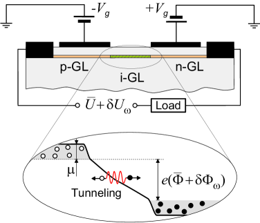
We consider the GPIN-FET detector structure based on a GL channel embedded in the dielectric [for examample hexagonal boron nitride (-BN)]. The channel is covered by two highly conducting gates. The gate voltages of different polarity, , are applied to these gates. As a result, the channel comprises the undoped regions between the gates (of the length ) and the electrically doped p and n regions beneath the gates (of the length ). The lengths of the and regions are close to the length of the gates ( is somewhat larger than the gate length due to the finite screening length or the gate fringe effect). The channel is bounded by the source and drain contacts, between which the bias voltage is applied. Figure 1 shows the GPIN-FET structure with the electrically disconnected gates and the potential profile in the GPIN-FET channel at the dc condition (inset) when the bias voltage is applied between the side (source/drain) contacts.
In the present paper, we consider the GPIN-FET structures, where the Coulomb drag effect in the gated regions [23, 24, 25, 26, 27, 28] is weak. This corresponds to GPIN-FET structures, in which more liberal and rather practical conditions are fulfilled: stronger scattering on impurities, defects, and acoustic phonons (with the collision frequencies ps-1), and relatively long gated regions (m). The region is assumed to be fairly short [(m), so that the transport of the holes and electrons generated in this region due to the Zener-Klein tunneling is ballistic [29, 30, 31, 32, 33]. Considering that the i region is depleted under the operational conditions, the conditions of the ballistic transport in this region with the above length can be realized even at room temperature [34] and, naturally, at lowered temperatures [35]. The holes and electrons generated due to tunneling are directed primarily along the electric field in the region, i.e., in the -direction (the in-plane direction along the GL channel) from the and region, and propagate ballistically with the velocities, .
Apart from the dc bias voltage , an ac signal voltage is applied, where and are the amplitude and frequency of the incoming terahertz signal. Thus, both the dc and ac voltage drops across the GPIN-FET structure are equal to and , where and are the dc and ac components of the load voltage. These components depend on the load impedance . The latter can be presented as , where and are the load resistance and capacitance, respectively. We assume that is sufficiently large, so that the ac voltage drop across it is negligibly small, therefore, and . The real part of the load impedance, i.e., its resistance, determines the dc output signal.
III Linear response
When both the dc voltage and the periodic signal voltage drop across the GPIN-FET intrinsic part [], the carrier current density in the region (and in other sections of the channel) is equal to . Here is the dc component. The component comprises the linear ac component proportional to and the ac rectified component . The latter is due to the nonlinear characteristics of the region at the conditions of the Zener-Klein tunneling.
The voltage across the devices is distributed between the region and the gated regions.
Dynamic conductance of the region
Considering the bladelike configuration of the conducting areas surrounding the region, the pertinent spatial electric-field distribution in this region [36, 37, 38, 39], and using the general formulas for the Zener-Klein tunneling probability in graphene [17, 18, 19], one can arrive at the following expression for the dc current density per unit width in the direction along the gate edges [22]:
| (1) |
where is a numerical parameter. At moderate when the carrier space charge in the regions is weak,
where is the Gamma function. Equation (1) corresponds to the i-region linear dynamic ac conductance (see Appendix A)
| (2) |
Here, is the region DC differential conductance, is the region recharging time, and is the geometrical capacitance per unit width of the device determined mainly by the dielectric constant of the isolating material surrounding the GL, and geometrical parameters (see, for example, [36, 37, 38, 39]). If the GL is deeply embedded into the isolating material . In the case of free GL top surface between the gates, . A thin passivation layer can also affect .
According to Eq. (1),
| (3) |
where . The quantity
| (4) |
reflects the signal frequency dependence of the region dynamic conductivity determined by the ac current induced by the carriers propagating between the and regions (and the pertinent gates), particularly, by the finiteness of their transit time , where is the Bessel function of the first kind.
Using Eqs. (2) and (4), we obtain the following expressions for the real and imaginary parts of :
| (5) |
| (6) |
The quantity Re can be both positive and negative. However, at , Re . In the range , where , the first term on the right-hand side of Eq. (6) is positive. The latter implies that this term corresponds to the kinetic inductance of the holes and electrons in the region. In certain ranges of elevated frequencies, the product can be positive, although both factors are negative.
For m and mV, Eqs. (1) and (4) yield A/cm and in the range from 520 - to 733 S/m (from 4.67-6.59 ps-1). In the case of a sufficiently short region, the ballistic transport takes place even at higher voltages despite the spontaneous emission of optical phonons, and the current density through this region and, hence, the differential conductance can substantially exceed the above estimates.
Considering Eq. (2), we arrive at the following equation for the linear ac current density in the region expressed via the ac potential drop across this region:
| (7) |
Plasmonic response of the gated regions
To express via , we find the spatial distributions of the ac potential in the gated region accounting for its nonuniformity associated with the plasmonic effects.
For the densities of the ac current in and regions ( and ), we have
| (8) |
where and are the and regions (gated) ac and dc conductances, respectively, is the frequency of hole and electron momentum relaxation on impurities, acoustic phonons, and expresses the ac potential spatial distribution along the axis directed in the GPIN-FET-channel plane (). The frequency dependence given by Eq. (8) accounts for the kinetic inductance of the gated regions.
For the gated sections of the channel [see Fig. 1(a)], we solve the linearized hydrodynamic equations for the hole and electron plasmas in the related and regions, disregarding the nonuniformity of the dc potential and carrier density distributions, and arrive at the following equation for the spatial distribution of the ac potential accounting for the plasmonic response of the gated regions (see [12] and the references therein):
| (9) |
Here the upper/lower sign is related to the region/ region, is the plasma velocity, and is the carrier Fermi energy in the gated regions of both types.
The quantity characterizes the contact-gate coupling, where [or ] and being the pertinent capacitances for the bladeike contacts and gates, where is the gate layer thickness. Normally, , hence .
Equation (9) governs the ac potential in the region () and in the region (). It accounts for both the gate and contact-gate capacitances and the kinetic inductance of the holes and electrons in the gated regions.
The boundary conditions at the edges of the gated regions are:
| (10) |
| (11) |
Sample (m) (ps) (ps) (m) (nm) (meV) (ps-1) (THz) a-1* 0.2 0.2 0.1 1.0 15 4.5 100 1.0 12 1.0 a-2 0.2 0.2 0.1 1.0 15 4.5 100 2.0 6 1.0 a-3 0.2 0.2 0.1 1.0 15 4.5 100 3.0 4 1.0 b-1* 0.2 0.2 0.1 1.0 15 4.5 100 1.0 12 1.0 b-2 0.1 0.1 0.1 1.0 15 4.5 100 1.0 8.5 1.0 b-3 0.4 0.4 0.1 1.0 15 4.5 100 1.0 16.9 1.0 c-1* 0.2 0.2 0.1 1.0 15 4.5 100 1.0 12 1.0 c-2 0.2 0.2 0.1 1.0 15 4.5 144 1.0 14.4 1.2 c-3 0.2 0.2 0.1 1.0 15 4.5 64 1.0 9.6 0.8 d-1* 0.2 0.2 0.1 1.0 15 4.5 100 1.0 12 1.0 d-2 0.2 0.2 0.2 1.0 33 10.0 100 1.0 12 1.0 d-3 0.2 0.2 0.3 1.0 50 15.0 100 1.0 12 1.0
Using the solution of Eqs. (9) - (11) [see Appendix B, Eqs. (B11) and (B12)] and considering that we obtain
| (12) |
with . Here
| (13) |
Here the following notations have been introduced: , . The quantity
Equation (14) accounts for the fact that the electron liquid in the gated portion of the channel at the carrier densities under consideration is degenerate.
Considering that in the real case , the function is weakly sensitive to the contact-gate capacitive coupling, in particular, to the parasitic capacitance (see Sec. VII), and Eq. (13) can be somewhat simplified as
| (15) |
.
IV Rectified current and plasmonic factor
The characteristic given by Eq. (1) corresponds to the nonlinear current density component, which comprises the rectified component and the ac current harmonics:
| (16) |
where
| (17) |
is the parameter characterizing the nonlinearity of the region tunneling characteristics given by Eq. (1), i.e., the curvature of these characteristic.
According to the Kirchhoff law,
| (18) |
where . Here we accounted for the fact that the region dc conductance is equal to .
Equation (16) yields the following expression for the density of the rectified current :
| (19) |
As seen from Eq. (19), the rectified current density , as will be seen in the following, and the frequency dependence of the GPIN-FET detector responsivity, are determined by the plasmonic factor . According to Eq. (16), this factor is given by:
| (20) |
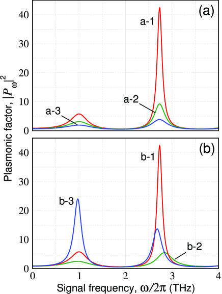
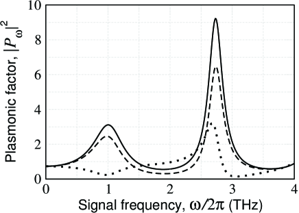
Figure 2 shows the frequency dependences of the plasmonic factor calculated for the GPIN-FETs with m, nm, meV, , ps-1(), THz, and at mV, i.e., mV and (see Table I).
As seen in Fig. 2, and, consequently, the rectified current components given by Eqs. (19), exhibit two pronounced maxima (in the frequency range under consideration, THz).
The first maximum at THz corresponds to the signal frequency close to the gated regions plasma frequency . It is obviously related to the excitation (by the incoming signal) of the fundamental mode of standing plasma wave with the wave number and the maximum amplitude at having the opposite phases. As a result, and are maximal. The collisional damping of this plasma oscillations results in lowering of the plasma resonance peaks [see the curves corresponding to different in Fig. 2(a)].
The second resonant peaks of at THz seen in Fig. 2 correspond to the excitation of the plasmonic mode with the wave number . It is instructive that the peaks associated with this mode can be higher than those related to the fundamental mode.
At elevated signal frequencies Eqs. (19) and (20) yield
| (21) |
where
For the parameters of samples (a-1) - (a-3), we obtain THz. The roll-off of and with increasing frequency is determined by the charging time , i.e., is associated with the region geometrical capacitance . Considering that , one can find that is independent of .
V GPIN-FET detector responsivity
The current responsivity (ampere-watt) of GPIN-FETs operating as the terahertz detectors is given by
| (22) |
where is the lateral size of the GPIN-FET in the direction perpendicular to the gate edges, and are the antenna aperture and gain, and are the wavelength and intensity of the incoming radiation, and is the speed of light in vacuum. Considering that , using Eq. (22), we obtain
| (23) |
For the voltage (volt-watt) responsivity , assuming that the load resistance is optimized (, i.e., if ), we arrive at the following universal formula:
| (24) |
For mV, we obtain V/W. If m, m, and mV, the optimized load resistance is equal to . Naturally, the plasmonic resonance may lead to .
A decrease in and, hence, in with the rise of the bias dc voltage is attributed to a decrease in the current-voltage characteristic nonlinearity parameter [see Eq. (17)], and to a decrease in the channel resistance with rising bias voltage . The latter requires the pertinent decrease in the optimized load resistance . However, lowering of the bias voltage is limited by the thermionic and thermogeneration processes in the region.
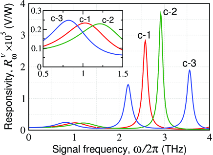
Figure 3 shows the GPIN-FET responsivity as a function of the signal frequency calculated using Eqs. (23) and (24) involving Eq. (20) for the devices (c-1) - (c-3) with the parameters presented in Table I assuming mV.
First of all, one can see that GPIN-FETs can reveal fairly high peak responsivity. Second, the responsivity peaks corresponding to the higher plasma modes can be markedly higher than the fundamental peak (see the discussion in Sec. VI). Third, the second peaks (c-1 and c-2) are positioned at the frequencies somewhat lower than THz and THz, respectively. As mentioned in Sec. IV, this is due to the effect of the region capacitance on the resonant frequency deviating it from the plasma frequency of the gated region . The same is valid for the second and third peaks c-3 in the main plot and the inset.
VI Discussion (Analysis)
Temperature dependence and heights of the resonant peaks
The obtained formulas for the GPIN-FET responsivity do not explicitly account for the temperature dependence, at least at , i.e., in the situations under consideration. This is because of the tunneling nature of the current in the GPIN-FETs. However, the plasmonic resonant factor, which determines the maximum values of is sensitive to the collision frequency . The latter is usually smaller at lower temperatures due to a decrease in the carrier momentum relaxation on acoustic phonons. Hence lowering of the temperature can result in a marked sharpening of the resonant responsivity peaks and promote a substantial increase in the resonant responsivity.
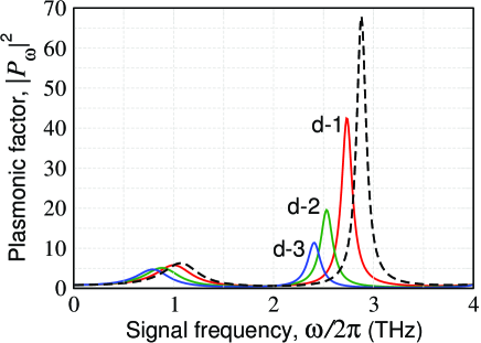
Figures 2 and 3, show some deviation of the resonant peaks position from the exact plasmonic resonances THz and THz - the peaks are shifted toward smaller frequencies. This is attributed to the collisional damping and to the contribution of the i-region geometrical capacitance. Indeed, as seen from Fig. 4, the GPIN-FETs with longer charging time , i.e., a larger region geometrical capacitance due to a larger dielectric constant of the gate layer (and the same collisional frequency ) exhibit smaller resonant frequencies. The gate layer in the samples (a-1) - (d-1) is assumed to be made of -BN (), whereas the gate layers in the samples d-2 and d-3 are made of SiC () and HfO2 (), respectively.
Table I lists the values of for the samples under consideration. The assumed value of for GPIN-FET passivated by -BN is close to its in-plane value because the in-plane direction of the electric field . The-high-frequency dielectric constant of crystalline -BN in plane is and out-of plane [44]. However, the exact effective value of depends on the thickness of the top passivating layer. GPIN-FETs could use passivating layers with very low values of , such as polyimide, porous BN/polyimide composites, or amorphous -BN with the measured dielectric permittivity of 1.16 (close to that of air) [45, 46, 47]. In Fig. 4, we also added the plot (see the dashed curve) corresponding to the parameters similar to those of the sample d-1, but with a shorter charging time (smaller dielectric constant, ). As seen, the pertinent peak is shifted weaker than others. This confirms that the region geometrical capacitance markedly affects the plasmonic resonances.
The most intriguing feature of the and frequency dependences is the larger height of the peaks corresponding to a higher plasmonic mode. Compare the plasmonic factors at the fundamental and second resonances. The plasmonic factor near the fundamental () and the second () resonances (at ), , and is equal to
| (25) |
and
| (26) |
respectively.
Considering that the product and, therefore, the denominators on the right-hand sides of Eqs. (25) and (26) are independent of , one can find that and . Such dependences of the plasmonic factor peaks on are in line with the plots in Fig. 1(a).
As follows from Eqs. (25) and (26), the ratio of the peak heights corresponding to the fundamental and second resonances, at sufficiently large values , is equal to
| (27) |
This quantity can be smaller or larger than unity, depending on . For all the samples considered above (except b-3), ; hence, the plasmonic resonances at is stronger than those at . This corresponds to the curves (a-1) -(b-2) in Fig. 2. In contrast, case b-3 is related to . In particular, for samples a-1 and b-1, we obtain , , and . This agrees well with the numerical calculation results shown in Fig. 2.
As mentioned above, the height of and resonant peaks decreases with increasing collision frequency . This is due to the strengthening of the plasma oscillation collisional damping. The hole and electron viscosity also damp the plasma oscillations, particularly, those with larger wavenumbers . This might be a reason for some lowering of the resonant peaks corresponding to higher plasma oscillations modes. The effect of the viscosity can be accounted for by replacing by where is the electron viscosity [1, 32, 48, 49]. For the fundamental, second, and third plasma modes with , and , the wavenumbers are , , and . If m, setting ps-1 and cm2/s (depending on the carrier density and the temperature [32, 48, 49]), and , these estimates show that the viscosity effect can decrease the heights of the second and fundamental peaks if the viscosity is sufficiently strong. As a result, the quantity (for example, for the samples a-1 and b-1) can vary from at to and at cm2/s and cm2/s, respectively. Lowering of the fundamental resonant peak is markedly smaller – about (2 -12) . However, the second resonance remains stronger even at relatively high viscosity.
In addition to the carrier collisions and the plasma viscosity mentioned above, the damping mechanisms include plasmon-plasmon interactions, radiative damping, scattering of plasmons on defects, dopant-induced plasmon decay, and the interaction of the hole and electron plasma with the carriers in highly conducting contacts (see, for example, [50, 51, 52, 53, 54, 55, 56, 57, 58]). The intrinsic lifetime of plasmons in GLs with the carrier densities assumed in our calculations is about 20 - 120 ps [51], i.e., much longer than the characteristic collision time . In sufficiently short GLs, the plasmon decay time due to the contacts is of the order of [54]. These estimates justify the assumption that in the GPIN-FETs under consideration the collisional and viscosity damping mechanisms dominate.
As for the third resonant peaks with and , the plasma oscillation damping due to the viscosity is strong enough to lead to the peak extinction (the right most peak in Fig. 3) at cm2/s and higher.
Effect of the contacts and gates coupling
As follows from Eq. (13), the plasmonic factor depends to some extent on the capacitive coupling between the side contacts and the gates. Figure 4 shows examples of the versus signal frequency for the GPIN-FETs with the parameters corresponding to the sample a-2 for [as in Fig. 2(a)] and for at mV. One can see that an increase in leads to resonant peaks lowering. Although one needs to keep in mind that the value corresponds to an overestimated contact-gate capacitance compared to typical values for FETs. For the comparison, we calculate also for a similar device structure, but with the short-cut side contacts and gates. In the latter case, one can use the following formula [coinciding with Eq. (20) with ]:
| (28) |
The pertinent dependence is shown in Fig. 5 as a dotted line. As seen in the latter case, the plasma resonance associated with the gated regions (at ) is suppressed, while the plasmonic resonance at is sufficiently pronounced although being relatively weak.
Thermionic and thermogeneration currents in the reverse-biased region
When becomes relatively low, the reverse thermionic current in the reverse-biased region can be comparable with the tunneling current. Considering the tunneling current [given by Eq. (1)] and the saturation current [given by Eq. (C2)], ], we find the following limitation for the minimal value of at which the tunneling dominates over the thermionic processes:
| (29) |
For m, meV, and meV, we obtain meV. This condition is satisfied in the above estimates and calculations.
The thermogeneration of the electron-hole pairs in the reverse-biased graphene junction is primarily associated with the interband absorption of optical phonons. The thermionic rate at room temperature is estimated as cm-2s-1 [59] . For m, the latter yields A/cm. For comparison, the tunneling current density in the reverse-biased junction given by Eq. (1) for the same lengths of the region at meV, is equal to A/cm, i.e., one order of magnitude larger. This implies that the dark current in the GPIN-FETs in the conditions under consideration is determined by the interband tunneling in the regions.
Joule heating
The Joule power in the GPIN-FET is equal to . For mV ( mV), A/cm. Assuming the device width m, for the Joule power we obtain W. Since the bias voltage drops primarily in the i-region and somewhat around it, the Joule power releases in the area of about . This corresponds to the thermal power density . For cm2, we obtain kW/cm2. The latter thermal power density is much lower than that, which can be supported by GFETs (up to 210 kW/cm2 [60, 61]). Hence, the Joule heating should not lead to a marked overheating of the GPIN-FET channel. Indeed, the heat flow from the GPIN-FET channel through, for example, the -BN substrate can be estimated considering the hBN thermal conductivity W/mK [62]. Assuming the thickness of the hBN layer m, we for the thermal conductivity per unit area kW/cm2K. This implies that, in such a case, the Joule heating results in an increase of the channel temperature by K. Since graphene has a high room-temperature thermal conductivity (about kW/mK) [63], the heat can also be effectively carried to the side (metallic) contacts.
Comparison of the Zener-Klein tunneling nonlinearity mechanisms with some other mechanisms
It appears natural to compare the mechanisms of the current rectification in the GPIN-FETs under consideration and in similar detectors (for example, [9]). In the latter devices, the characteristic nonlinearity in the forward-biased graphene junction is used. The pertinent nonlinearity parameter is given by Eq. (C3). Comparing the quantities [see Eq. (17)] and (for in the case of the detector using the nonlinearity) and for the GPIN-FET, we obtain
| (30) |
Setting m, meV, mV, mV, at meV ( K )we obtain . At the temperatures below room temperature, this ratio can be markedly larger. For example, at meV [ K], we obtain .
VII Conclusions
We demonstrate that the proposed GPIN-FETs detectors using the signal rectification due to the nonlinearity of the Zener-Klein tunneling characteristics can exhibit high responsivity in the terahertz range of frequencies. The responsivity can be particularly high at the signal frequencies close to the fundamental and triple carrier plasma frequency. This is due to the resonant excitation of plasma oscillation in the gate region of the GPIN-FET channel. The GPIN-FETs can demonstrate competitive resonant responsivity at room temperatures. At lower temperatures, the responsivity can markedly increase due to the reinforcement of the resonant response because of a weakening of the carrier momentum relaxation.
Acknowledgments
The Japan Society for Promotion of Science (KAKENHI Grants No. 21H04546 and No. 20K20349), Japan; RIEC Nation-Wide Collaborative Research Project No. R04/A10; the US Office of Scientific Research Contract N00001435, (project monitor Dr. Ken Goretta).
The authors declare no conflict of interest related to this article.
Appendix A
Dynamic tunneling conductance of the reverse-biased region
The injected holes and electrons propagating in the region induce the current in the surrounding highly conducting (gated) regions. The dynamical conductance, apart from the dc differential conductance of the reverse-biased region found from Eq. (1), should account for the displacement current associated with the geometrical capacitance . Therefore, the dynamical conductance of the region associated with the propagating carriers can be presented as
| (A1) |
Because of a strong nonuniformity of the electric field in the region, the tunneling generation of the electrons and holes occurs near the edges of the and regions, respectively. If the generated holes and electrons propagate across the region ballistically, their velocities are equal to . Therefore, the ac electron and hole currents are proportional to and . Hence, the ac current induced by the propagating carriers is proportional to
where, for the case of the device geometry under consideration (bladelike conducting areas), the form factor is given by [64]. This leads to
| (A2) |
where and is the Bessel function of the first kind.
If the potential drop , the optical phonon emission can delay the holes and electrons propagation in the region. For markedly exceeding 200 mV, the spatial dependence of the carrier velocity can be presented as , where ps [58] is the time of the optical phonon spontaneous emission. For the average transit time , we obtain . For m, the latter estimate yields .
Appendix B
In the gradual channel approximation, the spatiotemporal distributions of the electron and hole densities, and , in the gated regions are related to the channel potential, , and the gate potentials, and , as
| (B1) |
| (B2) |
where and are the gate layer dielectric constant and thickness. If the side source/drain contacts and the gates are coupled by a capacitive link associated with a free-space parasitic contact-gate capacitance [see Fig. 1(a)],
| (B3) |
| (B4) |
where and are the contact-gate and gate-channel capacitances, respectively.
For the dc electron and hole densities, from Eqs. (B1) and (B2) we obtain
| (B5) |
| (B6) |
with . Since normally the dc bias voltage , in Eqs. (B5) and (B6) we omit the spatially nonuniform terms with .
For the Fourier ac components, Eqs. (B1) - (B4) yield
| (B7) |
| (B8) |
Since the load resistance is shunt by a large capacitance and the drop of the ac potential across the load resistor is insignificant, .
As usual, considering the linearized hydrodynamic equations, expressing the electron and hole average velocities, and , via the ac electric field , and substituting and into the continuity equation, we obtain
| (B9) |
| (B10) |
where is the fictitious electron/hole mass in graphene. Expressing and via the carrier Fermi energy, , in the gated region, we arrive at Eq. (9) in the main text.
If the side contacts and the gates are shortened, one can again obtain Eq. (16), but with .
Solving Eq.(9) with the boundary conditions given by Eqs. (10) and (11), we obtain
| (B11) |
| (B12) |
for the region and region ), respectively. Here , , and
| (B13) |
is the plasma frequency of the gated regions.
Appendix C
The thermionic dc current density, including both the hole and electron components, in the region of the GPIN-FETs under consideration can be presented as
| (C1) |
where
| (C2) |
is the graphene junction saturation current density. In Eq. (C1), as in the main text, the junction reverse and forward bias voltages and , respectively.
Equations (C1) and (C2) yield the following value of the characteristic nonlinearity parameter:
| (C3) |
Here is the differential conductance.
References
- [1] M. I. Dyakonov and M. S. Shur, “Plasma wave electronics: novel terahertz devices using two-dimensional electron fluid,” IEEE Trans. Electron. Devices 43, 1640(1996).
- [2] V. V. Popov, N. Pala, and M. S. Shur, “Room temperature terahertz plasmonic detection by antenna arrays of field-effect transistors,” Nanosci. Nanotechnol. Lett. 4, 1015 (2012).
- [3] T. Otsuji, T. Watanabe, S. A. Boubanga Tombet, A. Satou, W. M. Knap, V. V. Popov, M. Ryzhii, and V. Ryzhii, “Emission and detection of terahertz radiation using two-dimensional electrons in III–V semiconductors and graphene,” IEEE Trans. Terahertz Sci. Technol. 3, 63 (2013).
- [4] T. Otsuji, T. Watanabe, S. A. Boubanga Tombet, A. Satou, V. Ryzhii, V. Popov, and W. Knap, “Emission and detection of terahertz radiation using two-dimensional plasmons in semiconductor nanoheterostructures for nondestructive evaluations,” Opt. Eng. 53, 031206 (2014).
- [5] L. Vicarelli, M. S. Vitiello, D. Coquillat, A. Lombardo, A. C. Ferrari, W. Knap, M. Polini, V. Pellegrini, and A. Tredicucci, “Graphene field-effect transistors as room temperature terahertz detectors,” Nat. Mat. 11, 865 (2012).
- [6] A. Zak, M. A. Andersson, M. Bauer, J. Matukas, A. Lisauskas, H. G. Roskos, and J. Stake, “Antenna-integrated 0.6 THz FET direct detectors based on CVD graphene,” Nano Lett. 14, 5834 (2014).
- [7] V. Ryzhii, M. Ryzhii, M. S. Shur, V. Mitin, A. Satou, and T. Otsuji, “Resonant plasmonic terahertz detection in graphene split-gate field-effect transistors with lateral p-n junctions,” J. Phys. D: Appl. Phys. 49, 315103 (2016).
- [8] D. Yadav, S. Boubanga-Tombet, T. Watanabe, S. Arnold, V. Ryzhii, and T. Otsuji, “Terahertz wave generation and detection in double-graphene layered van der Waals heterostructures, ”2D Mater. 3, 045009 (2016).
- [9] D. V. Fateev, K. V. Mashinsky, and V. V. Popov, “Terahertz plasmonic rectification in a spatially periodic graphene,” Appl. Phys. Lett. 110, 0611106 (2017).
- [10] I. A. Gayduchenko, G. E. Fedorov, M. V. Moskotin, D. I. Yagodkin, S. V. Seliverstov, G. N. Goltsman, A. Yu. Kuntsevich, M. G. Rybin, E. D. Obraztsova, V. G. Leiman, et al., “Manifestation of plasmonic response in the detection of sub-terahertz radiation by graphene based devices,” Nanotechnology 29, 245204 (2018).
- [11] D. A. Bandurin, D. Svintsov, I. Gayduchenko, S. G. Xu, A. Principi, M. Moskotin, I. Tretyakov, D. Yagodkin, S. Zhukov, T. Taniguchi, K. Watanabe, I. V. Grigorieva, M. Polini, G. N. Goltsman, A. K. Geim, and G. Fedorov, “Resonant terahertz detection using graphene plasmons,” Nat. Comm. 9, 5392 (2018).
- [12] V. Ryzhii, T. Otsuji, and M. S. Shur, “Graphene based plasma-wave devices for terahertz applications,” Appl. Phys. Lett. 116, 140501 (2019).
- [13] P. R. Wallace, “Band theory of graphite,”Phys. Rev. 71, 622 (1947).
- [14] A. H. Castro Neto, F. Guinea, N. M. R. Peres, K. S. Novoselov, and A. K. Geim, “The electronic properties of graphene,” Rev. Mod. Phys. 81, 109 (2009).
- [15] T. Low and Ph. Avouris, Graphene plasmonics for terahertz to mid-infrared applications,” ACS Nano, 8, 1086 (2014).
- [16] Y. Li, K. Tantiwanichapan, A. K. Swan, and R. Paiella, “Graphene plasmonic devices for terahertz optoelectronics,”Nanophotonics 9 1901 (2020).
- [17] V. V. Cheianov and V. I. Fal’ko, “Selective transmission of Dirac electrons and ballistic magnetoresistance of junctions in graphene,” Phys. Rev 74, 041103 (2006).
- [18] A. Ossipov, M. Titov, and C. W. J. Beenakker, “Reentrance effect in a graphene junction coupled to a superconductor,” Phys. Rev. B 75, 241401(R) (2007).
- [19] D. Jena, “Tunneling transistors based on graphene and 2-D crystals,” Proc. IEEE 101, 1585 (2013).
- [20] N. Vandecasteele, A. Barreiro, M. Lazzeri, A. Bachtold, and F. Mauri, “Current-voltage characteristics of graphene devices: Interplay between Zener-Klein tunneling and defects,” Phys. Rev. B 82, 045416 (2010).
- [21] V. Ryzhii, M. Ryzhii, V. Mitin, and M. S. Shur, “Graphene tunneling transit-time terahertz oscillator based on electrically induced p-i-n junction,” Appl. Phys. Exp. 2, 034503 (2009).
- [22] V. L. Semenenko, V. G. Leiman, A. V. Arsenin, V. Mitin, M. Ryzhii, T. Otsuji, and V. Ryzhii, “Effect of self-consistent electric field on characteristics of graphene p-i-n tunneling transit-time diodes, ” J. Appl. Phys. 113, 024503 (2013).
- [23] J. C. Song, D. A. Abanin, and L. S. Levitov, “Coulomb drag mechanisms in graphene,” Nano Lett. 13, 3631 (2013).
- [24] M. Schütt, P. M. Ostrovsky, M. Titov, I. V. Gornyi, B. N. Narozhny, and A. D. Mirlin, “Coulomb drag in graphene near the Dirac point,” Phys. Rev. Lett. 110, 026601 (2013).
- [25] R. V. Gorbachev, A. K. Geim, M. I. Katsnelson, K. S. Novoselov, T. Tudorovskiy, I. V. Grigorieva, A. H. MacDonald, S. V. Morozov, K. Watanabe, T. Taniguchi, and L. A. Ponomarenko, “Strong Coulomb drag and broken symmetry in double-layer graphene,” Nat. Phys. 8, 896 (2012).
- [26] V. Ryzhii, M. Ryzhii, V. Mitin, M. S. Shur, and T. Otsuji, “S-shaped current-voltage characteristics of graphene field-effect transistors due the Coulomb drag of quasi-equilibrium electrons by ballistic electrons,” Phys. Rev. Appl. 16, 014001 (2021).
- [27] V. Ryzhii, M. Ryzhii, A. Satou, T. Otsuji, V. Mitin, M. S. Shur, “Effect of Coulomb carrier drag and terahertz plasma instability in graphene tunneling transistor structures,” Phys. Rev. Appl. 16, 064054 (2021).
- [28] V. Ryzhii, M. Ryzhii, V. Mitin, M. S. Shur, and T. Otsuji, “Coulomb electron drag mechanism of terahertz plasma instability in graphene FETs with ballistic injection,” Appl. Phys. Lett. 119, 093501 (2019).
- [29] M. S. Shur and L. F. Eastman, “Ballistic transport in semiconductor at low temperatures for low-power high-speed logic,” IEEE Trans. Electron Devices 26, 1677 (1979).
- [30] A. Rahman, J. Guo, S. Datta, and M. S. Lundstrom, “Theory of ballistic nanotransistors,” IEEE Trans. Electron Devices 50, 1853 (2003).
- [31] G. Liang, N. Neophytou, D. E. Nikonov, and M. S. Lundstrom, “Performance projections for ballistic graphene nanoribbon field-effect transistors,” IEEE Trans. Electron Devices 54, 677 (2007).
- [32] Y. Zhang and M. S. Shur, “Collision dominated, ballistic, and viscous regimes of terahertz plasmonic detection by graphene,” J. Appl. Phys. 129, 053102 (2021).
- [33] X. Li, E. A. Barry, J. M. Zavada, M. Buongiorno Nardelli, and K. W. Kim, “Influence of electron-electron scattering on transport characteristics in monolayer graphene,” Appl. Phys. Lett. 97, 082101 (2010).
- [34] A. S. Mayorov, R. V. Gorbachev, S. V. Morozov, L. Britnell, R. Jalil, L. A. Ponomarenko, P. Blake, K. S. Novoselov, K. Watanabe, T. Taniguchi, and A. K. Geim, “Micrometer-scale ballistic transport in encapsulated graphene at room temperature,” Nano Lett. 11, 2396 (2011).
- [35] L. Banszerus, M. Schmitz, S. Engels, M. Goldsche, K. Watanabe, T. Taniguchi, B. Beschoten, and C. Stampfer, “Ballistic transport exceeding 28 m in CVD grown graphene,” Nano Lett. 16, 1387 (2016).
- [36] S. G. Petrosyan and A. Ya. Shik, “Contact phenomena in low-dimensional electron systems,” Sov. Phys. -JETP 69, 2119 (1989).
- [37] B. L. Gelmont, M. S. Shur, and C. Moglestue, “Theory of junction between two-dimensional electron gas and p-type semiconductor,” IEEE Trans. Electron Devices 39, 1216 (1992).
- [38] D. B. Chklovskii, B. I. Chklovskii, and L. I. Glasman, “Electrostatics of edge channels,” Phys. Rev. B 46, 4026 (1992).
- [39] V. Ryzhii, A. Satou, I. Khmyrova, M. Ryzhii, T. Otsuji, V. Mitin, and M. S. Shur, “Plasma effects in lateral Schottky junction tunneling transit-time terahertz oscillator, ” J. Phys. Conf. Ser. 38, 228 (2006).
- [40] V. Ryzhii, “Terahertz plasma waves in gated graphene heterostructures,” Jpn. J. Appl. Phys. 45, L923 (2006).
- [41] L. A. Falkovsky and A. A. Varlamov, “Space-time dispersion of graphene conductivity,” European Phys. J. B 56, 281 (2007).
- [42] V. Ryzhii, A. Satou, and T. Otsuji, “Plasma waves in two-dimensional electron-hole system in gated graphene,” J. Appl. Phys. 101, 024509 (2007).
- [43] A. Soltani, F. Kuschewski, M. Bonmann, et al.,“Direct nanoscopic observation of plasma waves in the channel of a graphene field-effect transistor,”Light Sci. Appl. 9, 1 (2020).
- [44] A. Pierret, D. Mele , H. Graef, J. Palomo, T. Taniguchi, K. Watanabe, Y. Li, B. Toury, C. Journet, P. Steyer, et al., “Dielectric permittivity, conductivity and breakdown field of hexagonal boron nitride,”Mater. Res. Express 9, 065901 (2022).
- [45] P. Zhang, L. Zhang, Ke Zhang, J. Zhao, and Li,“Preparation of Polyimide Films with ultra-low dielectric constant by phase inversion, ”Crystals 11, 1383 (2021).
- [46] K. Yang, Yi Young Kang, H. Jeong Ahn, D.-F. Kim, No Kyun Park, S. Q. Choi, J. Chan Won, and Y. Ho Kim, “Porous boron nitride/polyimide composite films with high thermal diffusivity and low dielectric properties via high internal phase Pickering emulsion method,”Industrial and Engineering Chemistry, 82, 173 (2020)
- [47] S. Hong, C.-S. Lee, M.-H. Lee, Y. Lee, K. Y. Ma, G. Kim, S. I. Yoon, K. Ihm, K.-J. Kim, T. J. Shin, et al. “Ultralow-dielectric-constant amorphous boron nitride,” Nature 582, 511 (2020).
- [48] A. I. Berdyugin, S. G. Xu, F. M. D. Pellegrino, R. K. Kumar, A. Principi, I. Torre, M. B. Shalom, T. Taniguchi, K. Watanabe, I. V. Grigorieva, M. Polini, A. K. Geim, and D. A. Bandurin, “Hall viscosity of graphene’s electron fluid,” Science 364, 162 (2019).
- [49] A. Principi, G. Vignale, M. Carrega, and M. Polini, “Bulk and shear viscosities of the two-dimensional electron liquid in a doped graphene sheet,” Phys. Rev. B 93, 125410 (2016).
- [50] H. Yan, T. Low, W. Zhu, Y. Wu, M. Freitag, X. Li, F. Guinea, P. Avouris, and F. Xia, “Damping pathways of mid-infrared plasmons in graphene nanostructures,”Nat. Phot., 7, 394 (2013).
- [51] A. Principi, G. Vignale, M. Carrega, and M. Polini, “Intrinsic lifetime of Dirac plasmons in graphene,”Phys. Rev. B 88, 195405 (2013)
- [52] V. Semenenko, S. Schuler, A. Centeno, A. Zurutuza, T. Mueller, and V.Perebeinos, “Plasmon–plasmon interactions and radiative damping of graphene plasmons,”ACS Photonics 5, 3459 (2018).
- [53] J. L. Garcia-Pomar, A. Yu. Nikitin, and L. Martin-Moreno, “Scattering of graphene plasmons by defects in the graphene sheet,”ACS Nano 7, 4988 (2013).
- [54] A. Satou, V. Ryzhii, F.T. Vasko, V. V. Mitin, and T. Otsuji, “Numerical simulation of terahertz plasmons in gated graphene structures,”Proc. SPIE, 8624, 37 (2013).
- [55] A. Satou, Y. Koseki, V. Vyurkov, and T. Otsuji, “Damping mechanism of terahertz plasmons in graphene on heavily doped substrate,”J. Appl. Phys. 115, 104501 (2014).
- [56] M. R. Singh, M. J. Brzozowski, and B. Apter, “Effect of phonon-plasmon and surface plasmon polaritons on photoluminescence in quantum emitter and graphene deposited on polar crystals,”J. Appl. Phys. 120, 124308 (2016).
- [57] M. J. Brzozowski and M. R. Singh, “Photoluminescence quenching in quantum emitter, metallic nanoparticle, and graphene hybrids,”Plasmonics, 12, 1021 (2017).
- [58] D. Novko, “Dopant-induced plasmon decay in graphene,”Nano Lett. 17, 6991 (2017).
- [59] F. Rana, P. A. George, J. H. Strait, S. Shivaraman, M. Chandrashekhar, and M. G. Spencer, “Carrier recombination and generation rates for intravalley and intervalley phonon scattering in graphene,” Phys. Rev. B 79, 115447 (2009).
- [60] M. Freitag, H.-Y. Chiu, M. Steiner, V. Perebeinos, and P. Avouris “Thermal infrared emission from biased graphene,” Nat. Nanotechnol. 5, 497 (2008).
- [61] M. Freitag, M. Steiner, Y. Martin, V. Perebeinos, Z. Chen, J, C. Tsang, and P. Avouris, “Energy dissipation in graphene field-effect transistors,” Nano Lett. 9, 1883 (2009).
- [62] J.-C. Zheng, L. Zhang, A. V. Kretinin, S. V. Morozov, Yi BoWang, T.Wang, X. Li, F. Ren, J. Zhang, C.-Yu Lu, J.-C. Chen, M. Lu, H.-Q. Wang, A. K. Geim, and K. Novoselov, “High thermal conductivity of hexagonal boron nitride laminates,” 2D Mat. 3, 011004 (2016).
- [63] A. A. Balandin, S. Ghosh, W. Bao, I. Calizo, D. Teweldebrhan, F. Miao, and C. Ning Lau, “Superior thermal conductivity of single-layer graphene,” Nano Lett. 8, 902 (2008).
- [64] V. Ryzhii and G. Khrenov, “High-frequency operation of lateral hot-electron transistor,” IEEE Trans. Electron Devices 42, 166 (1995).
- [65] A. Sh. Achoyan, A. É. Yesayan, É. M. Kazaryan, and S. G. Petrosyan, “Two-dimensional junction under equilibrium conditions,” Semiconductors, 36, 903 (2002).