Simulation of the 4H-SiC Low Gain Avalanche Diode
Abstract
Silicon Carbide device (4H-SiC) has potential radiation hardness, high saturated carrier velocity and low temperature sensitivity theoretically. The Silicon Low Gain Avalanche Diode (LGAD) has been verified to have excellent time performance. Therefore, the 4H-SiC LGAD is introduced in this work for application to detect the Minimum Ionization Particles (MIPs). We provide guidance to determine the thickness and doping level of the gain layer after an analytical analysis. The gain layer thickness is adopted in our design. We design two different types of 4H-SiC LGAD which have two types electric field, and the corresponding leakage current, capacitance and gain are simulated by TCAD tools. Through analysis of the simulation results, the advantages and disadvantages are discussed for two types of 4H-SiC LGAD.
keywords:
LGAD , 4H-SiC , Impact ionization , MIP1 Introduction
Searching for high radiation hardness and robustness 4D (time and space) detectors apply to future particle colliders and nuclear reactors where the irradiation flux is [1] one of the main challenges during the last decade. As the wide band-gap semiconductor material, Silicon Carbide (SiC) is an ideal material to fabricate radiation-resistant devices. Benefited the fast development of the industrial investment of SiC power electronic devices, such as the technology of SiC substrate and fabricating process, design and fabricating the SiC devices to apply in high irradiation flux and high temperature environment become possible. In the major SiC polytypes (3C-SiC, 4H-SiC, 6H-SiC), because the 4H-SiC has the highest band-gap (3.26 eV) corresponding to the highest potential radiation hardness, it is more concerned in the study of high radiation hardness devices.
As the one of significant dimensions for the 4D detectors, time performance strongly depends on carrier velocity and signal noise ratio (S/N)[2]. The Silicon Low Gain Avalanche Diode (LGAD) has been verified that has better than 50 ps time resolution due to its good S/N between the low gain range (10100). And also it has been developed successfully by the various foundries in the past few years[3, 4, 5, 6, 7, 8, 9, 10, 11]. However, present studies indicate the collected charges of Silicon LGAD decrease rapidly when the irradiation flux up to . Besides, the Silicon LGAD needs be cooling to -30 ∘C to offset the rapidly rising of leakage current in the extreme irradiation environment[12, 13, 11]. Compared with Silicon, 4H-SiC has higher atomic displacement energy, higher saturated velocity and stability in high temperatures. Furthermore, the average e-h pairs generation when Minimum Ionization Particles (MIP) pass through 1 4H-SiC material is 55 [14], which the signal is satisfied with the most of electronics if consider a 50 4H-SiC LGAD with 10 gain.
Previous measurements have indicated the 100 ps time resolution could be achieved by 100 4H-SiC PIN for detection of MIPs[15]. The corresponding simulation of 3D 4H-SiC detector indicates the time resolution could reach to 25 ps and shows good stability on high temperature[16]. So it has great interest to design a 4H-SiC LGAD for the application of fast particle detection.
Therefore, this work gives a study of 4H-SiC LGAD by simulation. In Sec. 2, the thickness and doping level of the gain layer are discussed after analytical analysis. Based on the results in analytical analysis, we design two types of 4H-SiC LGAD and discuss the simulation results of leakage current, capacitance and gain in Sec. 3. Finally, the results are summarized in Sec. 4.
2 4H-SiC LGAD Design
To detect the MIPs, the impact ionization coefficient and the generated e-h pairs of 4H-SiC material are essential factors that should be considered in the design of 4H-SiC LGAD. Consider a typical (P++)-(N+)-(N-)-(N++) 4H-SiC LGAD structure, where the P++ layer is the anode, N+ layer is the gain layer with high electric field, N- layer is the bulk layer which the thickness dominates the initial e-h pairs generation, and N++ is cathode layer. We provide some basic policies of 4H-SiC LGAD below after analytical analysis.
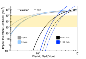
The thickness and electric field level of the gain layer is determined depending on the impact ionization coefficient. Figure 1 lists the impact ionization coefficients of Si and 4H-SiC from different models. Based on previous study of P-type Si-LGAD, the electric field is between for the thickness of gain layer [20]. Similarly, in terms of the gain layer with the thickness of , the impact ionization coefficient of the low gain region ranges from , as highlighted in the yellow band of Figure 1, the electric field is about for the 4H-SiC LGAD. To acquire the higher gain/E ratio, the N-type 4H-SiC LGAD is adopted in our work where the impact ionization of initial holes dominates the carrier multiplication.
To acquire enough initial e-h pairs, the thickness of the bulk layer should be considered in design of 4H-SiC LGAD. In our design, a 50 bulk layer is decided which would be ionized initial e-h pairs by MIP. After the multiplication of carries with gain, the collected charges is about 4 fC. However, to utilize the total 50 bulk layer, it should be depleted under an appropriate low voltage. So it demands the doping level of the bulk layer as low as possible. The high quality, low doping and thick 4H-SiC epitaxy are the main challenges of 4H-SiC LGAD. Fortunately, depending on our previous study, the high quality 100 4H-SiC epitaxy layer with the doping level has been achieved successfully in the PIN device to detect MIPs. Conservatively, the doping level of the bulk layer is determined to in the 4H-SiC LGAD design.
One of the significant operating conditions of LGAD is
| (1) |
where is operating voltage, is full depletion voltage and is breakdown voltage. And the device should have an appropriate gain between and . In our design, we demand the gain at and to guarantee the operating voltage range could be applied by the present source meter like Keithley 2410. Under those limitations, the thickness and doping level of 4H-SiC LGAD could be deduced analytically.
The is calculated by
| (2) |
where q is unit charge; and are depletion voltage of gain layer and bulk layer; and are doping level; and are thickness of corresponding layer. The is estimated if consider and that mentioned before. Then the the average electric field in gain layer could be deduced:
| (3) |
Consider the average electric field in gain layer is , the impact ionization coefficient of electron and hole could be calculated by different model. In our work, the Hatakeyama model[22] is applied because the anisotropy is considered. So the number of e-h pairs created by a single of initial e-h pair at position in the depleted gain layer is[23]
| (4) |
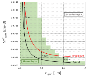
The breakdown condition is assumed to in N-type 4H-SiC LGAD. Consequently, the relation between and can be determined which shows in Figure 2 depends on Eq. 1-4 and other limitations mentioned in our design. The results in Figure 2 indicate the theoretical and values should be located in “allowed region” between the black line (Gain=1) and red line (Gain=). Some important information could be extracted in Figure 2 to guid the design of 4H-SiC LGAD: (1) The could not be larger than otherwise the device will be premature breakdown before full depletion; (2) In general, decreases with the thickness of . When is less than , decreases rapidly by nearly one order of magnitude with the increase of and gradually flattens when is greater than 0.5um. Therefore, the is not suggested due to high sensitive between the and ; (3) 1.0 thickness is reasonable but easily premature breakdown caused by the fluctuation of and in practical process. For a comprehensive consideration, the 0.5 thickness of gain layer is adopted in this work where the doping level between .
3 Simulation
To verify the results by analytical analysis in Sec. 2 and determine the specific doping level of gain layer , we simulate the characteristics of 4H-SiC LGAD with the help of TCAD (Technology Computer Aided Design) tools.
3.1 Configuration of physical parameters
In our simulation, the dielectric constant of 4H-SiC material is . The electron & hole effective mass and conduction band density-of-state models are from [24]. The parameters of the carrier mobility model with doping-dependence refer to [25, 26]. The impact ionization model uses Hatakeyama model [22]. The MIPs is simulated by heavy ion model of TCAD [27]. Finally, the wafer system of 4H-SiC has a 4∘ miscut angle in all simulations.
3.2 Structure
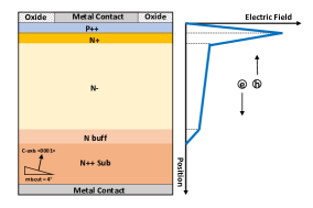
Depends on the analytical analysis in Sec. 2, a 2D 4H-SiC LGAD structure is designed (see Figure 3(a)) which has five 4H-SiC layers listed below:
-
1.
P++ : contact layer, 0.3, .
-
2.
N+ : gain layer, the thickness and doping level are studied in this work.
-
3.
N- : bulk layer, 50, .
-
4.
N buff : buff layer, 5.0, .
-
5.
N++ : substrate layer, 10, .
The width of the structure is 10 which is satisfied with 2D heavy ion simulation. Because of the “triangle” electric field between P++ layer and N+ layer, we address the structure like Figure 3(a) as Triangle-Type 4H-SiC LGAD. For comparative study, the same structure of 4H-SiC PIN is designed and the N+ gain layer is removed.
3.3 Simulated I-V and 1/C2-V
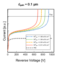
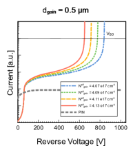
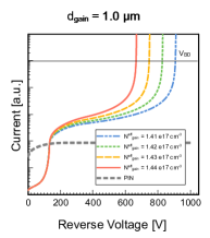
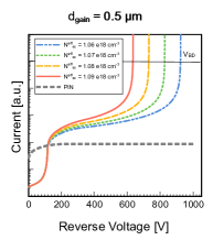
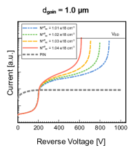
To determine the breakdown voltage for the Triangle-Type 4H-SiC LGAD, the I-V curves are simulated which is shown in Figure 4. As Figure 4Figure 4 show, for different gain layer doping levels, the breakdown voltages could be restrained in 500 V1000 V in our designs. Under this condition, the order of magnitude of is when and when . It agrees with the predication of analytical analysis in Figure 2. Compare with the fluctuation interval of related with between 500 V1000 V, the declining rate of is for , but increases to for . It also agrees with the analysis in Sec. 2 where the relevance is stronger between and for thinner . It should be noted that the leakage current of 4H-SiC LGAD at low voltages is smaller than PIN is caused by very small volume of depleted region when . However, the leakage current of all 4H-SiC LGAD designs are larger than PIN after full depletion. The gain of leakage current is times indicates the low gain is achieved.
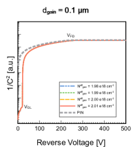
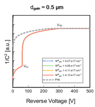
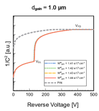
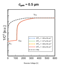
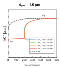
To determine the gain layer depletion voltage and full depletion voltage for the Triangle-Type 4H-SiC LGAD, the 1/C2-V curves are simulated which is shown in Figure 5. As Figure 5Figure 5 show, the influence for fluctuation of to could be neglected. For different gain layer doping levels, the of all 4H-SiC LGAD designs are smaller than 500 V that is satisfied with our demand referred in Sec. 3.4. Compare with the fluctuation interval of related with for different , the increases rapidly from 140 V for to 140 V for , although the has already decreased one order of magnitude. It indicates the thickness of gain layer is leading factor of in 4H-SiC LGAD.
3.4 Study of gain layer design
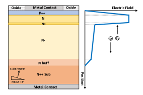
To control the electric field near the gain layer handily, another 4H-SiC LGAD structure is introduced which has an “trapezoid” electric field (See Figure 3(b)). As mentioned in Sec. 3.2, we address it as Trapezoid-Type 4H-SiC LGAD. Different with the Triangle-Type 4H-SiC LGAD has five layers, the Trapezoid-Type has six layers where another N+ layer called the electric field control layer which is inserted into the interface between the N gain layer and N- bulk layer. The profiles of each layer are listed below:
-
1.
P++ : contact layer, 0.3, .
-
2.
N : gain layer, . The thickness is studied in this work.
-
3.
N+ : electric field control layer, 0.1. The doping level are studied in this work.
-
4.
N- : bulk layer, 50, .
-
5.
N buff : buff layer, 5.0, .
-
6.
N++ : substrate layer, 10, .
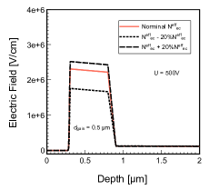
In the Trapezoid-Type 4H-SiC LGAD, the width of “trapezoid” electric field is dominated by the thickness of gain layer but the electric field level is controlled by the effective doping of electric field control layer . Figure 6 demonstrate the control action of electric field when the effective doping of electric field control layer changed %.
Similarly, the I-V and 1/C2-V curves are simulated for Trapezoid-Type 4H-SiC LGAD shown in Figure 7 and Figure 8. Only and are studied because the electric field layer is fixed to . Same with the Triangle-Type 4H-SiC LGAD, the breakdown voltages could also be restrained in 500 V1000 V and the full depletion voltage 500 V in our designs. It should be noted that another sudden-changing voltage is appeared in Figure 8 and Figure 8 due to electric field control layer is added.
3.5 Simulation of gain for MIP
To determine the gain factor when MIPs pass through the 4H-SiC LGAD, we use the heavy ion which has the same e-h pairs generation with MIP in 4H-SiC material to obtain the gain factor. The gain factor in this work is defined as:
| (5) |
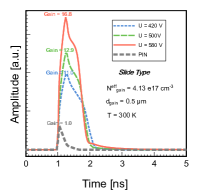
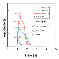
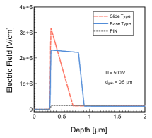
where is collected charges, is stimulated current by MIP and is collection time. Figure 9 and Figure 9 demonstrate the stimulated current by MIPs under different operating voltages. Compare with the stimulated current of PIN, The current gain for both type of 4H-SiC LGAD is when U=500 V. Under same operating voltage, the gain of Triangle-Type is higher than gain of Trapezoid-Type. It could be interpreted by using the profile of electric field shown in Figure 10, where the higher electric field peak for Triangle-Type dominates the gain factor although the Trapezoid-Type has higher average electric field . The electric field levels shown in Figure 10 agree with the predication in Figure 1. Based on simulation, we determine the electric field is for Triangle-Type and for Trapezoid-Type to a 4H-SiC LGAD with .
The time-response is described by the rising slope of stimulated current by MIP which is defined as , where the is the max value of stimulated current and is rising time. Figure 10 demonstrates the direct proportion with gain and the rising slope. And it indicates both types of 4H-SiC LGAD have the same time response for the same gain. Combined with the previous analysis that the Triangle-Type has a higher gain than Trapezoid-Type, the Triangle-Type is better for the application of fast MIP detection.
3.6 Efficiency of gain obtaining and stability
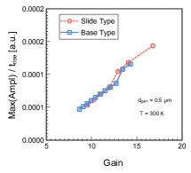
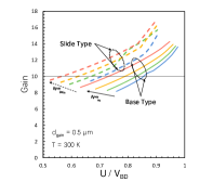
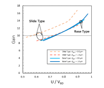
To compare the efficiency of gain obtaining for two types 4H-SiC LGAD, the relations between gain and the ratio are studied. Figure 11 shows the Triangle-Type 4H-SiC LGAD has higher efficiency of gain obtaining because it has a higher gain factor than Trapezoid-Type at the same value. But it also indicates the Triangle-Type is easier to reach the breakdown threshold, as reflected in the rapidly increasing of gain when . Contrarily, all of Trapezoid-Type 4H-SiC LGADs behave more stable even if the .
Another piece of evidence that indicates the stability of the Trapezoid-Type 4H-SiC LGAD is shown in Figure 11. When the thickness of the gain layer increases from to , the curves for Trapezoid-Type 4H-SiC LGAD are not changed that means the efficiency of gain obtaining do not rely on . For the Triangle-Type 4H-SiC LGAD, the gain factor decreases when the increases at the same value of . It indicates the thinner gain layer has higher efficiency of gain obtaining but more easily breakdown. So the Trapezoid-Type 4H-SiC LGAD is better if consider its stability and robustness.
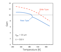
To investigate the temperature dependence and potential application in high temperature environment, the gain factors from T=300 K to T=500 K are simulated which are shown in Figure 11. Under the same operating voltage, the gain factor decreases with increasing of temperature. It is caused by the decreasing impact ionization coefficient depends on Hatakeyama model. The gain of both types are when the temperature below 400K.
4 Summary
Based on the analytical analysis in Sec. 2, we provide the policy to determine the doping level and thickness of gain layer in 4H-SiC LGAD. In our work, is adopted which has , bulk layer. The two types of LGAD structures are compared by simulation where the Triangle-Type has “triangle” electric field and Trapezoid-Type has “trapezoid” electric field. In the simulation, the gain is achieved when the operating voltage U between and . The Triangle-Type 4H-SiC LGAD is better for the application of fast MIP detection but also easily premature breakdown. The Triangle-Type 4H-SiC LGAD shows high stability and robustness but low efficiency of gain obtaining. It should be noticed that the simulation in this work is based on the specific configuration of physical parameters for 4H-SiC parameters. Different physical models impact the final results. Especially for the impact ionization coefficient predicated by different models[22, 21, 28, 29], the difference could be some magnitudes in 4H-SiC in our studied temperature range. So the study of practical devices is necessary in the future. The preliminary results of Trapezoid-Type 4H-SiC LGAD fabricated by Nanjing University (NJU)[30, 31] have already verified the process technology. Further study and optimization of NJU 4H-SiC LGAD are on going. We believe the more interesting results could be obtained for practical devices in the future. And it will help us to understand the impact ionization in the thin 4H-SiC layer like 4H-SiC LGAD structure.
Acknowledgment
This work has been supported by the National Natural Science Foundation of China (No. 11961141014), the State Key Laboratory of Particle Detection and Electronics (No. SKLPDE-ZZ-202218) under the CERN RD50 Collaboration framework.
References
- [1] ATLAS Collaboration. Technical Design Report for the ATLAS Inner Tracker Strip Detector, 2021. Technical report, CERN, Geneva, url:https://cds.cern.ch/record/2257755.
- [2] V. Sola et al. Ultra-Fast Silicon Detectors for 4D tracking. Journal of Instrumentation, 12(02), 2017. doi:10.1088/1748-0221/12/02/c02072.
- [3] G. Pellegrini et al. Technology developments and first measurements of Low Gain Avalanche Detectors (LGAD) for high energy physics applications. Nucl. Instrum. Methods A, 765, 2014. doi: 10.1016/j.nima.2014.06.008.
- [4] H. F. W. Sadrozinski et al. 4D tracking with ultra-fast silicon detectors. Rep. Prog. Phys., 81(2), 2018. doi: 10.1088/1361-6633/aa94d3.
- [5] V. Sola et al. First FBK production of 50 um ultra-fast silicon detectors. Nucl. Instrum. Methods A, 924, 2019. doi: 10.1016/j.nima.2018.07.060.
- [6] G. Giacomini et al. Development of a technology for the fabrication of Low-Gain Avalanche Diodes at BNL. Nucl. Instrum. Methods A, 934, 2019. doi: 10.1016/j.nima.2019.04.073.
- [7] K. Wu et al. Design of Low Gain Avalanche Detectors (LGAD) with 400 keV ion implantation energy for multiplication layer fabrication. Nucl. Instrum. Methods A, 984, 2020. doi:10.1016/j.nima.2020.164558.
- [8] Y.Y. Fan et al. Radiation hardness of the low gain avalanche diodes developed by NDL and IHEP in China. Nucl. Instrum. Methods A, 984, 2020. doi:10.1016/j.nima.2020.164608.
- [9] S. Xiao et al. Beam test results of NDL Low Gain Avalanche Detectors (LGAD). Nucl. Instrum. Methods A, 989, 2021. doi:10.1016/j.nima.2020.164956.
- [10] Y. Yang et al. Characterization of the first prototype NDL Low Gain Avalanche Detectors (LGAD). Nucl. Instrum. Methods A, 1011, 2021. doi:10.1016/j.nima.2021.165591.
- [11] Y. Tan et al. Radiation effects on NDL prototype LGAD sensors after proton irradiation. Nucl. Instrum. Methods A, 1010, 2021. doi:10.1016/j.nima.2021.165559.
- [12] G. Kramberger et al. Radiation effects in Low Gain Avalanche Detectors after hadronirradiations. Journal of Instrumentation, 10(07), 2015. doi: 10.1088/1748-0221/10/07/p07006.
- [13] M. Ferrero et al. Radiation resistant LGAD design. Nucl. Instrum. Methods A, 919, 2019. doi:10.1016/j.nima.2018.11.121.
- [14] Francesco Moscatelli et al. Measurements and simulations of charge collection efficiency of p+/n junction SiC detectors. Nucl. Instrum. Methods A, 546(1):218–221, 2005. Proceedings of the 6th International Workshop on Radiation Imaging Detectors.
- [15] T. Yang et al. Time resolution of the 4h-sic pin detector. Frontiers in Physics, 10, 2022. doi:10.3389/fphy.2022.718071.
- [16] Y. Tan et al. Timing Performance Simulation for 3D 4H-SiC Detector. Micromachines, 13(1), 2022. doi:10.3390/mi13010046.
- [17] R. Van Overstraeten et al. Measurement of the ionization rates in diffused silicon p-n junctions. Solid-State Electronics, 13(5), 1970. doi:10.1016/0038-1101(70)90139-5.
- [18] D.J. Massey et al. Temperature Dependence of Impact Ionization in Submicrometer Silicon Devices. IEEE Transactions on Electron Devices, 53(9), 2006. doi:10.1109/TED.2006.881010.
- [19] M. Mandurrino et al. Analysis and numerical design of Resistive AC-Coupled Silicon Detectors (RSD) for 4D particle tracking. Nucl. Instrum. Methods A, 959, 2020. doi:10.1016/j.nima.2020.163479.
- [20] T Yang and others. TCAD simulation and radiation damage modeling for low gain avalanche detector. 2021. arXiv:2106.15421.
- [21] W. S. Loh, , et al. Impact Ionization Coefficients in 4H-SiC. IEEE Transactions on Electron Devices, 55(8), 2008. doi:10.1109/TED.2008.926679.
- [22] T. Hatakeyama et al. Impact ionization coefficients of 4H silicon carbide. Applied Physics Letters, 85(8), 2004. doi:10.1063/1.1784520.
- [23] B. J. Baliga. Fundamentals of Power Semiconductor Devices. Fundamentals of Power Semiconductor Devices, 2019. doi:10.1007/978-3-319-93988-9.
- [24] G. Wellenhofer and U. Rössler. Global band structure and near-band edge states. Physica Status Solidi, 202(1):107–123, 1997. doi:10.1002/1521-3951.
- [25] W. J. Schaffer and others. Conductivity Anisotropy in Epitaxial 6H and 4H SiC. MRS Online Proceeding Library Archive, 339, 1994. doi:10.1557/PROC-339-595.
- [26] Tesfaye Ayalew. SiC Semiconductor Devices, Technology, Modeling, and Simulation. PhD thesis, Technishen Universiaet Wien, Austria, 2004.
- [27] Sentaurus Manual, https://www.synopsys.com.
- [28] H. Niwa et al. Impact Ionization Coefficients in 4H-SiC Toward Ultrahigh-Voltage Power Devices. IEEE Transactions on Electron Devices, 62(10):3326–3333, 2015. doi:10.1109/TED.2015.2466445.
- [29] S. Nida et al. High-Temperature Impact-Ionization Model for 4H-SiC. IEEE Transactions on Electron Devices, 66(4):1899–1904, 2019. doi:10.1109/TED.2019.2899285.
- [30] T Yang et al. Time resolution of 4H-SiC PIN and simulation of 4H-SiC LGAD, 2021. The 38th RD50 Workshop, url:https://indico.cern.ch/event/1029124/contributions/4411189/.
- [31] T Yang et al. Test results of the first 4H-SiC LGAD from NJU China, 2021. The 39th RD50 Workshop, url:https://indico.cern.ch/event/1074989/contributions/4601968/.