ampmtime \bstctlciteIEEEexample:BSTcontrol
Understanding RowHammer Under Reduced Wordline Voltage:
An Experimental Study Using Real DRAM Devices
Abstract
RowHammer is a circuit-level DRAM vulnerability, where repeatedly activating and precharging a DRAM row, and thus alternating the voltage of a row’s wordline between low and high voltage levels, can cause bit flips in physically nearby rows. Recent DRAM chips are more vulnerable to RowHammer: with technology node scaling, the minimum number of activate-precharge cycles to induce a RowHammer bit flip reduces and the RowHammer bit error rate increases. Therefore, it is critical to develop effective and scalable approaches to protect modern DRAM systems against RowHammer. To enable such solutions, it is essential to develop a deeper understanding of the RowHammer vulnerability of modern DRAM chips. However, even though the voltage toggling on a wordline is a key determinant of RowHammer vulnerability, no prior work experimentally demonstrates the effect of on the RowHammer vulnerability. Our work closes this gap in understanding.
This is the first work to experimentally demonstrate on 272 real DRAM chips that lowering reduces a DRAM chip’s RowHammer vulnerability. We show that lowering 1) increases the number of activate-precharge cycles needed to induce a RowHammer bit flip by up to with an average of across all tested chips and 2) decreases the RowHammer bit error rate by up to with an average of across all tested chips. At the same time, reducing marginally worsens a DRAM cell’s access latency, charge restoration, and data retention time within the guardbands of system-level nominal timing parameters for 208 out of 272 tested chips. We conclude that reducing is a promising strategy for reducing a DRAM chip’s RowHammer vulnerability without requiring modifications to DRAM chips.
1 Introduction
Manufacturing process technology scaling continuously increases DRAM storage density by reducing circuit component sizes and enabling tighter packing of DRAM cells. Such advancements reduce DRAM chip cost but worsen DRAM reliability [1, 2]. Kim et al. [3] show that modern DRAM chips are susceptible to a read disturbance effect, called RowHammer, where repeatedly activating and precharging a DRAM row (i.e., aggressor row) many times (i.e., hammering the aggressor row) can cause bit flips in physically nearby rows (i.e., victim rows) at consistently predictable bit locations [4, 3, 5, 6, 7, 8, 9, 10, 11, 12, 13, 14, 15].
Many works [16, 17, 18, 19, 20, 21, 22, 23, 24, 25, 26, 8, 27, 28, 29, 30, 31, 32, 33, 9, 34, 35, 36, 37, 38, 39, 40, 41, 42, 43, 44, 45, 46, 47, 48, 13, 12, 4, 14, 10, 15, 7, 11, 3, 6] demonstrate that RowHammer is a serious security vulnerability that can be exploited to mount system-level attacks, such as escalating privilege or leaking private data. To make matters worse, recent experimental studies on real DRAM chips [8, 9, 36, 37, 11, 3, 43, 12] find that the RowHammer vulnerability is more severe in newer DRAM chip generations. For example, 1) the minimum aggressor row activation count necessary to cause a RowHammer bit flip () is only 4.8K and 10K for some newer LPDDR4 and DDR4 DRAM chips (manufactured in 2019–2020), which is and lower than the of 69.2K for some older DRAM chips (manufactured in 2010–2013) [11]; and 2) the fraction of DRAM cells that experience a bit flip in a DRAM row () after hammering two aggressor rows for times is for some newer DRAM chips from 2019–2020, which is larger than that for some other older chips manufactured in 2016–2017 () [11]. As the RowHammer vulnerability worsens, ensuring RowHammer-safe operation becomes more expensive across a broad range of system-level design metrics, including performance overhead, energy consumption, and hardware complexity [49, 8, 9, 11, 50, 51, 12, 43, 52, 36].
To find effective and efficient solutions for RowHammer, it is essential to develop a deeper understanding of the RowHammer vulnerability of modern DRAM chips [12, 8, 9]. Prior works [3, 4, 8, 9, 15, 10, 7, 6, 12, 11] hypothesize that the RowHammer vulnerability originates from circuit-level interference between 1) wordlines that are physically nearby each other and 2) between a wordline and physically nearby DRAM cells. Existing circuit-level models [7, 10, 15] suggest that toggling of the voltage on a wordline is a key determinant of how much repeated aggressor row activations disturb physically nearby circuit components. However, it is still unclear 1) how the magnitude of the wordline voltage () affects modern DRAM chips’ RowHammer vulnerability and 2) whether it is possible to reduce RowHammer vulnerability by reducing , without significantly worsening other issues related to reliable DRAM operation. Therefore, our goal is to experimentally understand how affects RowHammer vulnerability and DRAM operation.
Our Hypothesis. We hypothesize that lowering can reduce RowHammer vulnerability without significantly impacting reliable DRAM operation. To test this hypothesis, we experimentally demonstrate how RowHammer vulnerability varies with by conducting rigorous experiments on 272 real DDR4 DRAM chips from three major DRAM vendors. To isolate the effect of and to avoid failures in DRAM chip I/O circuitry, we scale only and supply the rest of the DRAM circuitry using the nominal supply voltage ().
Key Findings. Our experimental results yield six novel observations about ’s effect on RowHammer (§5). Our key observation is that a DRAM chip’s RowHammer vulnerability reduces by scaling down : 1) increases by (), and 2) the caused by a RowHammer attack reduces by (), on average (at max) across all tested DDR4 DRAM chips.
To investigate the potential adverse effects of reducing on reliable DRAM operation, we conduct experiments using both real DDR4 DRAM chips and SPICE [53] simulations that measure how reducing affects a DRAM cells’ 1) row activation latency, 2) charge restoration process, and 3) data retention time. Our measurements yield nine novel observations (§6). We make two key observations: First, reduction only marginally worsens the access latency, charge restoration process, and data retention time of most DRAM chips: 208 out of 272 tested DRAM chips reliably operate using nominal timing parameters due to the built-in safety margins (i.e., guardbands) in nominal timing parameters that DRAM manufacturers already provide. Second, 64 DRAM chips that exhibit erroneous behavior at reduced can reliably operate using 1) a longer row activation latency, i.e., / for 48 / 16 chips (§6.1), 2) simple single-error-correcting codes [54] (§6.3), or 3) doubling the refresh rate only for of DRAM rows.
We make the following major contributions in this paper.
-
We present the first experimental RowHammer characterization study under reduced wordline voltage ().
-
Our experiments on 272 real DDR4 DRAM chips show that when a DRAM module is operated at a reduced , an attacker 1) needs to hammer a row in the module more times (by / ) to induce a bit flip, and 2) can cause fewer ( / ) RowHammer bit flips in the module (on average / at maximum across all tested modules).
-
We present the first experimental study of how reducing affects DRAM access latency, charge restoration process, and data retention time.
-
Our experiments on real DRAM chips show that reducing slightly worsens DRAM access latency, charge restoration process, and data retention time. Most (208 out of 272) DRAM chips reliably operate under reduced , while the remaining 64 chips reliably operate using increased row activation latency, simple error correcting codes, or doubling the refresh rate only for of the rows.
2 Background
We provide a high-level overview of DRAM design and operation as relevant to our work. For a more detailed overview, we refer the interested reader to prior works [55, 56, 57, 58, 59, 60, 61, 62, 63, 64, 65, 66, 67, 68, 69, 70, 3, 71, 72, 73, 74, 75, 76, 77, 78, 79].
2.1 DRAM Background
DRAM Organization. Fig. 1 illustrates a DRAM module’s hierarchical organization. At the lowest level of the hierarchy, a single DRAM cell comprises 1) a storage capacitor that stores a single bit of data encoded using the charge level in the capacitor and 2) an access transistor that is used to read from and write to the storage capacitor. The DRAM cell is connected to a bitline that is used to access the data stored in the cell and a wordline that controls access to the cell.
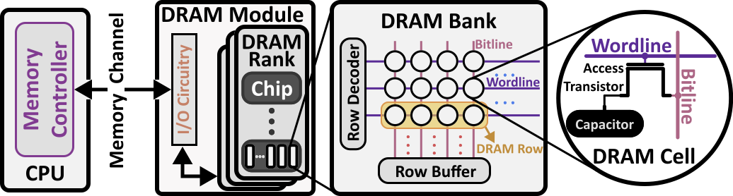
DRAM cells are organized as a two-dimensional array to form a bank. Each cell in a bank is addressed by its row and column. Each DRAM cell in a DRAM row is connected to a common wordline via its access transistor. A bitline connects a column of DRAM cells to a DRAM sense amplifier to read or write data. A row of sense amplifiers is called a row buffer. Multiple (e.g., 16 [80]) DRAM banks are put together to form a single DRAM chip. Multiple chips form a rank. Chips in a rank operate in lock-step such that each chip serves a portion of the data for each DRAM access. A DRAM module may have one or more ranks, communicating with the memory controller over the memory channel.
DRAM Operation. The memory controller services main memory requests using three key operations.
1) Row Activation. The memory controller sends an command along with a row address to a bank, and the DRAM chip asserts the corresponding wordline to activate the DRAM row. Asserting a wordline connects each cell capacitor in the activated row to its corresponding bitline, perturbing the bitline voltage. Then, the sense amplifier senses and amplifies the voltage perturbation until the cell charge is restored. The data is accessible when the bitline voltage is amplified to a certain level. The latency from the start of row activation until the data is reliably readable is called row activation latency (). A DRAM cell loses its charge during row activation, and thus its initial charge needs to be restored before the row is closed. The latency from the start of row activation until the completion of the DRAM cell’s charge restoration is called charge restoration latency (). DRAM manufacturers provide a built-in safety margin in the nominal timing parameters to account for the worst-case latency in and operations [58, 81, 60].
2) Read/Write. The memory controller sends a / command along with a column address to perform a read or write to the activated row in the DRAM bank. A command serves data from the row buffer to the memory channel. A command writes data into the row buffer, which subsequently modifies the data stored in the DRAM cell. The latency of performing a read/write operation is called column access latency ()/ column write latency ().
3) Precharge. The memory controller sends a command to an active bank. The DRAM chip de-asserts the active row’s wordline and precharges the bitlines to prepare the DRAM bank for a new row activation. The timing parameter for precharge is called precharge latency (), which is the latency between issuing a command and when the DRAM bank is ready for a new row activation.
DRAM Refresh. A DRAM cell inherently leaks charge and thus can retain data for only a limited amount of time, called data retention time. To prevent data loss due to such leakage, the memory controller periodically issues (refresh) commands that ensure every DRAM cell is refreshed at a fixed interval, called refresh window () (e.g., every [82, 80, 83] or [84]).
2.2 DRAM Voltage Control
Modern DRAM chips (e.g., DDR4 [80], DDR5 [83], GDDR5X [85], and GDDR6 [86] standard compliant ones) use two separate voltage rails: 1) supply voltage (), which is used to operate the core DRAM array and peripheral circuitry (e.g., the sense amplifiers, row/column decoders, precharge and I/O logic), and 2) wordline voltage (), which is exclusively used to assert a wordline during a DRAM row activation. is generally significantly higher (e.g., 2.5V [87, 88, 89, 90]) than (e.g., 1.25–1.5V [87, 88, 89, 90]) in order to ensure 1) full activation of all access transistors of a row when the wordline is asserted and 2) low leakage when the wordline is de-asserted. is internally generated from in older DRAM chips (e.g., DDR3 [82]). However, newer DRAM chips (e.g., DDR4 onwards [80, 83, 85, 86]) expose both and rails to external pins, allowing and to be independently driven with different voltage sources.
2.3 The RowHammer Vulnerability
Modern DRAM is susceptible to a circuit-level vulnerability known as RowHammer [4, 3, 5, 6, 7, 8, 9, 10, 11, 12, 13, 14, 15], where a cell’s stored data can be corrupted by repeatedly activating physically nearby (aggressor) rows. RowHammer results in unwanted software-visible bit flips and breaks memory isolation [3, 9, 8]. RowHammer poses a significant threat to system security, reliability, and DRAM technology scaling. First, RowHammer leads to data corruption, system crashes, and security attacks if not appropriately mitigated. Many prior works [16, 17, 18, 19, 20, 21, 22, 23, 24, 25, 26, 8, 27, 28, 29, 30, 31, 32, 33, 9, 34, 35, 36, 37, 38, 39, 40, 41, 42, 43, 44, 45, 46, 47, 48] show that RowHammer can be exploited to mount system-level attacks to compromise system security (e.g., to acquire root privileges or leak private data). Second, RowHammer vulnerability worsens as DRAM technology scales to smaller node sizes [8, 9, 36, 37, 11, 3, 43, 12]. This is because process technology shrinkage reduces the size of circuit elements, exacerbating charge leakage paths in and around each DRAM cell. Prior works [11, 36, 43, 12] experimentally demonstrate with modern DRAM chips that RowHammer is and will continue to be an increasingly significant reliability, security, and safety problem going forward [8, 9], given that the minimum aggressor row activation count necessary to cause a RowHammer bit flip () is only 4.8K in modern DRAM chips [11] and it continues to reduce.
We describe two major error mechanisms that lead to RowHammer, as explained by prior works [4, 7, 10, 15, 91, 6, 92]: 1) electron injection / diffusion / drift and 2) capacitive crosstalk. The electron injection / diffusion / drift mechanism creates temporary charge leakage paths that degrade the voltage of a cell’s storage capacitor [15, 10, 91, 6]. A larger voltage difference between a wordline and a DRAM cell or between two wordlines exacerbates the electron injection / diffusion / drift error mechanism. The capacitive crosstalk mechanism exacerbates charge leakage paths in and around a DRAM cell’s capacitor [15, 91, 4, 92] due to the parasitic capacitance between two wordlines or between a wordline and a DRAM cell.
2.4 Wordline Voltage’s Impact on DRAM Reliability
RowHammer. As explained in §2.3, a larger exacerbates both electron injection / diffusion / drift and capacitive crosstalk mechanisms. Therefore, we hypothesize that the RowHammer vulnerability of a DRAM chip increases as increases. Unfortunately, there is no prior work that tests this hypothesis and quantifies the effect of on real DRAM chips’ RowHammer vulnerability. §3 discusses this hypothesis in further detail, and §5 experimentally examines the effects of changing on the RowHammer vulnerability of real DRAM chips.
Row Activation and Charge Restoration. An access transistor turns on (off) when its gate voltage is higher (lower) than a threshold. An access transistor’s gate is connected to a wordline (Fig. 1) and driven by (ground) when the row is activated (precharged).111To increase DRAM cell retention time, modern DRAM chips may apply a negative voltage to the wordline [93, 94] when the wordline is not asserted. Doing so reduces the leakage current and this improves data retention. Between and ground, a larger access transistor gate voltage forms a stronger channel between the bitline and the capacitor. A strong channel allows fast DRAM row activation and full charge restoration. Based on these properties, we hypothesize that a larger provides smaller row activation latency and increased data retention time, leading to more reliable DRAM operation.222Increasing/decreasing does not affect the reliability of / and operations since the DRAM circuit components involved in these operations are powered using only . Unfortunately, there is no prior work that tests this hypothesis and quantifies ’s effect on real DRAM chips’ reliable operation (i.e., row activation and charge restoration characteristics). §6 studies the effect of reduced on DRAM operation reliability using both real-device characterizations and SPICE [53, 95] simulations.
3 Motivation
RowHammer is a critical vulnerability for modern DRAM-based computing platforms [4, 3, 6, 7, 8, 9, 10, 11, 12, 13, 14, 16, 5, 17, 18, 19, 21, 22, 23, 24, 25, 26, 27, 29, 30, 31, 32, 33, 34, 35, 36, 37, 38, 39, 40, 41, 42, 43, 44, 45, 46, 47, 28, 15, 48, 20]. Many prior works [5, 96, 97, 3, 98, 99, 100, 101, 102, 30, 103, 51, 50, 104, 105, 106, 107, 48, 108, 80, 65, 109, 91, 110, 111, 112, 52, 13, 113, 45, 114] propose RowHammer mitigation mechanisms that aim to prevent RowHammer bit flips. Unfortunately, RowHammer solutions need to consider a large number of design space constraints that include cost, performance impact, energy and power overheads, hardware complexity, technology scalability, security guarantees, and changes to existing DRAM standards and interfaces. Recent works [11, 51, 50, 12, 36, 43, 8, 49, 52, 9] suggest that many existing proposals may fall short in one or more of these dimensions. As a result, there is a critical need for developing better RowHammer mitigation mechanisms.
To enable more effective and efficient RowHammer mitigation mechanisms, it is critical to develop a comprehensive understanding of how RowHammer bit flips occur [12, 8, 9]. In this work, we observe that although the wordline voltage () is expected to affect the amount of disturbance caused by a RowHammer attack [3, 4, 8, 9, 15, 10, 7, 6, 12, 11, 14, 13], no prior work experimentally studies its real-world impact on a DRAM chip’s RowHammer vulnerability.333Both and can affect a DRAM chip’s RowHammer vulnerability. However, changing can negatively impact DRAM reliability in ways that are unrelated to RowHammer (e.g., I/O circuitry instabilities) because supplies power to all logic elements within the DRAM chip. In contrast, affects only the wordline voltage, so can influence RowHammer without adverse effects on unrelated parts of the DRAM chip. Therefore, our goal is to understand how affects RowHammer vulnerability and DRAM operation.
To achieve this goal, we start with the hypothesis that can be used to reduce a DRAM chip’s RowHammer vulnerability without impacting the reliability of normal DRAM operations. Reducing a DRAM chip’s RowHammer vulnerability via scaling has two key advantages. First, as a circuit-level RowHammer mitigation approach, scaling is complementary to existing system-level and architecture-level RowHammer mitigation mechanisms [5, 96, 97, 3, 98, 99, 100, 101, 102, 30, 103, 51, 50, 104, 105, 106, 107, 48, 108, 80, 65, 109, 91, 110, 111, 112, 52, 13, 113, 45, 114]. Therefore, scaling can be used alongside these mechanisms to increase their effectiveness and/or reduce their overheads. Second, scaling can be implemented with a fixed hardware cost for a given power budget, irrespective of the number and types of DRAM chips used in a system.
We test this hypothesis through the first experimental RowHammer characterization study under reduced . In this study, we test 272 real DDR4 DRAM chips from three major DRAM manufacturers. Our study is inspired by state-of-the-art analytical models for RowHammer, which suggest that the effect of RowHammer’s underlying error mechanisms depends on [15, 10, 7]. §5 reports our findings, which yield valuable insights into how impacts the circuit-level RowHammer characteristics of modern DRAM chips, both confirming our hypothesis and supporting scaling as a promising new dimension toward robust RowHammer mitigation.
4 Experimental Methodology
We describe our methodology for two analyses. First, we experimentally characterize the behavior of 272 real DDR4 DRAM chips from three major manufacturers under reduced in terms of RowHammer vulnerability (§4.2), row activation latency ()(§4.3), and data retention time (§4.4). Second, to verify our observations from real-device experiments, we investigate reduced ’s effect on both DRAM row activation and charge restoration using SPICE [95, 53] simulations (§4.5).
4.1 Real-Device Testing Infrastructure
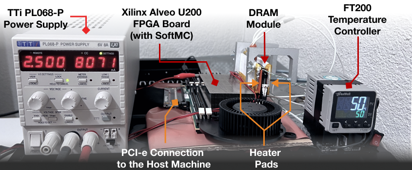
We conduct real-device characterization experiments using an infrastructure based on SoftMC [64, 115], the state-of-the-art FPGA-based open-source infrastructure for DRAM characterization. We extensively modify SoftMC to test modern DDR4 DRAM chips. Fig. 2 shows a picture of our experimental setup. We attach heater pads to the DRAM chips that are located on both sides of a DDR4 DIMM. We use a MaxWell FT200 PID temperature controller [116] connected to the heaters pads to maintain the DRAM chips under test at a preset temperature level with the precision of . We program a Xilinx Alveo U200 FPGA board [117] with the modified version of SoftMC. The FPGA board is connected to a host machine through a PCIe port for running our tests. We connect the DRAM module to the FPGA board via a commercial interposer board from Adexelec [118] with current measurement capability. The interposer board enforces the power to be supplied through a shunt resistor on the rail. We remove this shunt resistor to electrically disconnect the rails of the DRAM module and the FPGA board. Then, we supply power to the DRAM module’s power rail from an external TTi PL068-P power supply [119], which enables us to control at the precision of . We start testing each DRAM module at the nominal of . We gradually reduce with steps until the lowest at which the DRAM module can successfully communicate with the FPGA ().
To show that our observations are not specific to a certain DRAM architecture/process but rather common across different designs and generations, we test DDR4 DRAM modules from all three major manufacturers with different die revisions, purchased from the retail market. Table 1 provides the chip density, die revision (Die Rev.), chip organization (Org.), and manufacturing date of tested DRAM modules.444Die Rev. and Date columns are blank if undocumented. We report the manufacturing date of these modules in the form of . All tested modules are listed in Table 3 in Appendix A.
| Mfr. | #DIMMs | #Chips | Density | Die Rev. | Org. | Date |
| 1 | 8 | 4Gb | 8 | 48-16 | ||
| Mfr. A | 4 | 64 | 8Gb | B | 4 | 11-19 |
| (Micron) | 3 | 24 | 4Gb | F | 8 | 07-21 |
| 2 | 16 | 4Gb | 8 | |||
| 2 | 16 | 8Gb | B | 8 | 52-20 | |
| 1 | 8 | 8Gb | C | 8 | 19-19 | |
| Mfr. B | 3 | 24 | 8Gb | D | 8 | 10-21 |
| (Samsung) | 1 | 8 | 4Gb | E | 8 | 08-17 |
| 1 | 8 | 4Gb | F | 8 | 02-21 | |
| 2 | 16 | 8Gb | 8 | |||
| 2 | 16 | 16Gb | A | 8 | 51-20 | |
| Mfr. C | 3 | 24 | 4Gb | B | 8 | 02-21 |
| (SK Hynix) | 2 | 16 | 4Gb | C | 8 | |
| 3 | 24 | 8Gb | D | 8 | 48-20 |
Temperature. We conduct RowHammer and tests at and retention tests at to ensure both stable and representative testing conditions.555A recent work [12] shows a complex interaction between RowHammer and temperature, suggesting that one should repeat characterization at many different temperature levels to find the worst-case RowHammer vulnerability. Since such characterization requires many months-long testing time, we leave it to future work to study temperature, voltage, and RowHammer interaction in detail. We conduct tests at because is our infrastructure’s minimum stable temperature due to cooling limitations.666We do not repeat the tests at different temperature levels because prior work [60] shows small variation in with varying temperature. We conduct retention tests at to capture any effects of increased charge leakage [74] at the upper bound of regular operating temperatures [80].777DDR4 DRAM chips are refreshed at the nominal refresh rate when the chip temperature reaches [80]. Thus, we choose as a representative high temperature within the regular operating temperature range. For a detailed analysis of the effect of temperature on data retention in DRAM, we refer the reader to [120, 74, 77].
Disabling Sources of Interference. To understand fundamental device behavior in response to reduction, we make sure that is the only control variable in our experiments so that we can accurately measure the effects of on RowHammer, row activation latency (), and data retention time. To do so, we follow four steps, similar to prior rigorous RowHammer [11, 12], row activation latency [58, 81, 60], and data retention time [74, 77] characterization methods. First, we disable DRAM refresh to ensure no disturbance on the desired access pattern. Second, we ensure that during our RowHammer and experiments, no bit flips occur due to data retention failures by conducting each experiment within a time period of less than (i.e., much shorter than the nominal of ). Third, we test DRAM modules without error-correction code (ECC) support to ensure neither on-die ECC [121, 122, 123, 124, 125, 126, 127] nor rank-level ECC [32, 128] can affect our observations by correcting -reduction-induced bit flips. Fourth, we disable known on-DRAM-die RowHammer defenses (i.e., TRR [129, 83, 130, 88, 43, 36]) by not issuing refresh commands throughout our tests [36, 11, 12, 43] (as all TRR defenses require refresh commands to work).
Data Patterns. We use six commonly used data patterns [81, 60, 66, 67, 131, 11, 72, 132, 12, 3, 74]: row stripe (0xFF/0x00), checkerboard (0xAA/0x55), and thickchecker (0xCC/0x33). We identify the worst-case data pattern () for each row among these six patterns at nominal separately for each of RowHammer (§4.2), row activation latency ()(§4.3), and data retention time (§4.4) tests. We use each row’s corresponding for a given test, at reduced levels.
4.2 RowHammer Experiments
We perform multiple experiments to understand how affects the RowHammer vulnerability of a DRAM chip.
Metrics. We measure the RowHammer vulnerability of a DRAM chip using two metrics: 1) the minimum aggressor row activation count necessary to cause a RowHammer bit flip () and 2) the fraction of DRAM cells that experience a bit flip in a DRAM row ()caused by a double-sided RowHammer attack with a fixed hammer count of 300K per aggressor row.888We choose the 300K hammer count because 1) it is low enough to be used in a system-level RowHammer attack in a real system, and 2) it is high enough to provide us with a large number of bit flips to make meaningful observations in all DRAM modules we tested.
WCDP. We choose as the data pattern that causes the lowest . If there are multiple data patterns that cause the lowest , we choose the data pattern that causes the largest for the fixed hammer count of .999To investigate if changes with reduced , we repeat determination experiments for different values for 16 DRAM chips. We observe that changes for only of tested rows, causing less than deviation in for of the affected rows. We leave a detailed sensitivity analysis of to for future work.
RowHammer Tests. Alg. 1 describes the core test loop of each RowHammer test that we run. The algorithm performs a double-sided RowHammer attack on each row within a DRAM bank. A double-sided RowHammer attack activates the two attacker rows that are physically adjacent to a victim row (i.e., the victim row’s two immediate neighbors) in an alternating manner. We define hammer count () as the number of times each physically-adjacent row is activated. In this study, we perform double-sided attacks instead of single- [3] or many-sided attacks (e.g., as in TRRespass [36], U-TRR [43], and BlackSmith [44]) because a double-sided attack is the most effective RowHammer attack when no RowHammer defense mechanism is employed: it reduces and increases compared to both single- and many-sided attacks [12, 3, 11, 36, 43, 44]. Due to time limitations, 1) we test rows per DRAM module (four chunks of rows evenly distributed across a DRAM bank) and 2) we run each test ten times and record the smallest (largest) observed () to account for the worst-case.
Finding Physically Adjacent Rows. DRAM-internal address mapping schemes [37, 87] are used by DRAM manufacturers to translate logical DRAM addresses (e.g., row, bank, and column) that are exposed over the DRAM interface (to the memory controller) to physical DRAM addresses (e.g., physical location of a row). Internal address mapping schemes allow 1) post-manufacturing row repair techniques to repair erroneous DRAM rows by remapping these rows to spare rows and 2) DRAM manufacturers to organize DRAM internals in a cost-optimized way, e.g., by organizing internal DRAM buffers hierarchically [67, 133]. The mapping scheme can vary substantially across different DRAM chips [134, 37, 135, 136, 55, 67, 68, 3, 72, 74, 124, 12, 14, 137]. For every victim DRAM row we test, we identify the two neighboring physically-adjacent DRAM row addresses that the memory controller can use to access the aggressor rows in a double-sided RowHammer attack. To do so, we reverse-engineer the physical row organization using techniques described in prior works [11, 12].
4.3 Row Activation Latency () Experiments
We conduct experiments to find how a DRAM chip’s row activation latency () changes with reduced .
Metric. We measure the minimum time delay required ()between a row activation and the following read operation to ensure that there are no bit flips in the entire DRAM row.
WCDP. We choose as the data pattern that leads to the largest observed .
Tests. Alg. 2 describes the core test loop of each test that we run. The algorithm sweeps starting from the nominal of with steps of .101010Our version of SoftMC can send a DRAM command every due to the clock frequency limitations in the FPGA’s physical DRAM interface. We decrement (increment) by until we observe at least one (no) bit flip in the entire DRAM row in order to pinpoint . To test a DRAM row for a given , the algorithm 1) initializes the row with the row’s , 2) performs an access using the given for each column in the row and 3) checks if the access results in any bit flips. After testing each column in a DRAM row, the algorithm identifies the row’s as the minimum that does not cause any bit flip in the entire DRAM row. Due to time limitations, we 1) test the same set of rows as we use in RowHammer tests (§4.2) and 2) run each test ten times and record the largest for each row across all runs.111111To understand whether reliable DRAM row activation latency changes over time, we repeat these tests for 24 DRAM chips after one week, during which the chips are tested for RowHammer vulnerability. We observe that only of tested DRAM rows experience only a small variation () in . This result is consistent with results of prior works [81, 60, 69].
4.4 Data Retention Time Experiments
We conduct data retention time experiments to understand the effects of on DRAM cell data retention characteristics. We test the same set of DRAM rows as we use in RowHammer tests (§4.2) for a set of fixed refresh windows from to in increasing powers of two.
Metric. We measure the fraction of DRAM cells that experience a bit flip in a DRAM row (retention-) due to violating a DRAM row’s data retention time, using a reduced refresh rate.
WCDP. We choose as the data pattern which causes a bit flip at the smallest refresh window () among the six data patterns. If we find more than one such data pattern, we choose the one that leads to the largest for of .
Data Retention Time Tests. Alg. 3 describes how we perform data retention tests to measure retention- for a given and refresh rate. The algorithm 1) initializes a DRAM row with WCDP, 2) waits as long as the given refresh window, and 3) reads and compares the data in the DRAM row to the row’s initial data.
4.5 SPICE Model
To provide insights into our real-chip-based experimental observations about the effect of reduced on row activation latency and data retention time, we conduct a set of SPICE [95, 53] simulations to estimate the bitline and cell voltage levels during two relevant DRAM operations: row activation and charge restoration. To do so, we adopt and modify a SPICE model used in a relevant prior work [60] that studies the impact of changing (but not ) on DRAM row access and refresh operations. Table 2 summarizes our SPICE model, which we open-source [138]. We use LTspice [95] with the PTM transistor model [139, 140] and scale the simulation parameters according to the ITRS roadmap [141, 142].121212We do not expect SPICE simulation and real-world experimental results to be identical because a SPICE model cannot simulate a real DRAM chip’s exact behavior without proprietary design and manufacturing information. To account for manufacturing process variation, we perform Monte-Carlo simulations by randomly varying the component parameters up to for each simulation run. We run the simulation at levels from to with a step size of at 10K times, similar to prior works [65, 76].
| Component | Parameters |
|---|---|
| DRAM Cell | C: 16.8 fF, R: 698 |
| Bitline | C: 100.5 fF, R: 6980 |
| Cell Access NMOS | W: 55 nm, L: 85 nm |
| Sense Amp. NMOS | W: 1.3 um, L: 0.1 um |
| Sense Amp. PMOS | W: 0.9 um, L: 0.1 um |
4.6 Statistical Significance of Experimental Results
To evaluate the statistical significance of our methodology, we investigate the variation in our measurements by examining the coefficient of variation (CV) across ten iterations. CV is a standardized metric to measure the extent of variability in a set of measurements, in relation to the mean of the measurements. CV is calculated as the ratio of standard deviation over the mean value [143]. A smaller CV shows a smaller variation across measurements, indicating higher statistical significance. The coefficient of variation is 0.08, 0.13, and 0.24 for , , and percentiles of all of our experimental results, respectively.
5 RowHammer Under Reduced
We provide the first experimental characterization of how wordline voltage () affects the RowHammer vulnerability of a DRAM row in terms of 1) the fraction of DRAM cells that experience a bit flip in a DRAM row ()(§5.1) and 2) the minimum aggressor row activation count necessary to cause a RowHammer bit flip ()(§5.2). To conduct this analysis, we provide experimental results from 272 real DRAM chips, using the methodology described in §4.1 and §4.2.
5.1 Effect of on RowHammer BER
Fig. 3 shows the RowHammer a DRAM row experiences at a fixed hammer count of under different voltage levels, normalized to the row’s RowHammer at nominal (). Each line represents a different DRAM module. The band of shade around each line marks the confidence interval of the normalized value across all tested DRAM rows. We make Obsvs. 5.1 and 5.1 from Fig. 3.
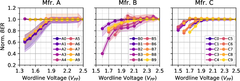
Observation 1. Fewer DRAM cells experience bit flips due to RowHammer under reduced wordline voltage.
We observe that RowHammer decreases as reduces in of tested rows across all tested modules. This reduction in reaches up to (B3 at ) with an average of (not shown in the figure) across all modules we test. We conclude that the disturbance caused by hammering a DRAM row becomes weaker, on average, with reduced .
Observation 2. In contrast to the dominant trend, reducing can sometimes increase .
We observe that increases in of tested rows with reduced by up to (B5 at ). We suspect that the increase we observe occurs due to a weakened charge restoration process rather than an actual increase in read disturbance (due to RowHammer). §6.3 analyzes the impact of reduced on the charge restoration process.
Variation in Reduction Across DRAM Rows. We investigate how reduction with reduced varies across DRAM rows. To do so, we measure reduction of each DRAM row at (§4.1). Fig. 4 shows a population density distribution of DRAM rows (y-axis) based on their at , normalized to their at the nominal level (x-axis), for each manufacturer. We make Obsv. 5.1 from Fig. 4.
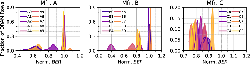
Observation 3. reduction with reduced varies across different DRAM rows and different manufacturers.
DRAM rows exhibit a large range of normalized values (0.43–1.11, 0.33–1.03, and 0.74–0.94 in chips from Mfrs. A, B, and C, respectively). reduction also varies across different manufacturers. For example, reduces by more than for all DRAM rows of Mfr. C, while variation with reduced is smaller than in of the rows of Mfr. A.
5.2 Effect of on
Fig. 5 shows the a DRAM row exhibits under different voltage levels, normalized to the row’s at nominal (). Each line represents a different DRAM module. The band of shade around each line marks the confidence interval of the normalized values across all tested DRAM rows in the module. We make Obsvs. 5.2 and 5.2 from Fig. 3.
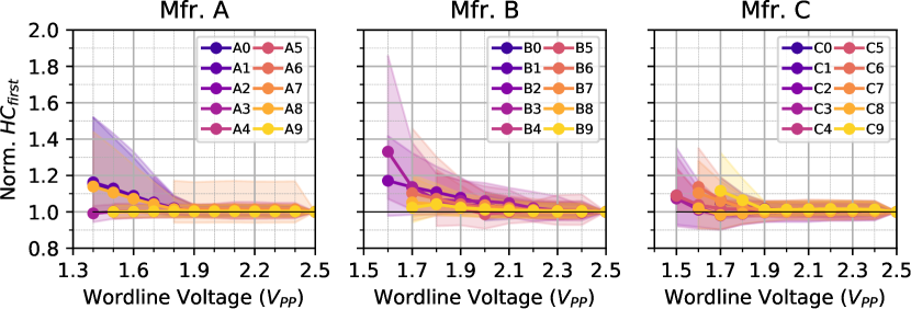
Observation 4. DRAM cells experience RowHammer bit flips at higher hammer counts under reduced wordline voltage.
We observe that of a DRAM row increases as reduces in of tested rows across all tested modules. This increase in reaches up to (B3 at ) with an average of (not shown in the figure) across all tested modules. We conclude that the disturbance caused by hammering a DRAM row becomes weaker with reduced .
Observation 5. In contrast to the dominant trend, reducing can sometimes cause bit flips at lower hammer counts.
We observe that reduces in of tested rows with reduced by up to (C8 at =). Similar to Obsv. 5.1, we suspect that this behavior is caused by the weakened charge restoration process (see §6.3).
Variation in Increase Across DRAM Rows. We investigate how increase varies with reduced across DRAM rows. To do so, we measure increase of each DRAM row at (§4.1). Fig. 6 shows a population density distribution of DRAM rows (y-axis) based on their at , normalized to their at the nominal level (x-axis), for each manufacturer. We make Obsv. 5.2 from Fig. 6.
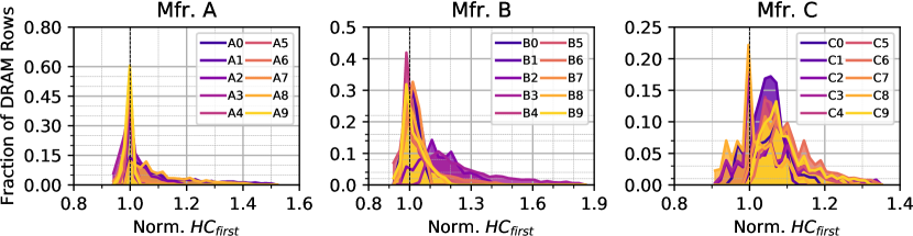
Observation 6. increase with reduced varies across different DRAM rows and different manufacturers.
DRAM rows in chips from the same manufacturer exhibit a large range of normalized values (0.94–1.52, 0.92–1.86, and 0.91–1.35 for Mfrs. A, B, and C, respectively). increase also varies across different manufacturers. For example, increases with reduced for of DRAM rows in modules from Mfr. C, while of DRAM rows exhibit this behavior in modules from Mfr. A.
Based on Obsvs. 5.2–5.2, we conclude that a DRAM row’s tends to increase with reduced , while both the amount and the direction of change in varies across different DRAM rows and manufacturers.
Summary of Findings. Based on our analyses on both and , we conclude that a DRAM chip’s RowHammer vulnerability can be reduced by operating the chip at a level that is lower than the nominal value.
6 DRAM Reliability Under Reduced
To investigate the effect of reduced on reliable DRAM operation, we provide the first experimental characterization of how affects the reliability of three -related fundamental DRAM operations: 1) DRAM row activation (§6.1), 2) charge restoration (§6.2), and 3) DRAM refresh (§6.3). To conduct these analyses, we provide both 1) experimental results from real DRAM devices, using the methodology described in §4.1, §4.3, and §4.4 and 2) SPICE simulation results, using the methodology described in §4.5.
6.1 DRAM Row Activation Under Reduced
Motivation. DRAM row activation latency () should theoretically increase with reduced (§2.2). We investigate how of real DRAM chips change with reduced .
Novelty. We provide the first experimental analysis of the isolated impact of on activation latency. Prior work [60] tests DDR3 DRAM chips under reduced supply voltage (), which may or may not change internally-generated level. In contrast, we modify only wordline voltage () without modifying to avoid the possibility of negatively impacting DRAM reliability due to I/O circuitry instabilities (§2.2).
Experimental Results. Fig. 7 demonstrates the variation in (§4.3) on the y-axis under reduced on the x-axis, across 30 DRAM modules. We annotate the nominal value () [80] with a black horizontal line. We make Obsv. 6.1 from Fig. 7.
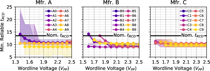
Observation 7. Reliable row activation latency generally increases with reduced . However, 208 (25) out of 272 (30) DRAM chips (modules) complete row activation before the nominal activation latency.
The minimum reliable activation latency () increases with reduced across all tested modules. exceeds the nominal of for only 5 of 30 tested modules (A0–A2, B2, and B5). Among these, modules from Mfr. A and B contain 16 and 8 chips per module. Therefore, we conclude that 208 of 272 tested DRAM chips do not experience bit flips when operated using nominal . We observe that since increases with reduced , the available guardband reduces by with reduced , on average across all DRAM modules that reliably work with nominal . We also observe that the three and two modules from Mfrs. A and B, which exhibit values larger than the nominal , reliably operate when we use a of and , respectively.
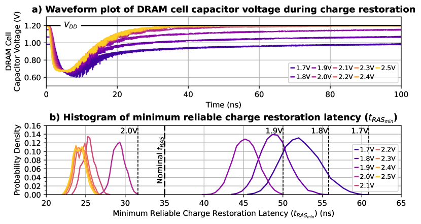
To verify our experimental observations and provide a deeper insight into the effect of on activation latency, we perform SPICE simulations (as described in §4.5). Fig. 8a shows a waveform of the bitline voltage during the row activation process. The time in the x-axis starts when an activation command is issued. Each color corresponds to the bitline voltage at a different level. We annotate the bitline’s supply voltage () and the voltage threshold that the bitline voltage should exceed for the activation to be reliably completed (). We make Obsv. 6.1 from Fig. 8a.
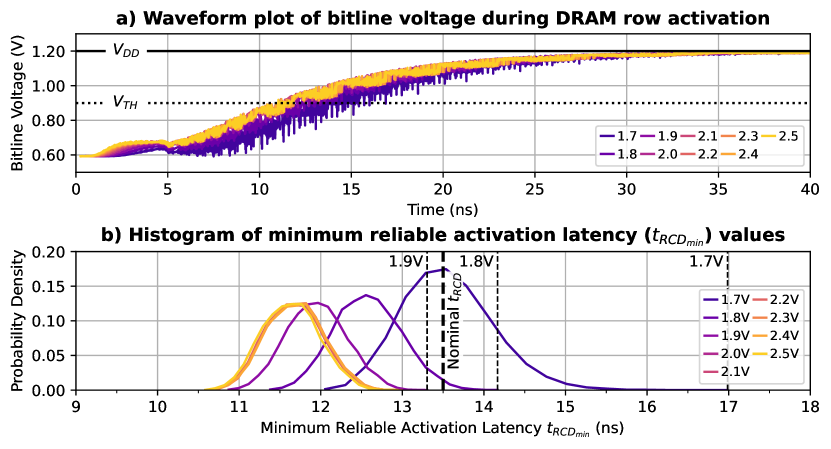
Observation 8. Row activation successfully completes under reduced with an increased activation latency.
Fig. 8a shows that, as decreases, the bitline voltage takes longer to increase to , resulting in a slower row activation. For example, increases from to (on average across Monte-Carlo simulation iterations) when is reduced from to . This happens due to two reasons. First, a lower creates a weaker channel in the access transistor, requiring a longer time for the capacitor and bitline to share charge. Second, the charge sharing process (0– in Fig. 8a) leads to a smaller change in bitline voltage when is reduced due to the weakened charge restoration process that we explain in §6.2.
Fig. 8b shows the probability density distribution of values under reduced across a total of Monte-Carlo simulation iterations for different levels (color-coded). Vertical lines annotate the worst-case reliable values across all iterations of our Monte-Carlo simulation (§4.5) for different levels. We make Obsv. 6.1 from Fig. 8b.
Observation 9. SPICE simulations agree with our activation latency-related observations based on experiments on real DRAM chips: increases with reduced .
We analyze the variation in 1) the probability density distribution of , and 2) the worst-case (largest) reliable value when is reduced. Fig. 8b shows that the probability density distribution of both shifts to larger values and becomes wider with reduced . The worst-case (largest) increases from to , , and when is reduced from to , and , respectively.131313SPICE simulation results do not show reliable operation when , yet real DRAM chips do operate reliably as we show in §6.1 and §6.3. For a realistic nominal value of , ’s guardband reduces from to as reduces from to . As §4.5 explains, SPICE simulation results do not exactly match measured real-device characteristics (shown in Obsv. 6.1) because a SPICE model cannot simulate a real DRAM chip’s exact behavior without proprietary design and manufacturing information.
From Obsvs. 6.1–6.1, we conclude that 1) the reliable row activation latency increases with reduced , 2) the increase in reliable row activation latency does not immediately require increasing the nominal , but reduces the available guardband by for 208 out of 272 tested chips, and 3) observed bit flips can be eliminated by increasing to and for erroneous modules from Mfrs. A and B.
6.2 DRAM Charge Restoration Under Reduced
Motivation. A DRAM cell’s charge restoration process is affected by because, similar to the row activation process, a DRAM cell capacitor’s charge is restored through the channel formed in the access transistor, which is controlled by the wordline. Due to access transistor’s characteristics, reducing without changing reduces gate-to-source voltage () and forms a weaker channel. To understand the impact of reduction on the charge restoration process, we investigate how charge restoration of a DRAM cell varies with reduced .
Experimental Results. Since our FPGA infrastructure cannot probe a DRAM cell capacitor’s voltage level, we conduct this study in our SPICE simulation environment (§4.5). Fig. 9a shows the waveform plot of capacitor voltage (y-axis) over time (x-axis), following a row activation event (at t=0). Fig. 9b shows the probability density distribution (y-axis) of the minimum latency required () to reliably complete the charge restoration process on the x-axis under different levels. We make Obsvs. 6.2 and 6.2 from Fig. 9a and 9b.
Observation 10. A DRAM cell’s capacitor voltage can saturate at a lower voltage level when is reduced.
We observe that a DRAM cell capacitor’s voltage saturates at () when is or higher. However, the cell capacitor’s voltage saturates at a lower voltage level by , , and when is , , and , respectively. This happens because the access transistor turns off when the voltage difference between its gate and source is smaller than a threshold level. For example, when is set to , the access transistor allows charge restoration until the cell voltage reaches . When the cell voltage reaches this level, the voltage difference between the gate () and the source () is not large enough to form a strong channel, causing the cell voltage to saturate at . This reduction in voltage can potentially 1) increase the row activation latency () and 2) reduce the cell’s retention time. We 1) already account for reduced saturation voltage’s effect on in §6.1 and 2) investigate its effect on retention time in §6.3.
Observation 11. The increase in a DRAM cell’s charge restoration latency with reduced can increase the timing parameter, depending on the level.
Similar to the variation in values that we discuss in Obsv. 6.1, the probability density distribution of values also shifts to larger values (i.e., exceeds the nominal value when is lower than 2.0V) and becomes wider as reduces. This happens as a result of reduced cell voltage, weakened channel in the access transistor, and reduced voltage level at the end of the charge sharing process, as we explain in Obsv. 6.1.
From Obsvs. 6.2 and 6.2, we conclude that reducing can negatively affect the charge restoration process. Reduced ’s negative impact on charge restoration can potentially be mitigated by leveraging the guardbands in DRAM timing parameters [58, 72, 81, 60, 69] and using intelligent DRAM refresh techniques, where a partially restored DRAM row can be refreshed more frequently than other rows, so that the row’s charge is restored before it experiences a data retention bit flip [144, 75, 145]. We leave exploring such solutions to future work.
6.3 DRAM Row Refresh Under Reduced
Motivation. §6.2 demonstrates that the charge restored in a DRAM cell after a row activation can be reduced as a result of reduction. This phenomenon is important for DRAM-based memories because reduced charge in a cell might reduce a DRAM cell’s data retention time, causing retention bit flips if the cell is not refreshed more frequently. To understand the impact of reduction on real DRAM chips, we investigate the effect of reduced on data retention related bit flips using the methodology described in §4.4.
Novelty. This is the first work that experimentally analyzes the isolated impact of on DRAM cell retention times. Prior work [60] tests DDR3 DRAM chips under reduced , which may or may not change the internally-generated level.
Experimental Results. Fig. 10 demonstrates reduced ’s effect on data retention on real DRAM chips. Fig. 10a shows how the data retention (y-axis) changes with increasing refresh window (log-scaled in x-axis) for different levels (color-coded). Each curve in Fig. 10a shows the average across all DRAM rows, and error bars mark the confidence interval. The x-axis starts from because we do not observe any bit flips at values smaller than . To provide deeper insight into reduced ’s effect on data retention , Fig. 10b demonstrates the population density distribution of data retention across tested rows for a of . Dotted vertical lines mark the average across rows for each level. We make Obsvs. 6.3 and 6.3 from Fig. 10.
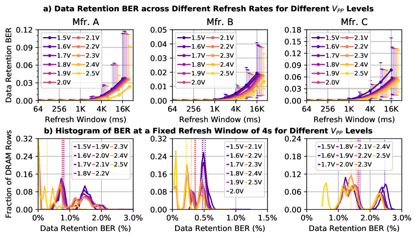
Observation 12. More DRAM cells tend to experience data retention bit flips when is reduced.
Fig. 10a shows that data retention curve is higher (e.g., dark-purple compared to yellow) for smaller levels (e.g., compared to ). To provide a deeper insight, Fig. 10b shows that average data retention across all tested rows when = increases from , , and for a of to , , and for a of for Mfrs. A, B, and C, respectively. We hypothesize that this happens because of the weakened charge restoration process with reduced (§6.2).
Observation 13. Even though DRAM cells experience retention bit flips at smaller retention times when is reduced, 23 of 30 tested modules experience no data retention bit flips at the nominal refresh window ().
Data retention is very low at the of even for a of . We observe that no DRAM module from Mfr. A exhibits a data retention bit flip at the , and only three and four modules from Mfrs. B (B6, B8, and B9) and C (C1, C3, C5, and C9) experience bit flips across all 30 DRAM modules we test.
We investigate the significance of the observed data retention bit flips and whether it is possible to mitigate these bit flips using error correcting codes (ECC) [54] or other existing methods to avoid data retention bit flips (e.g., selectively refreshing a small fraction of DRAM rows at a higher refresh rate [144, 75, 145]). To do so, we analyze the nature of data retention bit flips when each tested module is operated at the module’s for two values: and , which are the smallest refresh windows that yield non-zero BER for different DRAM modules.
To evaluate whether data retention bit flips can be avoided using ECC, we assume a realistic data word size of 64 bits [32, 128, 125, 124, 123, 137, 127]. We make Obsv. 6.3 from this analysis.
Observation 14. Data retention errors can be avoided using simple single error correcting codes at the smallest that yields non-zero .
We observe that no 64-bit data word contains more than one bit flip for the smallest that yield non-zero . We conclude that simple single error correction double error detection (SECDED) ECC can correct all erroneous data words.
To evaluate whether data retention bit flips can be avoided by selectively refreshing a small fraction of DRAM rows, we analyze the distribution of these bit flips across different DRAM rows. Fig. 11a (Fig. 11b) shows the distribution of DRAM rows that experience a data retention bit flip when is () but not at a smaller , based on their data retention bit flip characteristics. The x-axis shows the number of 64-bit data words with one bit flip in a DRAM row. The y-axis shows the fraction of DRAM rows in log-scale, exhibiting the behavior, specified in the x-axis for different manufacturers (color-coded). We make Obsv. 6.3 from Fig. 11.
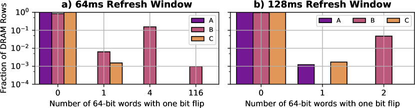
Observation 15. Only a small fraction ( / ) of DRAM rows contain erroneous data words at the smallest ( / ) that yields non-zero .
Fig. 11a shows that modules from Mfr. A do not exhibit any bit flips when is , while and of DRAM rows in modules from Mfrs. B and C exhibit four and one 64-bit words with a single bit flip, respectively; and of DRAM rows from Mfr. B contain 116 data words with one bit flip. Fig. 11b shows that , , and of rows from Mfrs. A, B, and C contain 1, 2, and 1 erroneous data words, respectively, when the refresh window is . We conclude that all of these data retention bit flips can be avoided by doubling the refresh rate141414We test our chips at fixed refresh rates in increasing powers of two (§4.4). Therefore, our experiments do not capture whether eliminating a bit flip is possible by increasing the refresh rate by less than . We leave a finer granularity data retention time analysis to future work. only for / of DRAM rows [144, 75, 145] when is / .
From Obsvs. 6.3–6.3, we conclude that a DRAM row’s data retention time can reduce when is reduced. However, 1) most of (i.e., 23 out of 30) tested modules do not exhibit any bit flips at the nominal of and 2) bit flips observed in seven modules can be mitigated using existing SECDED ECC [54] or selective refresh methods [144, 75, 145].
7 Limitations of Wordline Voltage Scaling
We highlight four key limitations of wordline voltage scaling and our experimental characterization.
First, in our experiments, we observe that none of the tested DRAM modules reliably operate at a lower than a certain voltage level, called . This happens because an access transistor cannot connect the DRAM cell capacitor to the bitline when the access transistor’s gate-to-source voltage difference is not larger than the transistor’s threshold voltage. Therefore, each DRAM chip has a minimum level at which it can reliably operate (e.g., lowest at for A0 and highest at for A5). With this limitation, we observe / average increase / reduction in / across all tested DRAM chips at their respective levels. A DRAM chip’s RowHammer vulnerability can potentially reduce further if access transistors are designed to operate at smaller levels.
Second, we cannot investigate the root cause of all results we observe since 1) DRAM manufacturers do not describe the exact circuit design details of their commodity DRAM chips [127, 14, 36, 137] and 2) our infrastructure’s physical limitations prevent us from observing a DRAM chip’s exact internal behavior (e.g., it is not possible to directly measure a cell’s capacitor voltage).
Third, this paper does not thoroughly analyze the three-way interaction between , temperature, and RowHammer. There is already a complex two-way interaction between RowHammer and temperature, requiring studies to test each DRAM cell at all allowed temperature levels [12]. Since a three-way interaction study requires even more characterization that would take several months of testing time, we leave it to future work to study the interaction between , temperature, and RowHammer.
Fourth, we experimentally demonstrate that the RowHammer vulnerability can be mitigated by reducing at the cost of a average reduction in the guardband of tested DRAM chips. Although reducing the guardband can hurt DRAM manufacturing yield, we leave studying reduction’s effect on yield to future work because we do not have access to DRAM manufacturers’ proprietary yield statistics.
8 Key Takeaways
We summarize the key findings of our experimental analyses of the wordline voltage ()’s effect on the RowHammer vulnerability and reliable operation of modern DRAM chips. From our new observations, we draw two key takeaways.
Takeaway 1: Effect of on RowHammer. We observe that scaling down reduces a DRAM chip’s RowHammer vulnerability, such that RowHammer decreases by (up to ) and increases by (up to ) on average across all DRAM rows. Only and of DRAM rows exhibit opposite and trends, respectively (§5.1 and §5.2).
Takeaway 2: Effect of on DRAM reliability. We observe that reducing 1) reduces the existing guardband for row activation latency by on average across tested chips and 2) causes DRAM cell charge to saturate at instead of () (§6.2), leading , , and of DRAM rows to experience SECDED ECC-correctable data retention bit flips at the nominal refresh window of in DRAM modules from Mfrs. A, B, and C, respectively (§6.3).
Finding Optimal Wordline Voltage. Our two key takeaways suggest that reducing RowHammer vulnerability of a DRAM chip via reduction can require 1) accessing DRAM rows with a slightly larger latency, 2) employing error correcting codes (ECC), or 3) refreshing a small subset of rows at a higher refresh rate. Therefore, one can define different Pareto-optimal operating conditions for different performance and reliability requirements. For example, a security-critical system can choose a lower to reduce RowHammer vulnerability, whereas a performance-critical and error-tolerant system might prefer lower access latency over higher RowHammer tolerance. DRAM designs and systems that are informed about the tradeoffs between , access latency, and retention time can make better-informed design decisions (e.g., fundamentally enable lower access latency) or employ better-informed memory controller policies (e.g., using longer , employing SECDED ECC, or doubling the refresh rate only for a small fraction of rows when the chip operates at reduced ). We believe such designs are important to explore in future work. We hope that the new insights we provide can lead to the design of stronger DRAM-based systems against RowHammer along with better-informed DRAM-based system designs.
9 Related Work
To our knowledge, this is the first work that experimentally studies how reducing wordline voltage affects a real DRAM chip’s 1) RowHammer vulnerability, 2) row activation latency, 3) charge restoration process, and 4) data retention time. We divide prior work into three categories: 1) explorations of reduced-voltage DRAM operation, 2) experimental characterization studies of the RowHammer vulnerability of real DRAM chips, and 3) RowHammer attacks and defenses.
Reduced-Voltage DRAM Operation. Prior works [146, 147, 60] propose operating DRAM with reduced to improve energy efficiency. [146] and [147] propose dynamic voltage and frequency scaling (DVFS) for DRAM chips and [146] provides results in a real system. [60] proposes to scale down without reducing DRAM chip frequency. To do so, [60] experimentally demonstrates the interaction between and DRAM row access latency in real DDR3 DRAM chips. These three works neither focus on the RowHammer vulnerability nor distinguish between and . Unlike these works, we focus on the impact of (isolated from ) on RowHammer and reliable operation characteristics of real DDR4 DRAM chips.
Experimental RowHammer Characterization. Prior works extensively characterize the RowHammer vulnerability in real DRAM chips[12, 43, 11, 3, 6, 36]. These works experimentally demonstrate (using real DDR3, DDR4, and LPDDR4 DRAM chips how) a DRAM chip’s RowHammer vulnerability varies with 1) DRAM refresh rate [43, 36, 3], 2) the physical distance between aggressor and victim rows [3, 11], 3) DRAM generation and technology node [12, 3, 11, 43], 4) temperature [12, 6], 5) the time the aggressor row stays active [12, 6], and 6) physical location of the victim DRAM cell [12]. None of these works analyze how reduced affects RowHammer vulnerability in real DRAM chips. Our characterization study furthers the analyses in these works by uncovering new insights into RowHammer behavior and DRAM operation.
RowHammer Attacks and Defenses. Many prior works [16, 17, 18, 19, 20, 21, 22, 23, 24, 25, 26, 8, 27, 28, 29, 30, 31, 32, 33, 9, 34, 35, 36, 37, 38, 39, 40, 41, 42, 43, 44, 45, 46, 47, 48, 13, 12, 4, 14, 10, 15, 7, 11, 3, 6] show that RowHammer can be exploited to mount system-level attacks to compromise system security and safety (e.g., to acquire root privileges or leak private data). To protect against these attacks, many prior works [5, 96, 97, 3, 98, 99, 100, 101, 102, 30, 103, 51, 50, 104, 105, 106, 107, 48, 108, 80, 65, 109, 91, 110, 111, 112, 52, 13, 113, 45, 114] propose RowHammer mitigation mechanisms that prevent RowHammer bit flips from compromising a system. The novel observations we make in this work can be leveraged to reduce RowHammer vulnerability and complement existing RowHammer defense mechanisms, further increasing their effectiveness and reducing their overheads.
10 Conclusion
We present the first experimental RowHammer characterization study under reduced wordline voltage (). Our results, using 272 real DDR4 DRAM chips from three major manufacturers, show that RowHammer vulnerability can be reduced by reducing . Using real-device experiments and SPICE simulations, we demonstrate that although the reduced slightly worsens DRAM access latency, charge restoration process and data retention time, most of (208 out of 272) tested chips reliably work under reduced leveraging already existing guardbands of nominal timing parameters and employing existing ECC or selective refresh techniques. Our findings provide new insights into the increasingly critical RowHammer problem in modern DRAM chips. We hope that they lead to the design of systems that are more robust against RowHammer attacks.
Acknowledgments
We thank our shepherd Karthik Pattabiraman and the anonymous reviewers of DSN 2022 for valuable feedback. We thank the SAFARI Research Group members for valuable feedback and the stimulating intellectual environment they provide. We acknowledge the generous gifts provided by our industrial partners, including Google, Huawei, Intel, Microsoft, and VMware, and support from the Microsoft Swiss Joint Research Center.
References
- [1] O. Mutlu, “Memory Scaling: A Systems Architecture Perspective,” in IMW, 2013.
- [2] J. Meza, Q. Wu, S. Kumar, and O. Mutlu, “Revisiting Memory Errors in Large-Scale Production Data Centers: Analysis and Modeling of New Trends from the Field,” in DSN, 2015.
- [3] Y. Kim, R. Daly, J. Kim, C. Fallin, J. H. Lee, D. Lee, C. Wilkerson, K. Lai, and O. Mutlu, “Flipping Bits in Memory Without Accessing Them: An Experimental Study of DRAM Disturbance Errors,” in ISCA, 2014.
- [4] M. Redeker, B. F. Cockburn, and D. G. Elliott, “An Investigation into Crosstalk Noise in DRAM Structures,” in MTDT, 2002.
- [5] B. Aichinger, “DDR Memory Errors Caused by Row Hammer,” in HPEC, 2015.
- [6] K. Park, C. Lim, D. Yun, and S. Baeg, “Experiments and Root Cause Analysis for Active-Precharge Hammering Fault in DDR3 SDRAM under 3xnm Technology,” Microelectronics Reliability, 2016.
- [7] K. Park, D. Yun, and S. Baeg, “Statistical Distributions of Row-Hammering Induced Failures in DDR3 Components,” Microelectronics Reliability, 2016.
- [8] O. Mutlu, “The RowHammer Problem and Other Issues We May Face as Memory Becomes Denser,” in DATE, 2017.
- [9] O. Mutlu and J. S. Kim, “RowHammer: A Retrospective,” TCAD, 2019.
- [10] T. Yang and X.-W. Lin, “Trap-Assisted DRAM Row Hammer Effect,” EDL, 2019.
- [11] J. S. Kim, M. Patel, A. G. Yağlıkçı, H. Hassan, R. Azizi, L. Orosa, and O. Mutlu, “Revisiting RowHammer: An Experimental Analysis of Modern Devices and Mitigation Techniques,” in ISCA, 2020.
- [12] L. Orosa, A. G. Yağlıkçı, H. Luo, A. Olgun, J. Park, H. Hassan, M. Patel, J. S. Kim, and O. Mutlu, “A Deeper Look into RowHammer’s Sensitivities: Experimental Analysis of Real DRAM Chips and Implications on Future Attacks and Defenses,” in MICRO, 2021.
- [13] M. Qureshi, “Rethinking ECC in the Era of Row-Hammer,” DRAMSec, 2021.
- [14] S. Saroiu, A. Wolman, and L. Cojocar, “The Price of Secrecy: How Hiding Internal DRAM Topologies Hurts Rowhammer Defenses,” in IRPS, 2022.
- [15] A. J. Walker, S. Lee, and D. Beery, “On DRAM RowHammer and the Physics on Insecurity,” IEEE TED, 2021.
- [16] M. Seaborn and T. Dullien, “Exploiting the DRAM Rowhammer Bug to Gain Kernel Privileges,” Black Hat, 2015.
- [17] V. van der Veen, Y. Fratantonio, M. Lindorfer, D. Gruss, C. Maurice, G. Vigna, H. Bos, K. Razavi, and C. Giuffrida, “Drammer: Deterministic Rowhammer Attacks on Mobile Platforms,” in CCS, 2016.
- [18] D. Gruss, C. Maurice, and S. Mangard, “Rowhammer.js: A Remote Software-Induced Fault Attack in Javascript,” arXiv:1507.06955 [cs.CR], 2016.
- [19] K. Razavi, B. Gras, E. Bosman, B. Preneel, C. Giuffrida, and H. Bos, “Flip Feng Shui: Hammering a Needle in the Software Stack,” in USENIX Security, 2016.
- [20] P. Pessl, D. Gruss, C. Maurice, M. Schwarz, and S. Mangard, “DRAMA: Exploiting DRAM Addressing for Cross-CPU Attacks,” in USENIX Security, 2016.
- [21] Y. Xiao, X. Zhang, Y. Zhang, and R. Teodorescu, “One Bit Flips, One Cloud Flops: Cross-VM Row Hammer Attacks and Privilege Escalation,” in USENIX Security, 2016.
- [22] E. Bosman, K. Razavi, H. Bos, and C. Giuffrida, “Dedup Est Machina: Memory Deduplication as an Advanced Exploitation Vector,” in S&P, 2016.
- [23] S. Bhattacharya and D. Mukhopadhyay, “Curious Case of Rowhammer: Flipping Secret Exponent Bits Using Timing Analysis,” in CHES, 2016.
- [24] R. Qiao and M. Seaborn, “A New Approach for RowHammer Attacks,” in HOST, 2016.
- [25] Y. Jang, J. Lee, S. Lee, and T. Kim, “SGX-Bomb: Locking Down the Processor via Rowhammer Attack,” in SOSP, 2017.
- [26] M. T. Aga, Z. B. Aweke, and T. Austin, “When Good Protections Go Bad: Exploiting Anti-DoS Measures to Accelerate Rowhammer Attacks,” in HOST, 2017.
- [27] A. Tatar, C. Giuffrida, H. Bos, and K. Razavi, “Defeating Software Mitigations Against Rowhammer: A Surgical Precision Hammer,” in RAID, 2018.
- [28] D. Gruss, M. Lipp, M. Schwarz, D. Genkin, J. Juffinger, S. O’Connell, W. Schoechl, and Y. Yarom, “Another Flip in the Wall of Rowhammer Defenses,” in S&P, 2018.
- [29] M. Lipp, M. T. Aga, M. Schwarz, D. Gruss, C. Maurice, L. Raab, and L. Lamster, “Nethammer: Inducing Rowhammer Faults Through Network Requests,” arXiv:1805.04956 [cs.CR], 2018.
- [30] V. van der Veen, M. Lindorfer, Y. Fratantonio, H. P. Pillai, G. Vigna, C. Kruegel, H. Bos, and K. Razavi, “GuardION: Practical Mitigation of DMA-Based Rowhammer Attacks on ARM,” in DIMVA, 2018.
- [31] P. Frigo, C. Giuffrida, H. Bos, and K. Razavi, “Grand Pwning Unit: Accelerating Microarchitectural Attacks with the GPU,” in S&P, 2018.
- [32] L. Cojocar, K. Razavi, C. Giuffrida, and H. Bos, “Exploiting Correcting Codes: On the Effectiveness of ECC Memory Against Rowhammer Attacks,” in S&P, 2019.
- [33] S. Ji, Y. Ko, S. Oh, and J. Kim, “Pinpoint Rowhammer: Suppressing Unwanted Bit Flips on Rowhammer Attacks,” in ASIACCS, 2019.
- [34] S. Hong, P. Frigo, Y. Kaya, C. Giuffrida, and T. Dumitraş, “Terminal Brain Damage: Exposing the Graceless Degradation in Deep Neural Networks Under Hardware Fault Attacks,” in USENIX Security, 2019.
- [35] A. Kwong, D. Genkin, D. Gruss, and Y. Yarom, “RAMBleed: Reading Bits in Memory Without Accessing Them,” in S&P, 2020.
- [36] P. Frigo, E. Vannacci, H. Hassan, V. van der Veen, O. Mutlu, C. Giuffrida, H. Bos, and K. Razavi, “TRRespass: Exploiting the Many Sides of Target Row Refresh,” in S&P, 2020.
- [37] L. Cojocar, J. Kim, M. Patel, L. Tsai, S. Saroiu, A. Wolman, and O. Mutlu, “Are We Susceptible to Rowhammer? An End-to-End Methodology for Cloud Providers,” in S&P, 2020.
- [38] Z. Weissman, T. Tiemann, D. Moghimi, E. Custodio, T. Eisenbarth, and B. Sunar, “JackHammer: Efficient Rowhammer on Heterogeneous FPGA–CPU Platforms,” arXiv:1912.11523 [cs.CR], 2020.
- [39] Z. Zhang, Y. Cheng, D. Liu, S. Nepal, Z. Wang, and Y. Yarom, “PThammer: Cross-User-Kernel-Boundary Rowhammer through Implicit Accesses,” in MICRO, 2020.
- [40] SAFARI Research Group, “RowHammer — GitHub Repository,” https://github.com/CMU-SAFARI/rowhammer, 2021.
- [41] F. Yao, A. S. Rakin, and D. Fan, “DeepHammer: Depleting the Intelligence of Deep Neural Networks Through Targeted Chain of Bit Flips,” in USENIX Security, 2020.
- [42] F. de Ridder, P. Frigo, E. Vannacci, H. Bos, C. Giuffrida, and K. Razavi, “SMASH: Synchronized Many-Sided Rowhammer Attacks from JavaScript,” in USENIX Security, 2021.
- [43] H. Hassan, Y. C. Tugrul, J. S. Kim, V. v. d. Veen, K. Razavi, and O. Mutlu, “Uncovering in-DRAM RowHammer Protection Mechanisms: A New Methodology, Custom RowHammer Patterns, and Implications,” in MICRO, 2021.
- [44] P. Jattke, V. van der Veen, P. Frigo, S. Gunter, and K. Razavi, “Blacksmith: Scalable Rowhammering in the Frequency Domain,” in SP, 2022.
- [45] M. Marazzi, P. Jattke, F. Solt, and K. Razavi, “ProTRR: Principled yet Optimal In-DRAM Target Row Refresh,” in S&P, 2022.
- [46] M. C. Tol, S. Islam, B. Sunar, and Z. Zhang, “Toward Realistic Backdoor Injection Attacks on DNNs using RowHammer,” arXiv:2110.07683v2 [cs.LG], 2022.
- [47] W. Burleson, O. Mutlu, and M. Tiwari, “Invited: Who is the Major Threat to Tomorrow’s Security? You, the Hardware Designer,” in DAC, 2016.
- [48] F. Brasser, L. Davi, D. Gens, C. Liebchen, and A.-R. Sadeghi, “Can’t Touch This: Software-Only Mitigation Against Rowhammer Attacks Targeting Kernel Memory,” in USENIX Security, 2017.
- [49] O. Mutlu and L. Subramanian, “Research Problems and Opportunities in Memory Systems,” SUPERFRI, 2014.
- [50] A. G. Yağlıkçı, M. Patel, J. S. Kim, R. Azizibarzoki, A. Olgun, L. Orosa, H. Hassan, J. Park, K. Kanellopoullos, T. Shahroodi, S. Ghose, and O. Mutlu, “BlockHammer: Preventing RowHammer at Low Cost by Blacklisting Rapidly-Accessed DRAM Rows,” in HPCA, 2021.
- [51] Y. Park, W. Kwon, E. Lee, T. J. Ham, J. H. Ahn, and J. W. Lee, “Graphene: Strong yet Lightweight Row Hammer Protection,” in MICRO, 2020.
- [52] A. G. Yağlıkçı, J. S. Kim, F. Devaux, and O. Mutlu, “Security Analysis of the Silver Bullet Technique for RowHammer Prevention,” arXiv:2106.07084 [cs.CR], 2021.
- [53] L. Nagel and D. O. Pederson, “SPICE (Simulation Program with Integrated Circuit Emphasis),” 1973.
- [54] R. W. Hamming, “Error Detecting and Error Correcting Codes,” The Bell System Technical Journal, 1950.
- [55] B. Keeth and R. Baker, DRAM Circuit Design: A Tutorial. Wiley, 2001.
- [56] B. Keeth, R. J. Baker, B. Johnson, and F. Lin, DRAM Circuit Design: Fundamental and High-Speed Topics. John Wiley & Sons, 2007.
- [57] D. Lee, Y. Kim, V. Seshadri, J. Liu, L. Subramanian, and O. Mutlu, “Tiered-Latency DRAM: A Low Latency and Low Cost DRAM Architecture,” in HPCA, 2013.
- [58] D. Lee, Y. Kim, G. Pekhimenko, S. Khan, V. Seshadri, K. Chang, and O. Mutlu, “Adaptive-Latency DRAM: Optimizing DRAM Timing for the Common-Case,” in HPCA, 2015.
- [59] V. Seshadri, Y. Kim, C. Fallin, D. Lee, R. Ausavarungnirun, G. Pekhimenko, Y. Luo, O. Mutlu, P. B. Gibbons, M. A. Kozuch, and T. Mowry, “RowClone: Fast and Energy-Efficient In-DRAM Bulk Data Copy and Initialization,” in MICRO, 2013.
- [60] K. K. Chang, A. G. Yağlıkçı, S. Ghose, A. Agrawal, N. Chatterjee, A. Kashyap, D. Lee, M. O’Connor, H. Hassan, and O. Mutlu, “Understanding Reduced-Voltage Operation in Modern DRAM Devices: Experimental Characterization, Analysis, and Mechanisms,” in SIGMETRICS, 2017.
- [61] K. K. Chang, P. J. Nair, D. Lee, S. Ghose, M. K. Qureshi, and O. Mutlu, “Low-Cost Inter-Linked Subarrays (LISA): Enabling Fast Inter-Subarray Data Movement in DRAM,” in HPCA, 2016.
- [62] S. Ghose, A. G. Yaglikci, R. Gupta, D. Lee, K. Kudrolli, W. Liu, H. Hassan, K. Chang, N. Chatterjee, A. Agrawal, M. O’Connor, and O. Mutlu, “What Your DRAM Power Models Are Not Telling You: Lessons from a Detailed Experimental Study,” in SIGMETRICS, 2018.
- [63] H. Hassan, G. Pekhimenko, N. Vijaykumar, V. Seshadri, D. Lee, O. Ergin, and O. Mutlu, “ChargeCache: Reducing DRAM Latency by Exploiting Row Access Locality,” in HPCA, 2016.
- [64] H. Hassan, N. Vijaykumar, S. Khan, S. Ghose, K. Chang, G. Pekhimenko, D. Lee, O. Ergin, and O. Mutlu, “SoftMC: A Flexible and Practical Open-Source Infrastructure for Enabling Experimental DRAM Studies,” in HPCA, 2017.
- [65] H. Hassan, M. Patel, J. S. Kim, A. G. Yağlıkçı, N. Vijaykumar, N. Mansouri Ghiasi, S. Ghose, and O. Mutlu, “CROW: A Low-Cost Substrate for Improving DRAM Performance, Energy Efficiency, and Reliability,” in ISCA, 2019.
- [66] S. Khan, D. Lee, Y. Kim, A. R. Alameldeen, C. Wilkerson, and O. Mutlu, “The Efficacy of Error Mitigation Techniques for DRAM Retention Failures: A Comparative Experimental Study,” in SIGMETRICS, 2014.
- [67] S. Khan, D. Lee, and O. Mutlu, “PARBOR: An Efficient System-Level Technique to Detect Data-Dependent Failures in DRAM,” in DSN, 2016.
- [68] S. Khan, C. Wilkerson, Z. Wang, A. R. Alameldeen, D. Lee, and O. Mutlu, “Detecting and Mitigating Data-Dependent DRAM Failures by Exploiting Current Memory Content,” in MICRO, 2017.
- [69] J. S. Kim, M. Patel, H. Hassan, and O. Mutlu, “Solar-DRAM: Reducing DRAM Access Latency by Exploiting the Variation in Local Bitlines,” in ICCD, 2018.
- [70] J. S. Kim, M. Patel, H. Hassan, and O. Mutlu, “The DRAM Latency PUF: Quickly Evaluating Physical Unclonable Functions by Exploiting the Latency–Reliability Tradeoff in Modern Commodity DRAM Devices,” in HPCA, 2018.
- [71] Y. Kim, W. Yang, and O. Mutlu, “Ramulator: A Fast and Extensible DRAM Simulator,” CAL, 2016.
- [72] D. Lee, S. Khan, L. Subramanian, S. Ghose, R. Ausavarungnirun, G. Pekhimenko, V. Seshadri, and O. Mutlu, “Design-Induced Latency Variation in Modern DRAM Chips: Characterization, Analysis, and Latency Reduction Mechanisms,” in SIGMETRICS, 2017.
- [73] D. Lee, L. Subramanian, R. Ausavarungnirun, J. Choi, and O. Mutlu, “Decoupled Direct Memory Access: Isolating CPU and IO Traffic by Leveraging a Dual-Data-Port DRAM,” in PACT, 2015.
- [74] J. Liu, B. Jaiyen, Y. Kim, C. Wilkerson, O. Mutlu, J. Liu, B. Jaiyen, Y. Kim, C. Wilkerson, and O. Mutlu, “An Experimental Study of Data Retention Behavior in Modern DRAM Devices,” in ISCA, 2013.
- [75] J. Liu, B. Jaiyen, R. Veras, and O. Mutlu, “RAIDR: Retention-Aware Intelligent DRAM Refresh,” in ISCA, 2012.
- [76] H. Luo, T. Shahroodi, H. Hassan, M. Patel, A. G. Yaglikci, L. Orosa, J. Park, and O. Mutlu, “CLR-DRAM: A Low-Cost DRAM Architecture Enabling Dynamic Capacity-Latency Trade-Off,” in ISCA, 2020.
- [77] M. Patel, J. S. Kim, and O. Mutlu, “The Reach Profiler (REAPER): Enabling the Mitigation of DRAM Retention Failures via Profiling at Aggressive Conditions,” in ISCA, 2017.
- [78] M. Qureshi, D.-H. Kim, S. Khan, P. Nair, and O. Mutlu, “AVATAR: A Variable-Retention-Time (VRT) Aware Refresh for DRAM Systems,” in DSN, 2015.
- [79] V. Seshadri, D. Lee, T. Mullins, H. Hassan, A. Boroumand, J. Kim, M. A. Kozuch, O. Mutlu, P. B. Gibbons, and T. C. Mowry, “Ambit: In-Memory Accelerator for Bulk Bitwise Operations Using Commodity DRAM Technology,” in MICRO, 2017.
- [80] JEDEC, JESD79-4C: DDR4 SDRAM Standard, 2020.
- [81] K. K. Chang, A. Kashyap, H. Hassan, S. Ghose, K. Hsieh, D. Lee, T. Li, G. Pekhimenko, S. Khan, and O. Mutlu, “Understanding Latency Variation in Modern DRAM Chips: Experimental Characterization, Analysis, and Optimization,” in SIGMETRICS, 2016.
- [82] JEDEC, JESD79-3: DDR3 SDRAM Standard, 2012.
- [83] JEDEC, JESD79-5: DDR5 SDRAM Standard, 2020.
- [84] JEDEC, JESD209-4B: Low Power Double Data Rate 4 (LPDDR4) Standard, 2017.
- [85] JEDEC, JESD232A: Graphics Double Data Rate (GDDR5X) Standard, 2016.
- [86] JEDEC, JESD250C: Graphics Double Data Rate 6 (GDDR6) Standard, 2021.
- [87] Y. Kim, V. Seshadri, D. Lee, J. Liu, O. Mutlu, Y. Kim, V. Seshadri, D. Lee, J. Liu, and O. Mutlu, “A Case for Exploiting Subarray-Level Parallelism (SALP) in DRAM,” in ISCA, 2012.
- [88] Micron, “DDR4 SDRAM Datasheet,” in Micron, 2016, p. 380.
- [89] Micron, “DDR4 SDRAM RDIMM MTA18ASF2G72PZ – 16GB,” 2016.
- [90] Micron Technology, “SDRAM, 4Gb: x4, x8, x16 DDR4 SDRAM Features,” 2014.
- [91] S.-W. Ryu, K. Min, J. Shin, H. Kwon, D. Nam, T. Oh, T.-S. Jang, M. Yoo, Y. Kim, and S. Hong, “Overcoming the Reliability Limitation in the Ultimately Scaled DRAM using Silicon Migration Technique by Hydrogen Annealing,” in IEDM, 2017.
- [92] T. Sakurai, “Closed-Form Expressions for Interconnection Delay, Coupling, and Crosstalk in VLSIs,” IEEE Transactions on Electron Devices, 1993.
- [93] D. Frank, R. Dennard, E. Nowak, P. Solomon, Y. Taur, and H.-S. P. Wong, “Device Scaling Limits of Si MOSFETs and Their Application Dependencies,” Proceedings of the IEEE, 2001.
- [94] D.-S. Lee, Y.-H. Jun, and B.-S. Kong, “Simultaneous Reverse Body and Negative Word-Line Biasing Control Scheme for Leakage Reduction of DRAM,” IEEE Journal of Solid-State Circuits, 2011.
- [95] Linear Technology Corp., “LTspice IV,” http://www.linear.com/LTspice.
- [96] Apple Inc., “About the Security Content of Mac EFI Security Update 2015-001,” https://support.apple.com/en-us/HT204934, 2015.
- [97] Z. B. Aweke, S. F. Yitbarek, R. Qiao, R. Das, M. Hicks, Y. Oren, and T. Austin, “ANVIL: Software-Based Protection Against Next-Generation Rowhammer Attacks,” in ASPLOS, 2016.
- [98] D.-H. Kim, P. J. Nair, and M. K. Qureshi, “Architectural Support for Mitigating Row Hammering in DRAM Memories,” CAL, 2014.
- [99] M. Son, H. Park, J. Ahn, and S. Yoo, “Making DRAM Stronger Against Row Hammering,” in DAC, 2017.
- [100] E. Lee, I. Kang, S. Lee, G. Edward Suh, and J. Ho Ahn, “TWiCe: Preventing Row-Hammering by Exploiting Time Window Counters,” in ISCA, 2019.
- [101] J. M. You and J.-S. Yang, “MRLoc: Mitigating Row-Hammering Based on Memory Locality,” in DAC, 2019.
- [102] S. M. Seyedzadeh, A. K. Jones, and R. Melhem, “Mitigating Wordline Crosstalk Using Adaptive Trees of Counters,” in ISCA, 2018.
- [103] R. K. Konoth, M. Oliverio, A. Tatar, D. Andriesse, H. Bos, C. Giuffrida, and K. Razavi, “ZebRAM: Comprehensive and Compatible Software Protection Against Rowhammer Attacks,” in OSDI, 2018.
- [104] I. Kang, E. Lee, and J. H. Ahn, “CAT-TWO: Counter-Based Adaptive Tree, Time Window Optimized for DRAM Row-Hammer Prevention,” IEEE Access, 2020.
- [105] K. Bains, J. Halbert, C. Mozak, T. Schoenborn, and Z. Greenfield, “Row Hammer Refresh Command,” 2015, U.S. Patent 9,117,544.
- [106] K. S. Bains and J. B. Halbert, “Distributed Row Hammer Tracking,” 2016, U.S. Patent 9,299,400.
- [107] K. S. Bains and J. B. Halbert, “Row Hammer Monitoring Based on Stored Row Hammer Threshold Value,” 2016, U.S. Patent 9,384,821.
- [108] H. Gomez, A. Amaya, and E. Roa, “DRAM Row-Hammer Attack Reduction Using Dummy Cells,” in NORCAS, 2016.
- [109] F. Devaux and R. Ayrignac, “Method and Circuit for Protecting a DRAM Memory Device from the Row Hammer Effect,” 2021, U.S. Patent 10,885,966.
- [110] C. Yang, C. K. Wei, Y. J. Chang, T. C. Wu, H. P. Chen, and C. S. Lai, “Suppression of RowHammer Effect by Doping Profile Modification in Saddle-Fin Array Devices for Sub-30-nm DRAM Technology,” TDMR, 2016.
- [111] C.-M. Yang, C.-K. Wei, H.-P. Chen, J.-S. Luo, Y. J. Chang, T.-C. Wu, and C.-S. Lai, “Scanning Spreading Resistance Microscopy for Doping Profile in Saddle-Fin Devices,” IEEE Transactions on Nanotechnology, 2017.
- [112] S. Gautam, S. Manhas, A. Kumar, M. Pakala, and E. Yieh, “Row Hammering Mitigation Using Metal Nanowire in Saddle Fin DRAM,” IEEE TED, 2019.
- [113] Z. Greenfield and T. Levy, “Throttling Support for Row-Hammer Counters,” 2016, U.S. Patent 9,251,885.
- [114] G. Saileshwar, B. Wang, M. Qureshi, and P. J. Nair, “Randomized Row-Swap: Mitigating Row Hammer by Breaking Spatial Correlation Between Aggressor and Victim Rows,” in ASPLOS, 2022.
- [115] SAFARI Research Group, “SoftMC — GitHub Repository,” https://github.com/CMU-SAFARI/softmc, 2021.
- [116] Maxwell, “FT20X,” https://www.maxwell-fa.com/upload/files/base/8/m/311.pdf.
- [117] Xilinx, “Xilinx Alveo U200 FPGA Board,” https://www.xilinx.com/products/boards-and-kits/alveo/u200.html, 2021.
- [118] Adexelec, “DDR4-SOD-V1 260-pin 1.2V, DDR4 SODIMM Vertical Extender with CSR Option,” http://www.adexelec.com/ddr4-sod-v1.
- [119] TTi, “PL & PL-P Series DC Power Supplies Data Sheet - Issue 5,” https://resources.aimtti.com/datasheets/AIM-PL+PL-P_series_DC_power_supplies_data_sheet-Iss5.pdf.
- [120] T. Hamamoto, S. Sugiura, and S. Sawada, “On the Retention Time Distribution of Dynamic Random Access Memory (DRAM),” IEEE TED, 1998.
- [121] Micron Technology Inc., “ECC Brings Reliability and Power Efficiency to Mobile Devices,” White Paper, 2017.
- [122] P. J. Nair, V. Sridharan, and M. K. Qureshi, “XED: Exposing On-Die Error Detection Information for Strong Memory Reliability,” in ISCA, 2016.
- [123] M. Patel, G. F. Oliveira, and O. Mutlu, “HARP: Practically and Effectively Identifying Uncorrectable Errors in Main Memory Chips That Use On-Die ECC,” in MICRO, 2021.
- [124] M. Patel, J. Kim, T. Shahroodi, H. Hassan, and O. Mutlu, “Bit-Exact ECC Recovery (BEER): Determining DRAM On-Die ECC Functions by Exploiting DRAM Data Retention Characteristics (Best Paper),” in MICRO, 2020.
- [125] M. Patel, J. S. Kim, H. Hassan, and O. Mutlu, “Understanding and Modeling On-Die Error Correction in Modern DRAM: An Experimental Study Using Real Devices,” in DSN, 2019.
- [126] U. Kang, H.-S. Yu, C. Park, H. Zheng, J. Halbert, K. Bains, S. Jang, and J. S. Choi, “Co-Architecting Controllers and DRAM to Enhance DRAM Process Scaling,” in The Memory Forum, 2014.
- [127] M. Patel, “Enabling Effective Error Mitigation in Modern Memory Chips that Use On-Die Error-Correcting Codes,” Ph.D. dissertation, ETH Zurich, 2021.
- [128] J. Kim, M. Sullivan, S. Lym, and M. Erez, “All-Inclusive ECC: Thorough End-to-End Protection for Reliable Computer Memory,” in ISCA, 2016.
- [129] JEDEC, JESD209-5A: LPDDR5 SDRAM Standard, 2020.
- [130] J. Lee, “Green Memory Solution,” Investor’s Forum, Samsung Electronics, 2014.
- [131] S. Khan, C. Wilkerson, D. Lee, A. R. Alameldeen, and O. Mutlu, “A Case for Memory Content-Based Detection and Mitigation of Data-Dependent Failures in DRAM,” CAL, 2016.
- [132] L. Mukhanov, D. S. Nikolopoulos, and G. Karakonstantis, “DStress: Automatic Synthesis of DRAM Reliability Stress Viruses using Genetic Algorithms (Best Paper Nominee),” in MICRO, 2020.
- [133] A. van de Goor and I. Schanstra, “Address and Data Scrambling: Causes and Impact on Memory Tests,” in DELTA, 2002.
- [134] A. Barenghi, L. Breveglieri, N. Izzo, and G. Pelosi, “Software-Only Reverse Engineering of Physical DRAM Mappings for Rowhammer Attacks,” in IVSW, 2018.
- [135] M. Horiguchi, “Redundancy Techniques for High-Density DRAMs,” in ISIS, 1997.
- [136] K. Itoh, VLSI Memory Chip Design. Springer, 2001.
- [137] M. Patel, T. Shahroodi, A. Manglik, A. G. Yaglikci, A. Olgun, H. Luo, and O. Mutlu, “A Case for Transparent Reliability in DRAM Systems,” cs.AR:2204.10378, 2022.
- [138] SAFARI Research Group, “RowHammer Under Reduced Wordline Voltage — GitHub Repository,” https://github.com/CMU-SAFARI/RowHammer-Under-Reduced-Wordline-Voltage, 2022.
- [139] PTM, “Predictive Technology Model,” http://ptm.asu.edu/.
- [140] W. Zhao and Y. Cao, “New Generation of Predictive Technology Model for sub-45 nm Early Design Exploration,” IEEE TED, 2006.
- [141] International Technology Roadmap for Semiconductors, “ITRS Reports,” http://www.itrs2.net/itrs-reports.html, 2015.
- [142] T. Vogelsang, “Understanding the Energy Consumption of Dynamic Random Access Memories,” in MICRO, 2010.
- [143] B. Everitt, DRAM Circuit Design: Fundamental and High-Speed Topics. Cambridge University Press, 1998.
- [144] A. Das, H. Hassan, and O. Mutlu, “VRL-DRAM: Improving DRAM Performance via Variable Refresh Latency,” in DAC, 2018.
- [145] Y. Wang, A. Tavakkol, L. Orosa, S. Ghose, N. M. Ghiasi, M. Patel, J. S. Kim, H. Hassan, M. Sadrosadati, and O. Mutlu, “Reducing DRAM Latency via Charge-Level-Aware Look-Ahead Partial Restoration,” in MICRO, 2018.
- [146] H. David, C. Fallin, E. Gorbatov, U. R. Hanebutte, and O. Mutlu, “Memory Power Management via Dynamic Voltage/Frequency Scaling,” in ICAC, 2011.
- [147] Q. Deng, D. Meisner, L. Ramos, T. F. Wenisch, and R. Bianchini, “MemScale: Active Low-Power Modes for Main Memory,” in ASPLOS, 2011.
- [148] Micron, “DDR4 SDRAM RDIMM MTA18ASF2G72PZ – 16GB,” https://www.micro-semiconductor.com/datasheet/7c-MTA18ASF2G72PZ-2G9E1.pdf.
- [149] Crucial, “CT4G4DFS8266,” https://www.crucial.com/memory/eol_ddr4/ct4g4dfs8266.
- [150] CORSAIR, “SKU CMV4GX4M1A2133C15 Specification,” https://tinyurl.com/CMV4GX4M1A2133C15.
- [151] Samsung, “288pin Unbuffered DIMM based on 8Gb D-die, Rev 1.1,” https://semiconductor.samsung.com/resources/data-sheet/DDR4_8Gb_D_die_Unbuffered_DIMM_Rev1.1_Jun.18.pdf, 2018.
- [152] GSKill, “F4-2400C17S-8GNT Specifications,” https://www.gskill.com/product/165/186/1535961538/F4-2400C17S-8GNT.
- [153] Samsung, “288pin Registered DIMM based on 8Gb B-die, Rev 1.91,” https://semiconductor.samsung.com/resources/data-sheet/20170731_DDR4_8Gb_B_die_Registered_DIMM_Rev1.91_May.17.pdf, 2017.
- [154] Samsung, “M471A5143EB0-CPB Specifications,” https://semiconductor.samsung.com/dram/module/sodimm/m471a5143eb0-cpb/.
- [155] CORSAIR, “CMK16GX4M2B3200C16,” https://www.corsair.com/eu/en/Categories/Products/Memory/VENGEANCE-LPX/p/CMK16GX4M2B3200C16.
- [156] Samsung, “260pin Unbuffered SODIMM based on 8Gb C-die,” https://semiconductor.samsung.com/resources/data-sheet/DDR4_8Gb_C_die_Unbuffered_SODIMM_Rev1.5_Apr.18.pdf, 2018.
- [157] Kingston, “KSM32RD8/16HDR Specifications,” https://www.kingston.com/dataSheets/KSM32RD8_16HDR.pdf, 2020.
- [158] Memory.NET, “HMAA4GU6AJR8N,” https://memory.net/product/hmaa4gu6ajr8n-xn-sk-hynix-1x-32gb-ddr4-3200-udimm-pc4-25600u-dual-rank-x8-module/.
Appendix Appendix A Tested DRAM Modules
Table 3 shows the characteristics of the DDR4 DRAM modules we test and analyze.151515All tested DRAM modules implement the DDR4 DRAM standard [80]. We make our best effort in identifying the DRAM chips used in our tests. We identify the DRAM chip density and die revision through the original manufacturer markings on the chip. For certain DIMMs we tested, the original DRAM chip markings are removed by the DIMM manufacturer. In this case, we can only identify the chip manufacturer and density by reading the information stored in the SPD. However, these DIMM manufacturers also tend to remove the die revision information in the SPD. Therefore, we cannot identify the die revision of five DIMMs and the manufacturing date of six DIMMs we test, shown as ‘-’ in the table. For each DRAM module, we provide the 1) DRAM chip manufacturer, 2) DIMM name, 3) DIMM model,161616DIMM models CMV4GX4M1A2133C15 and F4-2400C17S-8GNT appear in more than one DRAM chip manufacturer because different batches of these modules use DRAM chips from different manufacturers (i.e., Micron-SK Hynix and Samsung-SK Hynix, respectively) across different batches. 4) die density, 5) data transfer frequency, 6) chip organization, 7) die revision, specified in the module’s serial presence detect (SPD) registers, 8) manufacturing date, specified on the module’s label in the form of , and 9) RowHammer vulnerability characteristics of the module. Table 3 reports the RowHammer vulnerability characteristics of each DIMM under two wordline voltage () levels: i) nominal () and ii) the lowest at which the DRAM module can successfully communicate with the FPGA (). We quantify a DIMM’s RowHammer vulnerability characteristics at a given in terms of two metrics: i) the minimum aggressor row activation count necessary to cause a RowHammer bit flip () and ii) the fraction of DRAM cells that experience a bit flip in a DRAM row (). Based on these two metrics at nominal and , Table 3 also provides a recommended level () and the corresponding RowHammer characteristics in the right-most three columns.
| = 2.5V | |||||||||||||||||||||||||||||
|---|---|---|---|---|---|---|---|---|---|---|---|---|---|---|---|---|---|---|---|---|---|---|---|---|---|---|---|---|---|
|
|
DIMM Model |
|
|
Chip Org. |
|
|
|
|
|
|
|
|||||||||||||||||
| Mfr. A (Micron) | A0 | MTA18ASF2G72PZ-2G3B1QK [148] | 8Gb | 2400 | x4 | B | 11-19 | 39.8K | 1.24e-03 | 1.4 | 42.2K | 1.00e-03 | 1.4 | 42.2K | 1.00e-03 | ||||||||||||||
| A1 | MTA18ASF2G72PZ-2G3B1QK [148] | 8Gb | 2400 | x4 | B | 11-19 | 42.2K | 9.90e-04 | 1.4 | 46.4K | 7.83e-04 | 1.4 | 46.4K | 7.83e-04 | |||||||||||||||
| A2 | MTA18ASF2G72PZ-2G3B1QK [148] | 8Gb | 2400 | x4 | B | 11-19 | 41.0K | 1.24e-03 | 1.7 | 39.8K | 1.35e-03 | 2.1 | 42.1K | 1.55e-3 | |||||||||||||||
| A3 | CT4G4DFS8266.C8FF [149] | 4Gb | 2666 | x8 | F | 07-21 | 16.7K | 3.33e-02 | 1.4 | 16.5K | 3.52e-02 | 1.7 | 17.0K | 3.48e-02 | |||||||||||||||
| A4 | CT4G4DFS8266.C8FF [149] | 4Gb | 2666 | x8 | F | 07-21 | 14.4K | 3.18e-02 | 1.5 | 14.4K | 3.33e-02 | 2.5 | 14.4K | 3.18e-02 | |||||||||||||||
| A5 | CT4G4SFS8213.C8FBD1 | 4Gb | 2400 | x8 | - | 48-16 | 140.7K | 1.39e-06 | 2.4 | 145.4K | 3.39e-06 | 2.4 | 145.4K | 3.39e-06 | |||||||||||||||
| A6 | CT4G4DFS8266.C8FF [149] | 4Gb | 2666 | x8 | F | 07-21 | 16.5K | 3.50e-02 | 1.5 | 16.5K | 3.66e-02 | 2.5 | 16.5K | 3.50e-02 | |||||||||||||||
| A7 | CMV4GX4M1A2133C15 [150] | 4Gb | 2133 | x8 | - | - | 16.5K | 3.42e-02 | 1.8 | 16.5K | 3.52e-02 | 2.5 | 16.5K | 3.42e-02 | |||||||||||||||
| A8 | MTA18ASF2G72PZ-2G3B1QG [148] | 8Gb | 2400 | x4 | B | 11-19 | 35.2K | 2.38e-03 | 1.4 | 39.8K | 2.07e-03 | 1.4 | 39.8K | 2.07e-03 | |||||||||||||||
| A9 | CMV4GX4M1A2133C15 [150] | 4Gb | 2133 | x8 | - | - | 14.3K | 3.33e-02 | 1.5 | 14.3K | 3.48e-02 | 1.6 | 14.6K | 3.47e-02 | |||||||||||||||
| Mfr. B (Samsung) | B0 | M378A1K43DB2-CTD [151] | 8Gb | 2666 | x8 | D | 10-21 | 7.9K | 1.18e-01 | 2.0 | 7.6K | 1.22e-01 | 2.5 | 7.9K | 1.18e-01 | ||||||||||||||
| B1 | M378A1K43DB2-CTD [151] | 8Gb | 2666 | x8 | D | 10-21 | 7.3K | 1.26e-01 | 2.0 | 7.6K | 1.28e-01 | 2.0 | 7.6K | 1.28e-01 | |||||||||||||||
| B2 | F4-2400C17S-8GNT [152] | 4Gb | 2400 | x8 | F | 02-21 | 11.2K | 2.52e-02 | 1.6 | 12.0K | 2.22e-02 | 1.6 | 12.0K | 2.22e-02 | |||||||||||||||
| B3 | M393A1K43BB1-CTD6Y [153] | 8Gb | 2666 | x8 | B | 52-20 | 16.6K | 2.73e-03 | 1.6 | 21.1K | 1.09e-03 | 1.6 | 21.1K | 1.09e-03 | |||||||||||||||
| B4 | M393A1K43BB1-CTD6Y [153] | 8Gb | 2666 | x8 | B | 52-20 | 21.0K | 2.95e-03 | 1.8 | 19.9K | 2.52e-03 | 2.0 | 21.1K | 2.68e-03 | |||||||||||||||
| B5 | M471A5143EB0-CPB [154] | 4Gb | 2133 | x8 | E | 08-17 | 21.0K | 7.78e-03 | 1.8 | 21.0K | 6.02e-03 | 2.0 | 21.1K | 8.67e-03 | |||||||||||||||
| B6 | CMK16GX4M2B3200C16 [155] | 8Gb | 3200 | x8 | - | - | 10.3K | 1.14e-02 | 1.7 | 10.5K | 9.82e-03 | 1.7 | 10.5K | 9.82e-03 | |||||||||||||||
| B7 | M378A1K43DB2-CTD [151] | 8Gb | 2666 | x8 | D | 10-21 | 7.3K | 1.32e-01 | 2.0 | 7.6K | 1.33e-01 | 2.0 | 7.6K | 1.33e-01 | |||||||||||||||
| B8 | CMK16GX4M2B3200C16 [155] | 8Gb | 3200 | x8 | - | - | 11.6K | 2.88e-02 | 1.7 | 10.5K | 2.37e-02 | 1.8 | 11.7K | 2.58e-02 | |||||||||||||||
| B9 | M471A5244CB0-CRC[156] | 8Gb | 2133 | x8 | C | 19-19 | 11.8K | 2.68e-02 | 1.7 | 8.8K | 2.39e-02 | 1.8 | 12.3K | 2.54e-02 | |||||||||||||||
| Mfr. C (SK Hynix) | C0 | F4-2400C17S-8GNT [152] | 4Gb | 2400 | x8 | B | 02-21 | 19.3K | 7.29e-03 | 1.7 | 23.4K | 6.61e-03 | 1.7 | 23.4K | 6.61e-03 | ||||||||||||||
| C1 | F4-2400C17S-8GNT [152] | 4Gb | 2400 | x8 | B | 02-21 | 19.3K | 6.31e-03 | 1.7 | 20.6K | 5.90e-03 | 1.7 | 20.6K | 5.90e-03 | |||||||||||||||
| C2 | KSM32RD8/16HDR [157] | 8Gb | 3200 | x8 | D | 48-20 | 9.6K | 2.82e-02 | 1.5 | 9.2K | 2.34e-02 | 2.3 | 10.0K | 2.89e-02 | |||||||||||||||
| C3 | KSM32RD8/16HDR [157] | 8Gb | 3200 | x8 | D | 48-20 | 9.3K | 2.57e-02 | 1.5 | 8.9K | 2.21e-02 | 2.3 | 9.7K | 2.66e-02 | |||||||||||||||
| C4 | HMAA4GU6AJR8N-XN [158] | 16Gb | 3200 | x8 | A | 51-20 | 11.6K | 3.22e-02 | 1.5 | 11.7K | 2.88e-02 | 1.5 | 11.7K | 2.88e-02 | |||||||||||||||
| C5 | HMAA4GU6AJR8N-XN [158] | 16Gb | 3200 | x8 | A | 51-20 | 9.4K | 3.28e-02 | 1.5 | 12.7K | 2.85e-02 | 1.5 | 12.7K | 2.85e-02 | |||||||||||||||
| C6 | CMV4GX4M1A2133C15 [150] | 4Gb | 2133 | x8 | C | - | 14.2K | 3.08e-02 | 1.6 | 15.5K | 2.25e-02 | 1.6 | 15.5K | 2.25e-02 | |||||||||||||||
| C7 | CMV4GX4M1A2133C15 [150] | 4Gb | 2133 | x8 | C | - | 11.7K | 3.24e-02 | 1.6 | 13.6K | 2.60e-02 | 1.6 | 13.6K | 2.60e-02 | |||||||||||||||
| C8 | KSM32RD8/16HDR [157] | 8Gb | 3200 | x8 | D | 48-20 | 11.4K | 2.69e-02 | 1.6 | 9.5K | 2.57e-02 | 2.5 | 11.4K | 2.69e-02 | |||||||||||||||
| C9 | F4-2400C17S-8GNT [152] | 4Gb | 2400 | x8 | B | 02-21 | 12.6K | 2.18e-02 | 1.7 | 15.2K | 1.63e-02 | 1.7 | 15.2K | 1.63e-02 | |||||||||||||||