Magneto-tunable terahertz absorption in single-layer graphene: A general approach
Abstract
Terahertz (THz) anisotropic absorption in graphene could be significantly modified upon applying a static magnetic field on its ultra-fast 2D Dirac electrons. In general, by deriving the generalized Fresnel coefficients for monolayer graphene under applied magnetic field, relatively high anisotropic absorption for the incoming linearly polarized light with specific scattering angles could be achieved. We also prove that the light absorption of monolayer graphene corresponds well to its surface optical conductivity in the presence of a static magnetic field. Moreover, the temperature-dependent conductivity of graphene makes it possible to show that a step by step absorption feature would emerge at very low temperatures. We believe that these properties may be considered to be used in novel graphene-based THz application.
Department of Physics, Sharif University of Technology, P.O. Box 11155-9161, Tehran, Iran
Leibniz Institute of Photonic Technology (IPHT), Jena, Germany.
Keywords: Graphene; Terahertz light; Optical absorption; Magnetic field.
1 Introduction
The electromagnetic waves technology, especially in THz region ranging from 0.1 to 10 THz is of most interest in many fields and applications particularly in remote control, sensing and detectors which are mostly related to absorption properties of the material [1,2,3,4,5]. Moreover, materials that strongly interact with light giving appropriate and desirable responses in a broad range of frequencies play a critical role in science and technology such as, photonics security, photodetectors, sensors, photovoltaics and absorbers [6,7]. Therefore, existence of an material with hight optical absorption in order to enhance absorption properties of structures could the most desirable aim in applications. Isolated in 2004, graphene has shown to be one of the ideal materials in THz light absorption application [8].
Graphene, an atomic layer of carbons, has recently attracted enormous interest due to its exceptional electronic and optical properties [9,10,11]. Many researchers believe that graphene can be an appropriate substitute candidate for silicon in the next high-speed generation of photonic and electronic components, owing to its high carrier mobility, tunable optical conductivity, and uniform light absorption over a wide-band wavelength [12,13]. Graphene can absorb incoming beams in the range of different wavelengths from visible to infrared, while conventional semiconductors are unable to absorb this range [14,15,16]. Bare graphene layer, owing to its unique band structure and massless carriers, approximately could absorb percent of light [17,18,19]. Note that this amount of absorption is so impressive for a material with a thickness. However, in general this amount of light absorption is considered to be very low and far from being used for desirable goals over a broad spectrum especially at the far-infrared and THz spectral ranges [17,20,21].
So far, several techniques have been introduced in order to enhance greatly the amount of light absorption of graphene in terms of theoretical and experimental approaches [22,23]. A long list of methods can be funded in at [20,21] for one that is interested to study which every method has its advantages and applications. Some methods are based on placing or embedding graphene in photonic crystals in order to achieve higher absorption [22,23,24,25]. Moreover, the optical absorption of graphene has been proved to be possible in a nanocavity resonator [26, 27]. Also perfect graphene absorber consisting of dielectric multilayer structures based on prism coupling has been reported [28,29,30]. Furthermore, it has been shown that, tuned by varying the Fermi level, a graphene-based absorber could be realized by a periodic double-layer graphene ribbon structure in infrared region [31]. However, no research proved the relativley high absorbtion of bare graphene by applying a static magnetic field in the quantum regime for which optical interband transitions and Landau levels (LLs) play a central role in light interaction with its massless Dirac electrons. Here, thanks again to the optical and electrical properties of graphene which can be tuned by external factors, we demonstrate that it is accessible to efficiently improve the absorption performance of bare graphene layer in the qunatum Hall regime [32].
In this study, we aim to achieve multi- and broadband high light absorption in a bare graphene layer by applying a constant magnetic field since it could be so sufficient to be used in many optical applications. This paper is organized as follows: we discuss the model and calculating in section 2, then numerical calculations and results are addressed in section 3. In the end, we summarize our findings in section 4.
2 Structure and theoretical modeling
In this section, we provide a brief description of our calculation for incident and polarized light on a 2D conducting surface sandwiched between two dielectric media. In particular, we developed the components of the electric and magnetic vector of the incident, transmitted, and reflected waves as below [33]:
| (3) |
| (6) |
| (9) |
Here, , , and are the complex amplitudes of the incidence, reflected, and transmitted waves with . Then boundary conditions relate the electric and magnetic field components at the interface, which can be described by following expressions::
| (12) |
where . Here, and are the surface current density and the optical conductivity of 2D conducting material which we consider in to be graphene under an applied external magnetic field for which one can write the conductivity tensor as:
| (13) |
where and , illustrate the longitudinal and Hall conductivity, respectively. By considering equations (2.1), (2.2), (2.3), (2.4) and the relation , reflection and transmission coefficients could be written in the following form:
| (18) |
| (23) |
where and are defined as and . Here, is the vacuum impedance and () is the amplitude of the electric vector of the incident field in the perpendicular (parallel) plane, respectively. Note that the subscripts of pp, ps and ss, sp indicate that incoming beams are linearly p- and s-polarized, respectively. However, pp, ps and ss, sp represent that the transmitted and reflect waves are p-, s- and s-, p- polarized, respectively. Now, as we use the quantum model for describing the conductivity, the longitudinal and Hall parts of the optical conductivity tensor () of Dirac fermions with effective velocity at the temperature are as follows [34]:
| (24) |
and:
| (25) |
in which . The scattering rate is assumed to be independent of the light frequency and LLs index and the distribution function is with , and representing electron charge and reduced Planck constant, Boltzmann constant, respectively. Finally, by the use of the above equations, the absorbtion of graphene for the incoming -polarized light in quantum Hall regime could be given by:
| (26) |
3 Results and discussion
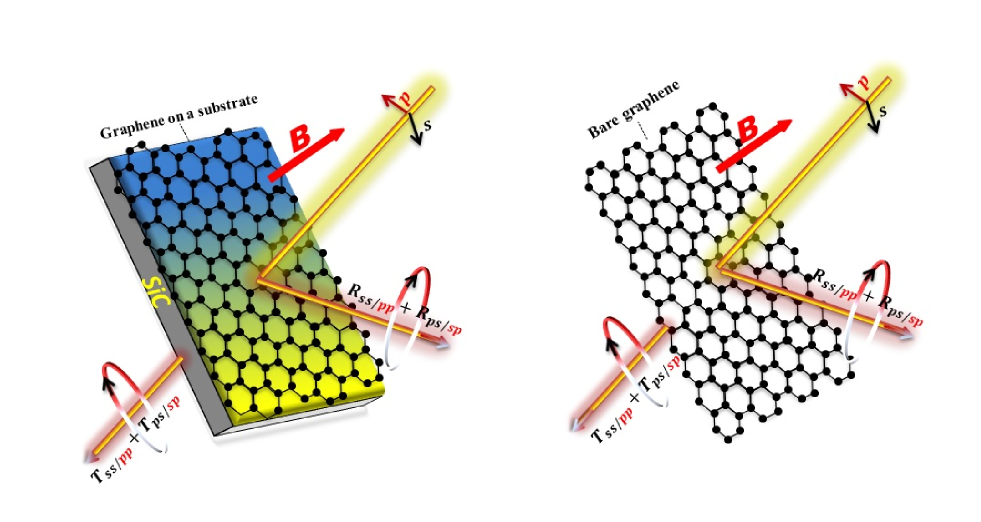
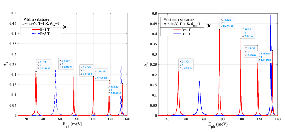
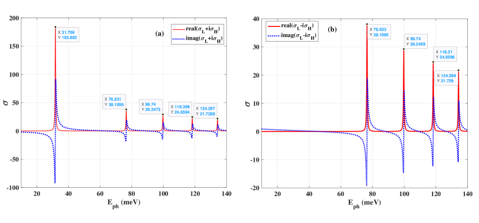
Our absorber structure is just based on a single-layer graphene under quantum Hall effect situation. However, as a matter of more illustration we also consider graphene layer to be on a dielectric substrate as it is demonstrated schematically in Fig.1. Here, the dielectric substrate is considered to be (with the dielectric constant ) on which graphene could be epitaxially grown with a controlled number of atomic layer []. First, in our simulations, we consider the incoming TE polarization (s-polarized) to obtain the absorption performance of graphene in a relatively low magnetic field for the proposed structure. We show the results in an energy interval ranging from to for the chemical potential and Faraday geometry in which the external magnetic field is perpendicular to surface of graphene, i.e. along the propagation of incoming linearly polarized light (the case ). It is clear from Fig.2 that graphene in the magnetic fields reveals a multi-band absorption performance. When the magnetic field is set to be and , the absorption of a graphene layer in the presence of a substrate has the amount of about and corresponding to the and photon energy, respectively. However, for bare graphene layer the absorption ratio is and for and , respectively. Now, if we take attention to the effective optical conductivity of graphene for the same parameters and , we see that boosting in absorption is directly related to the nature of the optical conductivity of graphene. In Fig. 3, We show the real and imaginary parts of the effective optical conductivity of graphene. As it is seen, each absorption peaks (for graphene with and without a substrate) in the energy position, exactly corresponding to the peaks of the optical conductivity of graphene. Consequently, this result indicates that the absorption performance of bare graphene could be tuned by modifying its optical conductivity.
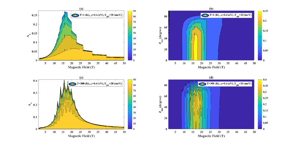
The absorption of single-layer graphene under an increasing applying magnetic field for different angles of the incoming light for and at a very low temperature and the room temperature is depicted in Fig. 4. We, in Fig. 4 (a), observe a step-like scheme emerges for the absorption of graphene as a function of the magnetic field ranging from to . It is clear that by increasing the magnetic field the absorption is also increased until it reaches its ultimate amount. Then this trend is reversed and the absorption falls gradually by increasing the field. In Fig. 4 (b) the role of scattering angle in the absorbtion is more clear. Note that, as it is clear from Fig. 4 (c) at a higher temperature the absorption will be boosted to some extend and the step-like scheme tends to vanish. The situation is more illustrated in Fig.4 (d).
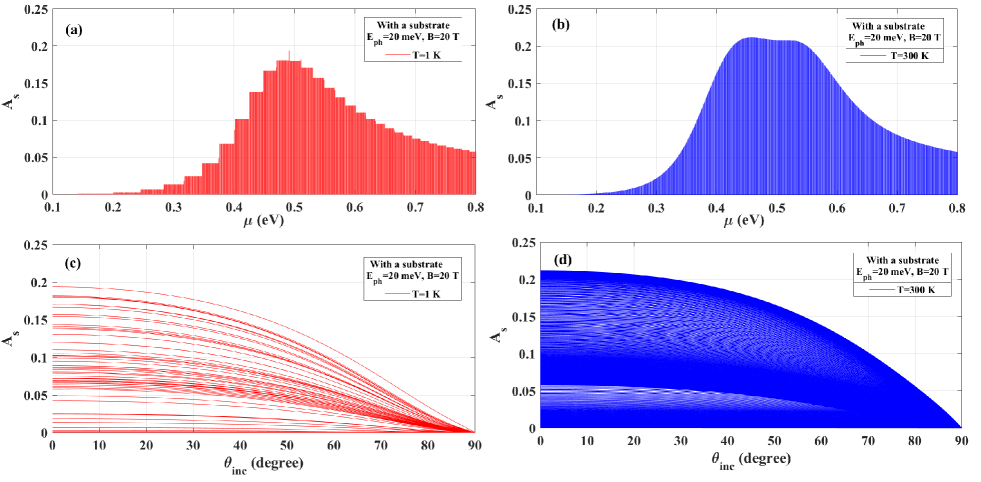
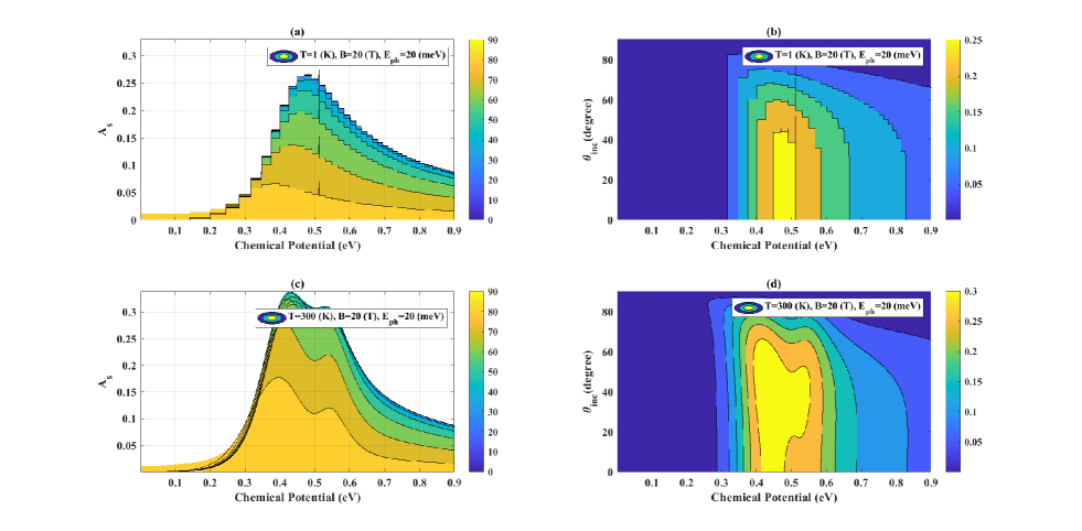
In the following, the effect of the chemical potential ranging from to on the absorption performance on graphene has been surveyed. The outcomes are illustrated as a function of the angle of the incidence of incoming linearly polarized light and also two different temperatures. For graphene with a substrate ( and ) similar to the magnetic field case, a plateau-like shape for the absorption can be seen (Fig. 5 (a)). The absorption is increased step by step until about , then it begins to fall. Note that, in spite of the fact that the highest plateau has happened in the chemical potential between and , the maximum absorption is occurred at with at . From Fig. 5(c) it is clear that enlarging angle of the incoming light leads to the lower absorption for graphene. Besides, at high temperatures, the absorption rate is boosted up to and the step-like structure, as it might be expected, also tends to be faded. In Fig. 6, the absorbtion versus the chemical potential for graphene without a substrate in a similar condition as indicated in Fig. 5, have been examined. In comparison to Fig. 5, the step-like situation is also taking place and the absorption is increased by increasing the chemical potential.
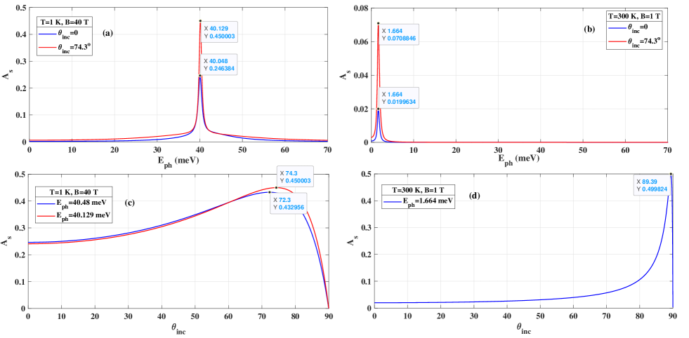
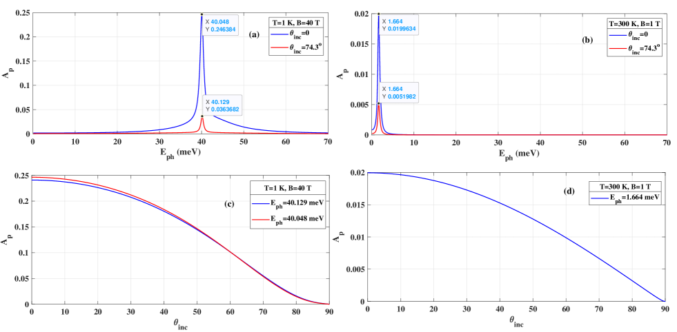
At this point, to see how the photon energy () ranging from to affects the absorption of graphene, we also examine it as a function of the incident angles at and for and . For graphene layer as it is observed from Fig. 7(a), the absorption of incoming s-polarized light shows a peak at a specific angle. Therefore, we see that increases when the direction of the applied magnetic field makes an angle to the propagation of the incident light relative to the Faraday geometry for a specific light’s scattering angle. However, the absorption of the incoming p-polarized incident light increasing by increasing the scattering angle leads to lower values for (see Fig. 8).
4 Conclusion
In summery, we investigated the absorbtion spectrum of intraband and interband transitions through the surface conductivity tensor of graphene in its general anisotropic state. We have numerically detailed the optical absorption of single layer graphene in THz region with and without a substrate () under quantum Hall effect situation. Since, in general, the initial polarization of light will no be preserved under the presence of the magnetic field, we have examined the effect of increasing the static magnetic field, chemical potential and photon energy interval for different incident angles of the incoming linearly polarized light. It was shown that any peak in the absorption performance of graphene layer in the photon energy interval directly corresponds to the enhancement of the optical conductivity of monolayer graphene. Therefore, we see that enhancement of the absorbtion of bare graphene is directly related to the profile of the optical conductivity of graphene. However, one can use photonic resonates and other resonance methods to increase the absorbtion of graphene-based devices. Significantly, applying a magnetic field on garpehene results in appearing a step-like scheme in the absorbtion of graphene at low temperatures. Moreover, we proved that higher absorbtion for bare graphene can be achieved for special incident angles of incident light relative to the Faraday geometry which may open opportunities for further investigation of light absorbtion in graphene-based THz application.
5 Data availability
Data sharing is not applicable to this article as no new data were created or analyzed in this study.
References
- [1] J. Lloyd-Hughes, J. Faist, H. E. Beere, D. A. Ritchie, L. Sirbu, I. M. Tiginyanu, S. K. M. Merchant and M. B. Johnston. Terahertz conductivity of magnetoexcitons and electrons in semiconductor nanostructures. Ultrafast Phenomena in Semiconductors and Nanostructure Materials XIII. Vol. 7214. SPIE, 2009.
- [2] J. Federici, L. Moeller. Review of terahertz and subterahertz wireless communications, J. Appl. Phys. 107 (11) (2010) 6 (2010).
- [3] P.U. Jepsen, D.G. Cooke, M. Koch, Terahertz spectroscopy and imaging-Modern techniques and applications, Laser Photon. Rev. 5 (1) 124-166 (2011).
- [4] Z. Wei, Y. Jiang, S. Zhang, X. Zhu, and Q. Li. Graphene-Based Magnetically Tunable Broadband Terahertz Absorber. IEEE Photonics Journal, 14(1), 1-6 (2021).
- [5] M. Tonouchi. Cutting-edge terahertz technology. Nature photonics, 1(2), 97-105 (2007).
- [6] J. Zhang, S. Cao, and L. Guan. Carbon monoxide gas sensor based on cavity enhanced absorption spectroscopy and harmonic detection. 2009 Symposium on Photonics and Optoelectronics (pp. 1-4). IEEE.
- [7] C. M. Watts, X. Liu, and W. J. Padilla. Metamaterial electromagnetic wave absorbers (adv. mater. 23/2012). Advanced Materials, 24(23), OP181-OP181 (2012).
- [8] ….B. Sensale-Rodriguez, R. Yan, M. M. Kelly, T. Fang, K. Tahy, W. S. Hwang, D. Jena, L. Liu and H. G. Xing. Broadband graphene terahertz modulators enabled by intraband transitions. Nature communications, 3(1), 1-7 (2012).
- [9] A. C. Neto, F. Guinea, N.M. Peres, K.S. Novoselov, A.K. Geim, The electronic properties of graphene, Rev. Modern Phys. 81 (1)109 (2009).
- [10] A. K. Geim, K.S. Novoselov, The rise of graphene. Nat. Mater, 6(3), 183-191 (2007).
- [11] L. A. Falkovsky. Optical properties of graphene. ournal of Physics: conference series. Vol. 129. No. 1. IOP Publishing, (2008).
- [12] H. Yang, Y. Wang, Z. C. Tiu, S. J. Tan, L. Yuan, and H. Zhang. All-Optical Modulation Technology Based on 2D Layered Materials. Micromachines, 13(1), 92 (2022).
- [13] C. C. Lee, S. Suzuki, W. Xie, and T. R. Schibli. Broadband graphene electro-optic modulators with sub-wavelength thickness. Optics express, 20(5), 5264-5269 (2012).
- [14] H. Yang, Y. Wang, Z. C. Tiu, S. J. Tan, L. Yuan, and H. Zhang. All-Optical Modulation Technology Based on 2D Layered Materials. Micromachines, 13(1), 92 (2022).
- [15] A. Nematpour, N. Lisi, L. Lancellotti, R. Chierchia, and M. L. Grilli. Experimental Mid-Infrared Absorption of Single-Layer Graphene in a Reflective Asymmetric Fabry-Perot Filter: Implications for Photodetectors. ACS Applied Nano Materials, 4(2), 1495-1502 (2021).
- [16] M. Grande, M. A. Vincenti, T. Stomeo, G. V. Bianco, D. De Ceglia, N. Akozbek, V. Petruzzelli, G. Bruno, M. De Vittorio, M. Scalora, and A. D’Orazio. Graphene-based perfect optical absorbers harnessing guided mode resonances. Optics Express, 23(16), 21032-21042 (2015).
- [17] R. R. Nair, P. Blake, A. N. Grigorenko, K. S. Novoselov, T. J. Booth, T. Stauber, N. M. R. Peres, and A. K. Geim. Fine structure constant defines visual transparency of graphene. Science, 320(5881), 1308-1308 (2008).
- [18] J. M. Dawlaty, S. Shivaraman, J. Strait, P. George, M. Chandrashekhar, F. Rana, M. G. Spencer1, D. Veksler, and Y. Chen. Measurement of the optical absorption spectra of epitaxial graphene from terahertz to visible. Applied Physics Letters, 93(13), 131905 (2008).
- [19] S. Cao, Q. Wang, X. Gao, S. Zhang, R. Hong, and D. Zhang. Monolayer-Graphene-Based Tunable Absorber in the Near-Infrared. Micromachines, 12(11), 1320 (2021)..
- [20] S. Lee, H. Heo, and S. Kim. Graphene perfect absorber of ultra-wide bandwidth based on wavelength-insensitive phase matching in prism coupling. Scientific reports, 9(1), 1-9 (2019).
- [21] B. Liu, C. Tang, J. Chen, N. Xie, H. Tang, X. Zhu, and G. S. Park. Multiband and broadband absorption enhancement of monolayer graphene at optical frequencies from multiple magnetic dipole resonances in metamaterials. Nanoscale research letters, 13(1), 1-7 (2018)
- [22] Z. Wu, B. Xu, M. Yan, B. Wu, Z. Sun, P. Cheng, X. Tong, and S. Ruan. Broadband microwave absorber with a double-split ring structure. Plasmonics, 15, 1863-1867 (2020).
- [23] H. S. Lee, J. Y. Kwak, T. Y. Seong, G. W. Hwang, W. M. Kim, I. Kim, and K. S. Lee. Optimization of tunable guided-mode resonance filter based on refractive index modulation of graphene. Scientific reports, 9(1), 1-11 (2019).
- [24] J. D. Joannopoulos, S. G. Johnson, J. N. Winn, and R. D. Meade. Molding the flow of light. Princeton Univ. Press, Princeton, NJ [ua] (2008).
- [25] X. Wang, X. Jiang, Q. You, J. Guo, X. Dai, and Y. Xiang, Y. Tunable and multichannel terahertz perfect absorber due to Tamm surface plasmons with graphene. Photonics Research, 5(6), 536-542 (2017).
- [26] Aperiodic perforated graphene in optical nanocavity absorbers, S Bidmeshkipour, OAkhavan, P Salami, L Yousefi, Materials Science and Engineering: B 276 115557 (2022).
- [27] Bidmeshkipour, Samina, and Omid Akhavan. ”Graphene Nanopores in Broadband Wide-Angle Optical Cavity Resonance Absorbers.” Surfaces and Interfaces (2022): 101956.
- [28] S. Lee, and S. Kim. ”Practical perfect absorption in monolayer graphene by prism coupling.” IEEE Photonics Journal 9.5: 1-10 (2017).
- [29] Q. Ye, J. Wang, Z. Liu, Z. C. Deng, X. T. Kong, F. Xing, X. D. Chen, W. Y. Zhou, C. P. Zhang, and J. G. Tian. Polarization-dependent optical absorption of graphene under total internal reflection. Applied Physics Letters, 102(2), 021912 (2013).
- [30] T. Okamoto, M. Yamamoto, and I. Yamaguchi, (2000). Optical waveguide absorption sensor using a single coupling prism. JOSA A, 17(10), 1880-1886.
- [31] H. Li, L. Wang, and X. Zhai. Tunable graphene-based mid-infrared plasmonic wide-angle narrowband perfect absorber. Scientific reports, 6(1), 1-8 (2016).
- [32] M. Wang, Y. Wang, M. Pu, C. Hu, X. Wu, Z. Zhao, and X. Luo, X. Circular dichroism of graphene-based absorber in static magnetic field. Journal of Applied Physics, 115(15), 154312 (2014).
- [33] M. Born and E. Wolf, Principles of Optics, 6th ed. (Cambridge University Press, Cambridge, 1980).
- [34] V. P. Gusynin, S. G., Sharapov, and J. P. Carbotte. Magneto-optical conductivity in graphene. Journal of Physics: Condensed Matter, 19(2), 026222 (2006).