Zn2GeO4/SnO2 nanowire architecture: A correlative spatially resolved X-ray study
Abstract
Wide bandgap semiconductor heterostructures based on nanowires have attracted great interest as one of the nanoscale building blocks for the development of novel optoelectronic devices. Owing to the critical role of heterogeneities and structural imperfections in the optoelectronic properties, it has become a challenge to investigate in detail the local structure and elemental composition of these systems. Typically, transmission electron microscopy and energy dispersive X-ray spectroscopy are applied to address such issues. Here, using a synchrotron nanobeam probe, we show a correlative spatially-resolved study of the composition, luminescence and local structure of a Zn2GeO4/SnO2 nanowire-based system. Unlike other works, the heterostructures were synthesized by an effective catalyst-free thermal evaporation method and present a skewer-shaped architecture formed by Plateau-Rayleigh instability. Our results highlight the role of diffused impurities on the optical properties of the heterostructure and open new avenues for further heterogeneity studies using the X-ray nanoprobe.
keywords:
X-ray nanoprobe, nanowire-heterostructures, Plateau− Rayleigh instability, wide bandgap oxides, XRF, XEOL, XASDepartamento de Física de Materiales, Facultad de Ciencias Físicas, Universidad Complutense de Madrid, 28040-Madrid, Spain \alsoaffiliationInstituto de Ciencia de Materiales de Madrid, Consejo Superior de Investigaciones Científicas, 28049 Cantoblanco, Spain
![[Uncaptioned image]](/html/2206.09730/assets/ToC.png)
Zn2GeO4/SnO2 nanowire architecture: A correlative spatially resolved X-ray study
Jaime Dolado, Fernanda Malato, Jaime Segura-Ruiz, María Taeño, Irina Snigireva, Pedro Hidalgo, Bianchi Méndez, and Gema Martínez-Criado
Synopsis
Herein we present results on a correlative hard X-ray study of Zn2GeO4/SnO2 nanowire heterostructures formed by Plateau-Rayleigh instability. The multi-technique synchrotron approach allows unraveling the elemental composition, optical processes and short-range order, making it possible to determine them independently and spatially resolved at the nanometer length scale. This study highlight the role of diffused impurities on the optical properties of nano-heterostructures and open new avenues for further heterogeneity studies using the X-ray nanoprobe.
Nanowires represent key building blocks for high density device-based nanotechnology. They are critical elements to implement the “bottom-up” approach to nanoscale fabrication, whereby well-defined nanosized architectures with unique physical properties are assembled into electronic and photonic devices. Moreover, by manipulating growth kinetics it is possible today to create more complex nanoscale heterostructures. The introduction of sequential branching, for example, with variations in the composition and/or doping will make possible novel electronic and photonic functionality into these building blocks1, 2, 3. Likewise, owing to the Plateau-Rayleigh (PR) instability, for example, Zn2GeO4/SnO2 heterostructures with skewer-like (SK) morphologies have been recently synthesized4, emerging as direct competitors to traditional wide bandgap materials for ultraviolet optoelectronic nanodevices. Thus, elongated Zn2GeO4 nanorods (E 4.5 eV) decorated with a linear array of SnO2 crystals (E 3.6 eV) in a necklace fashion were made by an effective thermal evaporation method. Yet, the concept underlying these building blocks rests on controlling the structural and optical properties at the nanometer scale. Often, the oxide nano-heterostructures suffer from native defects, heterogeneities, and/or local structural imperfections that can drastically affect their optoelectronic response5, 6, 7. So far, the structural and compositional quality of these nanowire architectures has been mostly gauged by correlative transmission electron microscopy (TEM) and energy dispersive X-ray spectroscopy (EDS) measurements4, 8, 9, 10, 11. Additionally, indirect methods such as cathodoluminescence measurements have been also applied to determine local heterogeneities in these nanowire-based systems12, 13. However, the formation of the individual components of these decorated nanostructures also needs a systematic structural and chemical study at the nanometer scale. Although the creation of crystalline phases driven by PR mechanism has been demonstrated, so far there are many open questions. Just few examples include the role of impurities on coupling formation and local atomic site configuration14, how these necklace structures are joined to form decorated architectures15, 16, 17, whether there is a full control over composition, diffusion paths, and/or structural modifications18, 19, 20, coexisting structural polytypes21, 22, diffusion-driven effects23, phase separation problems24, radial or axial chemical modulations22, as well as atomic scale variability due to fluctuations in the growth rate4.
Consequently, apart from a few cases in which single crystal X-ray diffraction measurements of nanowires could be recorded25, 26, 27, almost no information about the crystal symmetry of individual nanostructures and their integration into single architectures is available. Some works have reported the first applications of nano-X-ray absorption spectroscopy to single nanowires28, 29, 30. Thus, if X-ray excited optical luminescence is added to an X-ray absorption experiment, the challenge of a correlative study of single nanostructures can be overcome using hard X-ray nanobeams. Therefore, here we address such issues by characterizing a representative Zn2GeO4/SnO2 nano-heterostructure formed by PR mechanism obtained in a one-step thermal evaporation method4.
In this work we illustrate the use of a hard X-ray nanoprobe to study decorated nanowire based architectures by multiple contrast mechanisms using the nano-analysis beamline ID16B of the European Synchrotron Radiation Facility (ESRF). Using a pair of Kirkpatrick-Baez Si mirrors, our study involves the collection of X-ray fluorescence (XRF) and X-ray excited optical luminescence (XEOL) emissions induced by a highly focused and intense hard X-ray nanobeam. Both XRF and XEOL signals were recorded simultaneously. Whereas the characteristics XRF is recorded with an energy dispersive Si drift detector (deadtimes below 20%) at an angle of = (15 ± 5)º with respect to the sample surface, the luminescence is detected normal to this surface by a far-field optical collection system31. We apply this experimental scheme to SK-structures composed by a Zn2GeO4 nanowires and tin oxide crystallites produced by an effective thermal evaporation method 4. Compared to most of the previous reports3, here we use a catalyst-free mechanism to form the wide bandgap heterostructures. The droplets created by the PR instability act as nucleation centres, giving rise to an unprecedented control over the surface morphology18, 15.
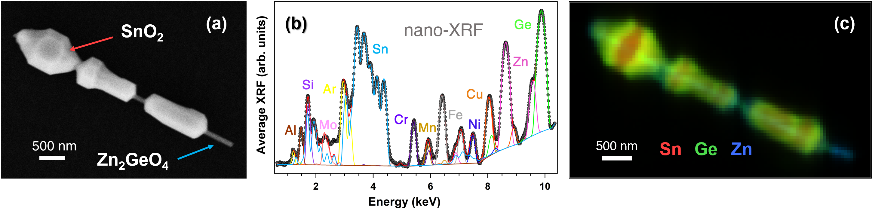
Figure 1a shows the scanning electron microscopy (SEM) image of a single Zn2GeO4/SnO2 nanoheterostructure taken with a LEO 1530 SEM equipment. It consists of a straight central wire surrounded by well-faceted crystallites (SK-like shape). The wire dimensions are 5 m length and 100 nm diameter, whereas the crystallites present sizes ranging between 500 - 800 nm. Figures 1b-c shows the X-ray nanoimaging results obtained by raster-scanning the SK-structure in the X-ray nanobeam. The monochromatic X-ray beam was focused to 80 x 60 nm2 spot size ( × ) with 1011 ph/s at room temperature in air. The XRF maps were taken at 11.25 keV (above the absorption edge of Ge located at 11.1031 keV) with a pixel size of 50 x 50 nm2 over a 3 × 5 m2 sample area with an integration time of 1000 ms per point. In addition to the major elements (Zn, Ge and Sn) of the Zn2GeO4/SnO2 heterostructure, the average XRF spectrum (Figure 1b) also reveals unintentional dopants (e.g., Cr, Fe, Ni and Cu) homogeneously distributed and likely originated from contaminants in precursors or in the reactor. Figure 1c shows Zn (blue), Ge (green) and Sn (red) superimposed distributions (individual elemental distribution maps can be seen in the Supporting Information). The composition of the nanowire axis is basically Zn2GeO4, as expected. However, the XRF maps of the SnO2 crystallites exhibit an interesting sandwich like pattern. A significant incorporation of Ge takes place within the SnO2 crystallites, which could modify the short-range order and give rise to secondary phases or defects, affecting accordingly the carrier recombination mechanisms. Moreover, an axial variation of the Sn localization is observed within the crystallites, being especially high in the fully faceted areas, whereas Ge is particularly distributed in the regions not completely faceted (see Supporting Information for further details). Finally, the Zn signal (Figure SI-2c in Supporting Information) comes mainly from the nanowire with a much lesser degree incorporated into the crystallites.
In good agreement with these results, we recently reported the observation of a high Ge fraction within the SnO2 crystallites (from 8% to 17%) by TEM-EDS. Our results point to the formation of a solid solution, such as Sn1-xGexO2, which keeps the rutile crystal structure4. Likely, the faceted areas present a lower amount of Ge (and a higher amount of Sn) because the Ge out-diffusion to the Zn2GeO4 nanowire surface (which is arranged in periodic droplets due to PR instability) acts as nucleation sites for the Sn crystals. The more faceted the crystal is, the more Sn replaced Ge to form the rutile crystal phase. Recent studies have shown that the nanowire coating in the PR-type processes is determined by parameters such as the evolution of the internal crystalline nanostructure over time, or the exchange of free atoms between the nanowire surface and the enveloping near-surface layer22, 21. Therefore, these factors could be involved in the different distribution of Ge and Sn in the SK-structure.
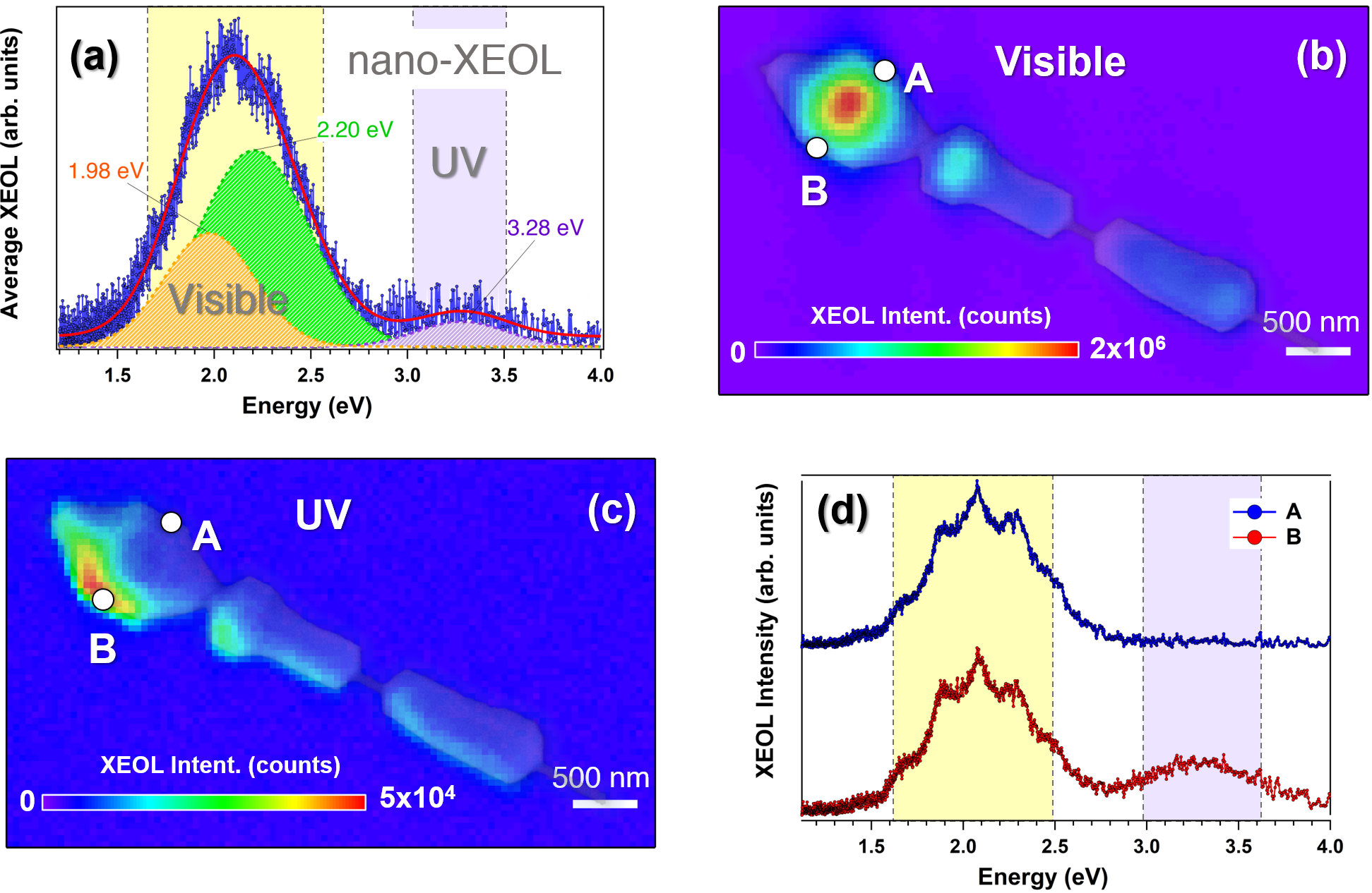
We have also exploited the optical contrast mechanism to record spectrally and spatially resolved XEOL signals simultaneously to XRF data for each point of the sample (see Figure 2). After the primary X-ray absorption process, most of the photogenerated electrons and holes recombine radiatively via secondary XRF and XEOL pathways. Figure 2a presents the average XEOL spectrum, where a main emission dominates in the visible range, and consists of two components located at 1.98 and 2.20 eV (indicated in orange and green colours, respectively). In addition, there is a weak band in the UV range located at 3.28 eV. The main observed band in the average XEOL spectrum corresponds to the emission related to the transition of the trapped electrons from oxygen vacancies to intrinsic surface states from the Sn1-xGexO2 crystallites. The luminescence of SnO2 is quite complex, exhibiting a broad emission band in the visible range, consisting of three components (orange, green and blue at 1.98, 2.25, and 2.58 eV, respectively) associated to oxygen vacancies32, 33. These components were also reported from SnO2 nanoribbons by XEOL measurements excited with both soft and hard X-rays34, 35. Regarding the weak UV band, this emission could come from the Zn2GeO4 nanowire, which exhibits a wide emission associated to oxygen vacancies in the UV range36. However, it has been observed that SnO2 nanorods and nanoparticles exhibited an UV emission related to surface states37, so it could also come from Sn1-xGexO2 particles.
Figures 2b and 2c display the spatial distribution of the respective XEOL bands. The visible emission associated to oxygen vacancies is radially distributed within the Sn1-xGexO2 crystallites, becoming particularly stronger from the well-faceted areas, where XRF signal of Sn is higher. Previously we observed that the crystallites of the SK-structures exhibit {110} facets4, in which the formation of oxygen vacancies would be easy since they are the planes of lower surface energy in SnO238. Therefore, this result suggests that the higher amount of Ge in some areas of the Sn1-xGexO2 particles would affect the amount of oxygen vacancies, with the consequent vanishing of the visible emission. On the other hand, the less intense UV emission of unclear origin is only present from one side of the Sn1-xGexO2 crystallites. The fact that the UV emission recorded in this work is only observed from one side of the Sn1-xGexO2 crystallite could suggest an orientation effect linked to the SnO2 crystal structure. Previous work have reported faceted dependent cathodoluminescence in SnO2 microtubes, which would imply different distribution of impurities and/or defects.32, 39 Alternatively, the UV emission could come from the preferential incorporation of defects arising from the out-diffusion of Ge or Zn from the Zn2GeO4 nanowire, which would result in new electronic states within the bandgap leading to the UV emission.
In order to spatially resolve at the nanoscale these luminescence related features with more details, Figure 2d shows the XEOL spectra acquired in two different points on the Sn1-xGexO2 crystallites (A and B). In both cases, the visible band related to SnO2 is the most pronounced contribution with some intensity modulation, resulting from the behaviour of the Sn1-xGexO2 crystallites as optical cavities4. On the other hand, the UV band is detected only from B, highlighting the inhomogeneous distribution of the radiative centres associated likely with the different distribution of impurities. As it is well known, the luminescence bands in semiconductors are related to the density of surface or defect electronic states37, 40.
In order to gain further information, given the heterogeneous nature of both composition and optical emissions, Figure 3 represents the normalized radial line profiles taken along the SK-structure (see Figure 3a). Figures 3 b, c and d show the XRF and XEOL profiles data obtained from each of the three Sn1-xGexO2 crystallites along the perpendicular direction to the central nanowire. For all cases, the Sn signal (in red colour) follows a similar trend according to the crystal volume with a maximum intensity at the centre of the Sn1-xGexO2 crystallites. The Ge signal (in green colour), on the other hand, presents a different profile for the largest crystal compared to the other two ones. The largest crystallite appears to be fully formed, producing a higher intensity from the edges of the structure. The smaller crystallites are conversely characterized by a more uniform Ge incorporation, with a Gaussian like profile according to their morphological shape. Finally, the Zn profiles (in blue colour) display a multipeak shape, indicating a pretty different and particular behaviour within the crystallite volume. The results not only reveal the incorporation of Zn within the Sn1-xGexO2 crystallites, but also its preferential spatial location towards the centre and edges of the crystallites.
Despite probing different sample depths (XEOL is much more surface sensitive than XRF), the radial line profiles of the XEOL signals provide complementary information about the three Sn1-xGexO2 crystallites. Compared to the XRF signal, the spatial distribution of XEOL is not only governed mainly by the beam spot size and penetration of the X-ray nanobeam within the sample (energy dependent, leading to a finite generation volume), but also greatly by the diffusion of the photogenerated carriers. Many factors can impact the resulting profile related to the sample itself in terms of sample morphology, composition, internal absorption and/or reflection mechanisms, as well as secondary photon emissions. The visible band profile (in orange) follows the crystal volume with a Gaussian like shape well correlated with Sn [with a smaller full width at half maximum (FWHM) due to diffusion effects]. The profile of the UV emission (in violet) presents a quite narrower line width peaking at the left edge of the Sn1-xGexO2 crystallite, matching one of the maxima in the Zn profile. The direct matching and interrelation between the UV band and Zn localization is also supported by axial line profiles recorded along the SK-structure (see Figure SI-3 in Supporting Information). It is important to emphasize that the UV emission is not observed in the bare Zn2GeO4 nanowire, ruling completely out their connection.
In short, the correlative study of the XRF and XEOL line profiles indicates that for the tin oxide crystallite fully formed (Figure 3b), likely there is an additional colocalization of Ge and Zn elements. On the other hand, for all the cases (Figure 3 b, c, d) the UV emission is in close relationship with the Zn distribution mainly concentrated at one of the edges of the Sn1-xGexO2 crystallites. This finding suggests that the UV emission could come from recombination centres linked to complexes associated to the presence of Zn.

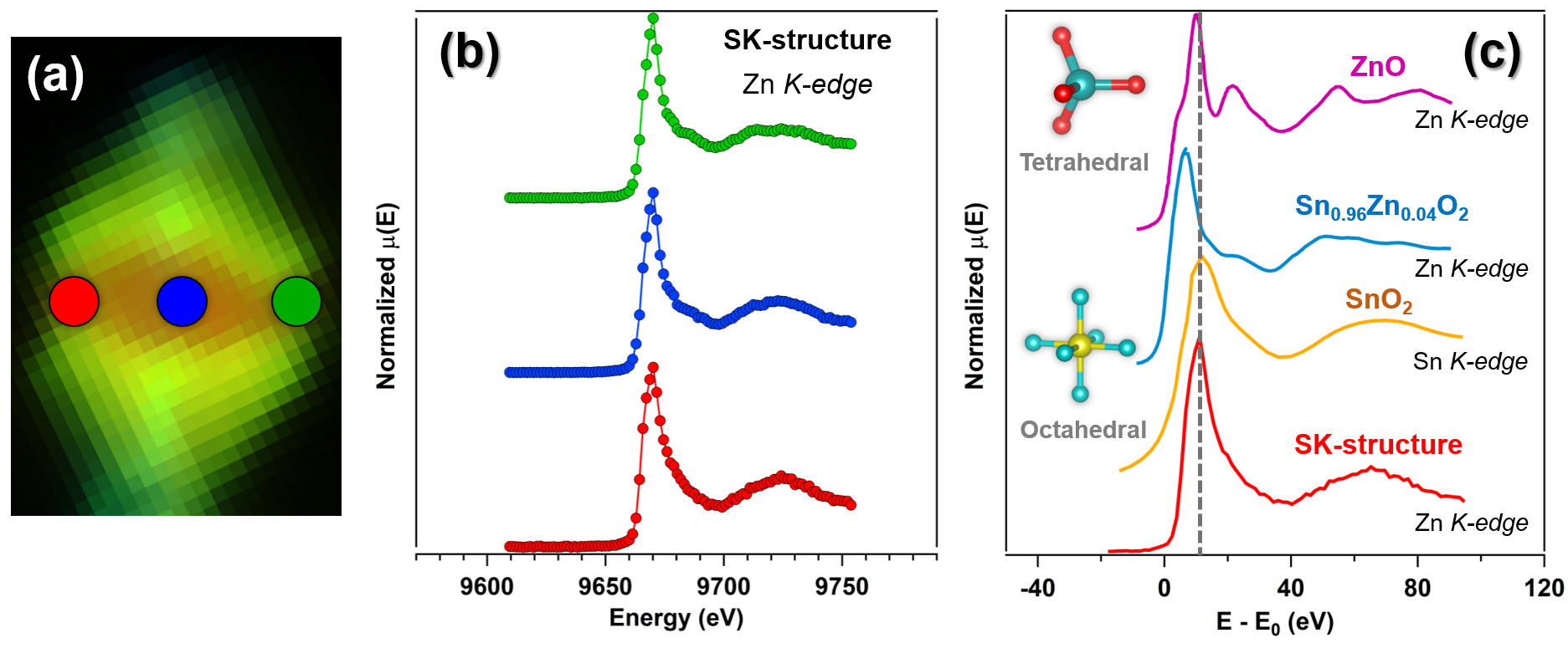
Given the key role of Zn within the Sn1-xGexO2 crystallites, in order to get a deeper insight into its local structure in the SK-structure, XANES data were taken around the Zn K-edge with nanometer spatial resolution. The measurements were performed with a beam size of 80 x 60 nm2 using a Si(111) double crystal monochromator with an energy resolution about 1 eV. Figure 4b shows the spatially resolved XANES data acquired in XRF detection mode over three different zones of the SK-structure. The XANES signal is analogous to the partial density of the empty states of the absorbing atoms; namely, to the energy band structure for crystalline material. In particular, XANES collected at the K edge reveals the -partial density of states in the conduction band. Here, two spectral XANES regions can be distinguished: a prominent white line assigned mainly to the 1 → 4 dipolar transitions, and the post-edge resonances, which are rather due to multiple scattering effects. The three XANES spectra collected on the Sn1-xGexO2 crystallite show an intense and narrow peak at 9670.2 eV, and the post-edge are similar in all three cases, indicating a similar short-range order around Zn atoms in the different areas.
An empirical and common practice is to assume that the XANES spectrum from an unknown local structural order can be understood as a linear superposition of the spectra of two or more known samples. Therefore, for comparison XANES spectra around the Zn or Sn K-edges of three model compounds are plotted in Figure 4c, in addition to one of those acquired from the Sn1-xGexO2 crystallites. In ZnO41, Zn atoms are in tetrahedral sites. In the Sn0.96Zn0.04O2 alloy, on the other hand, Zn is introduced into the SnO2 structure, inducing numerous lattice defects with no big change of the rutile crystal structure (octahedral environment)42. Finally, the XANES spectrum around Sn K-edge acquired on SnO2 with rutile structure is shown43, where each tin atom is expected to be coordinated by six oxygen atoms. Our results strongly suggest a substitutional Zn incorporation into the Sn sites. A direct comparison of XANES data from the post-edge region around the Zn and Sn K-edges for the Sn1-xGexO2 and SnO2, respectively, indicates the predominant octahedral coordination of Zn atoms in the Sn1-xGexO2 structure. In addition, theoretical XANES simulations of ZnO in a rutile-like environment show similar spectral shapes, corroborating our results44. Thus, the fact that the XANES spectrum of the Sn1-xGexO2 crystallites is significantly different from the XANES data of the Sn0.96Zn0.04O2 alloy suggests that Zn is incorporated as a dopant into the rutile structure, without causing major lattice distortions. In addition, the white line of the SK-structure is shifted to higher energies with respect to those of ZnO and the Sn0.96Zn0.04O2 alloy, indicating an increase in Zn coordination.
In short, XANES results point to Zn atoms in octahedral coordination within the Sn1-xGexO2 crystallites, indicating that it is being incorporated into the crystal lattice possibly as a dopant replacing Sn in the rutile structure. This substitutional Zn defect in the SnO2 lattice may lead to an electronic state within the gap responsible for the UV emission above observed by XEOL.
In summary, we showed the use of a hard X-ray nanoprobe with optical, elemental and local structure specificity for the study of Zn2GeO4/SnO2 heterostructures grown by an effective thermal evaporation method. Both the compositional and optical distributions were probed with nanometre resolution. Elemental maps showed that Ge and Zn atoms diffused from the central Zn2GeO4 nanowire to the Sn1-xGexO2 crystallite with an inhomogeneous character. On the other hand, XEOL maps revealed a homogeneous repartition of the dominant SnO2 related visible emission whereas the UV emission is only present on one side of the crystallite. A correlative study between XRF and XEOL line profiles allowed us to associate the presence of the UV band with a higher Zn concentration in certain areas of the Sn1-xGexO2 crystallite. XANES data collected in different areas of the crystallite around the Zn K-edge confirmed possible Zn octahedral coordination in the crystallites of the SK-structure. This finding could likely indicate the substitutional incorporation of Zn into the Sn sites in the rutile structure, leading to an electronic state within the bandgap responsible for the UV emission. Thus, this work shows how to complete the picture through correlative X-ray nano-analysis and how to develop wide bandgap nanowire-based architectures with bespoke properties at the nanoscale.
1 Associated content
Both distribution maps and normalized line profiles collected along the SK-structure from XRF and XEOL signals were processed with PyMca software.
This work has been supported by MICINN project RTI2018-097195-B-I00 and by European Union’s Horizon 2020 research and innovation programme under the Marie Skłodowska-Curie grant agreement n° 956548, project Quantimony. We thank the ESRF for the beam time allocated.
Vertical and horizontal X-ray beam profiles; Sn, Ge and Zn XRF maps of the SK-structure; and normalized XRF and XEOL line profiles collected along the SK-structure parallel to the central nanowire. This material is available free of charge.
References
- Lauhon et al. 2002 Lauhon, L. J.; Gudiksen, M. S.; Wang, D.; Lieber, C. M. Epitaxial core–shell and core–multishell nanowire heterostructures. nature 2002, 420, 57–61
- Lieber 2003 Lieber, C. M. Nanoscale science and technology: building a big future from small things. MRS bulletin 2003, 28, 486–491
- Jia et al. 2019 Jia, C.; Lin, Z.; Huang, Y.; Duan, X. Nanowire electronics: from nanoscale to macroscale. Chemical reviews 2019, 119, 9074–9135
- Dolado et al. 2019 Dolado, J.; Renforth, K. L.; Nunn, J. E.; Hindsmarsh, S. A.; Hidalgo, P.; Sánchez, A. M.; Méndez, B. Zn2GeO4/SnO2 Nanowire Heterostructures Driven by Plateau-Rayleigh Instability. Crystal Growth & Design 2019, 20, 506–513
- Dayeh et al. 2011 Dayeh, S. A.; Wang, J.; Li, N.; Huang, J. Y.; Gin, A. V.; Picraux, S. T. Growth, defect formation, and morphology control of germanium–silicon semiconductor nanowire heterostructures. Nano letters 2011, 11, 4200–4206
- Huijben et al. 2013 Huijben, M.; Koster, G.; Kruize, M. K.; Wenderich, S.; Verbeeck, J.; Bals, S.; Slooten, E.; Shi, B.; Molegraaf, H. J.; Kleibeuker, J. E., et al. Defect engineering in oxide heterostructures by enhanced oxygen surface exchange. Advanced functional materials 2013, 23, 5240–5248
- Li et al. 2016 Li, Y.; Huang, L.; Li, B.; Wang, X.; Zhou, Z.; Li, J.; Wei, Z. Co-nucleus 1D/2D heterostructures with Bi2S3 nanowire and MoS2 monolayer: One-step growth and defect-induced formation mechanism. ACS nano 2016, 10, 8938–8946
- Jung et al. 2007 Jung, Y.; Ko, D.-K.; Agarwal, R. Synthesis and structural characterization of single-crystalline branched nanowire heterostructures. Nano letters 2007, 7, 264–268
- Liu et al. 2008 Liu, Z.; Elbert, D.; Chien, C.-L.; Searson, P. C. FIB/TEM characterization of the composition and structure of core/shell Cu- Ni nanowires. Nano letters 2008, 8, 2166–2170
- Lim et al. 2009 Lim, S. K.; Brewster, M.; Qian, F.; Li, Y.; Lieber, C. M.; Gradecak, S. Direct correlation between structural and optical properties of III-V nitride nanowire heterostructures with nanoscale resolution. Nano letters 2009, 9, 3940–3944
- Gao et al. 2019 Gao, H.; Sun, W.; Sun, Q.; Tan, H. H.; Jagadish, C.; Zou, J. Compositional varied core–shell InGaP nanowires grown by metal–organic chemical vapor deposition. Nano letters 2019, 19, 3782–3788
- Hetzl et al. 2016 Hetzl, M.; Kraut, M.; Winnerl, J.; Francaviglia, L.; Döblinger, M.; Matich, S.; Fontcuberta i Morral, A.; Stutzmann, M. Strain-induced band gap engineering in selectively grown GaN–(Al, Ga)N core–shell nanowire heterostructures. Nano letters 2016, 16, 7098–7106
- Songmuang et al. 2016 Songmuang, R.; Giang, L. T. T.; Bleuse, J.; Den Hertog, M.; Niquet, Y.-M.; Dang, L. S.; Mariette, H. Determination of the optimal shell thickness for self-catalyzed GaAs/AlGaAs core–shell nanowires on silicon. Nano letters 2016, 16, 3426–3433
- Xu et al. 2018 Xu, S.; Li, P.; Lu, Y. In situ atomic-scale analysis of Rayleigh instability in ultrathin gold nanowires. Nano Research 2018, 11, 625–632
- Day et al. 2016 Day, R. W.; Mankin, M. N.; Lieber, C. M. Plateau–Rayleigh crystal growth of nanowire heterostructures: strain-modified surface chemistry and morphological control in one, two, and three dimensions. Nano letters 2016, 16, 2830–2836
- Li et al. 2017 Li, W.; Jia, Q.; Liu, X.; Zhang, J. Large scale synthesis and photoluminescence properties of necklace-like SiC/SiOx heterojunctions via a molten salt mediated vapor reaction technique. Ceramics International 2017, 43, 2950–2955
- Chu et al. 2018 Chu, Y.; Jing, S.; Yu, X.; Zhao, Y. High-temperature plateau–Rayleigh growth of beaded SiC/SiO2 nanochain heterostructures. Crystal Growth & Design 2018, 18, 2941–2947
- Day et al. 2015 Day, R. W.; Mankin, M. N.; Gao, R.; No, Y.-S.; Kim, S.-K.; Bell, D. C.; Park, H.-G.; Lieber, C. M. Plateau–Rayleigh crystal growth of periodic shells on one-dimensional substrates. Nature nanotechnology 2015, 10, 345–352
- Xue et al. 2016 Xue, Z.; Xu, M.; Zhao, Y.; Wang, J.; Jiang, X.; Yu, L.; Wang, J.; Xu, J.; Shi, Y.; Chen, K., et al. Engineering island-chain silicon nanowires via a droplet mediated Plateau-Rayleigh transformation. Nature communications 2016, 7, 1–9
- Liu et al. 2020 Liu, G.-S.; He, M.; Wang, T.; Wang, L.; He, Z.; Zhan, R.; Chen, L.; Chen, Y.; Yang, B.-R.; Luo, Y., et al. Optically Programmable Plateau–Rayleigh Instability for High-Resolution and Scalable Morphology Manipulation of Silver Nanowires for Flexible Optoelectronics. ACS Applied Materials & Interfaces 2020, 12, 53984–53993
- Gorshkov et al. 2020 Gorshkov, V. N.; Tereshchuk, V. V.; Sareh, P. Diversity of anisotropy effects in the breakup of metallic FCC nanowires into ordered nanodroplet chains. CrystEngComm 2020, 22, 2601–2611
- Walbert et al. 2020 Walbert, T.; Muench, F.; Yang, Y.; Kunz, U.; Xu, B.-X.; Ensinger, W.; Molina-Luna, L. In Situ Transmission Electron Microscopy Analysis of Thermally Decaying Polycrystalline Platinum Nanowires. ACS nano 2020, 14, 11309–11318
- Garín et al. 2017 Garín, M.; Jin, C.; Cardador, D.; Trifonov, T.; Alcubilla, R. Controlling Plateau-Rayleigh instabilities during the reorganization of silicon macropores in the Silicon Millefeuille process. Scientific reports 2017, 7, 1–11
- Allaire et al. 2021 Allaire, R. H.; Kondic, L.; Cummings, L. J.; Rack, P. D.; Fuentes-Cabrera, M. The role of phase separation on Rayleigh-Plateau type instabilities in alloys. The Journal of Physical Chemistry C 2021, 125, 5723–5731
- Bussone et al. 2015 Bussone, G.; Schäfer-Eberwein, H.; Dimakis, E.; Biermanns, A.; Carbone, D.; Tahraoui, A.; Geelhaar, L.; Haring Bolívar, P.; Schülli, T. U.; Pietsch, U. Correlation of electrical and structural properties of single as-grown GaAs nanowires on Si (111) substrates. Nano letters 2015, 15, 981–989
- Li et al. 2020 Li, N.; Labat, S.; Leake, S. J.; Dupraz, M.; Carnis, J.; Cornelius, T. W.; Beutier, G.; Verdier, M.; Favre-Nicolin, V.; Schülli, T. U., et al. Mapping Inversion Domain Boundaries along Single GaN Wires with Bragg Coherent X-Ray Imaging. ACS nano 2020, 14, 10305–10312
- Mostafavi Kashani et al. 2021 Mostafavi Kashani, S. M.; Dubrovskii, V. G.; Baumbach, T.; Pietsch, U. In situ monitoring of MBE growth of a single self-catalyzed GaAs nanowire by X-ray diffraction. The Journal of Physical Chemistry C 2021, 125, 22724–22732
- Segura-Ruiz et al. 2011 Segura-Ruiz, J.; Martinez-Criado, G.; Chu, M.; Geburt, S.; Ronning, C. Nano-X-ray absorption spectroscopy of single Co-implanted ZnO nanowires. Nano letters 2011, 11, 5322–5326
- Segura-Ruiz et al. 2014 Segura-Ruiz, J.; Martínez-Criado, G.; Denker, C.; Malindretos, J.; Rizzi, A. Phase Separation in Single InxGa1-xN Nanowires Revealed through a Hard X-ray Synchrotron Nanoprobe. Nano letters 2014, 14, 1300–1305
- Martínez-Criado et al. 2014 Martínez-Criado, G.; Segura-Ruiz, J.; Alén, B.; Eymery, J.; Rogalev, A.; Tucoulou, R.; Homs, A. Exploring Single Semiconductor Nanowires with a Multimodal Hard X-ray Nanoprobe. Advanced Materials 2014, 26, 7873–7879
- Martínez-Criado et al. 2016 Martínez-Criado, G.; Villanova, J.; Tucoulou, R.; Salomon, D.; Suuronen, J.-P.; Labouré, S.; Guilloud, C.; Valls, V.; Barrett, R.; Gagliardini, E., et al. ID16B: a hard X-ray nanoprobe beamline at the ESRF for nano-analysis. Journal of synchrotron radiation 2016, 23, 344–352
- Maestre et al. 2004 Maestre, D.; Cremades, A.; Piqueras, J. Cathodoluminescence of defects in sintered tin oxide. Journal of applied physics 2004, 95, 3027–3030
- Miller et al. 2017 Miller, D. R.; Williams, R. E.; Akbar, S. A.; Morris, P. A.; McComb, D. W. STEM-cathodoluminescence of SnO2 nanowires and powders. Sensors and Actuators B: Chemical 2017, 240, 193–203
- Zhou et al. 2006 Zhou, X.; Heigl, F.; Murphy, M.; Sham, T.; Regier, T.; Coulthard, I.; Blyth, R. Time-resolved X-ray excited optical luminescence from SnO2 nanoribbons: Direct evidence for the origin of the blue luminescence and the role of surface states. Applied physics letters 2006, 89, 213109
- Zhou et al. 2008 Zhou, X.; Zhou, J.; Murphy, M.; Ko, J.; Heigl, F.; Regier, T.; Blyth, R.; Sham, T. The effect of the surface of SnO2 nanoribbons on their luminescence using X-ray absorption and luminescence spectroscopy. The Journal of chemical physics 2008, 128, 144703
- Dolado et al. 2020 Dolado, J.; Hidalgo, P.; Méndez, B. The role of surface properties in the cathodoluminescence of Zn2GeO4/SnO2 nanowire heterostructures. Materials letters 2020, 275, 128152
- Kar et al. 2011 Kar, A.; Kundu, S.; Patra, A. Surface defect-related luminescence properties of SnO2 nanorods and nanoparticles. The Journal of Physical Chemistry C 2011, 115, 118–124
- Oviedo and Gillan 2000 Oviedo, J.; Gillan, M. Energetics and structure of stoichiometric SnO2 surfaces studied by first-principles calculations. Surface Science 2000, 463, 93–101
- Yuan et al. 2006 Yuan, X.; Lazzarini, L.; Salviati, G.; Zha, M.; Sekiguchi, T. Cathodoluminescence characterization of SnO2 nanoribbons grown by vapor transport technique. Materials science in semiconductor processing 2006, 9, 331–336
- Reshchikov and Morkoç 2005 Reshchikov, M. A.; Morkoç, H. Luminescence properties of defects in GaN. Journal of applied physics 2005, 97, 5–19
- Haug et al. 2011 Haug, J.; Chassé, A.; Dubiel, M.; Eisenschmidt, C.; Khalid, M.; Esquinazi, P. Characterization of lattice defects by X-ray absorption spectroscopy at the Zn K-edge in ferromagnetic, pure ZnO films. Journal of Applied Physics 2011, 110, 063507
- Liu et al. 2010 Liu, X.; Iqbal, J.; Wu, Z.; He, B.; Yu, R. Structure and room-temperature ferromagnetism of Zn-doped SnO2 nanorods prepared by solvothermal method. The Journal of Physical Chemistry C 2010, 114, 4790–4796
- Grandjean et al. 2004 Grandjean, D.; Benfield, R. E.; Nayral, C.; Maisonnat, A.; Chaudret, B. EXAFS and XANES study of a pure and Pd doped novel Sn/SnOx nanomaterial. The Journal of Physical Chemistry B 2004, 108, 8876–8887
- Zhu et al. 2014 Zhu, Q.; Ma, Q.; Buchholz, D.; Chang, R.; Bedzyk, M. J.; Mason, T. O. Structural and physical properties of transparent conducting, amorphous Zn-doped SnO2 films. Journal of Applied Physics 2014, 115, 033512