Magnetic imaging of superconducting qubit devices with scanning SQUID-on-tip
Abstract
We use a scanning superconducting quantum interference device (SQUID) to image the magnetic flux produced by a superconducting device designed for quantum computing. The nanometer-scale SQUID-on-tip probe reveals the flow of superconducting current through the circuit as well as the locations of trapped magnetic flux. In particular, maps of current flowing out of a flux-control line in the vicinity of a qubit show how these elements are coupled, providing insight on how to optimize qubit control.
Manufacturers of integrated circuits rely on a number of techniques to verify complex circuit designs, locate defects, and carry out failure analysis. These include optical microscopy, scanning electron microscopy, focused ion beam milling, microprobing, and thermal imaging, which – for example – is used to identify the location of short circuits via the Joule heating associated with large currents. Among non-destructive methods, imaging magnetic fields via scanning superconducting quantum interference device (SQUID) microscopy combines the highest spatial resolution with the highest current sensitivity [1, 2]. For these reasons, such scanning probes are particularly suited for the investigation of flux trapping and current flow in superconducting circuits [3, 4, 5, 6].
Here, we use a SQUID-on-tip probe [7, 8] to image a superconducting circuit designed for quantum computation. Maps of the stray magnetic field produced by the qubit control line in the vicinity of the transmon qubit reveal the details of the coupling, and may provide a route towards optimization of the device. Such maps can be reconstructed into images of current flow, which may be useful for the suppression of crosstalk originating from uncontrolled return current paths, i.e. currents draining from a qubit control line spuriously coupling flux to other qubits. Quantifying and mitigating such crosstalk is particularly relevant for the parallel execution of flux-controlled two-qubit gates [9, 10].
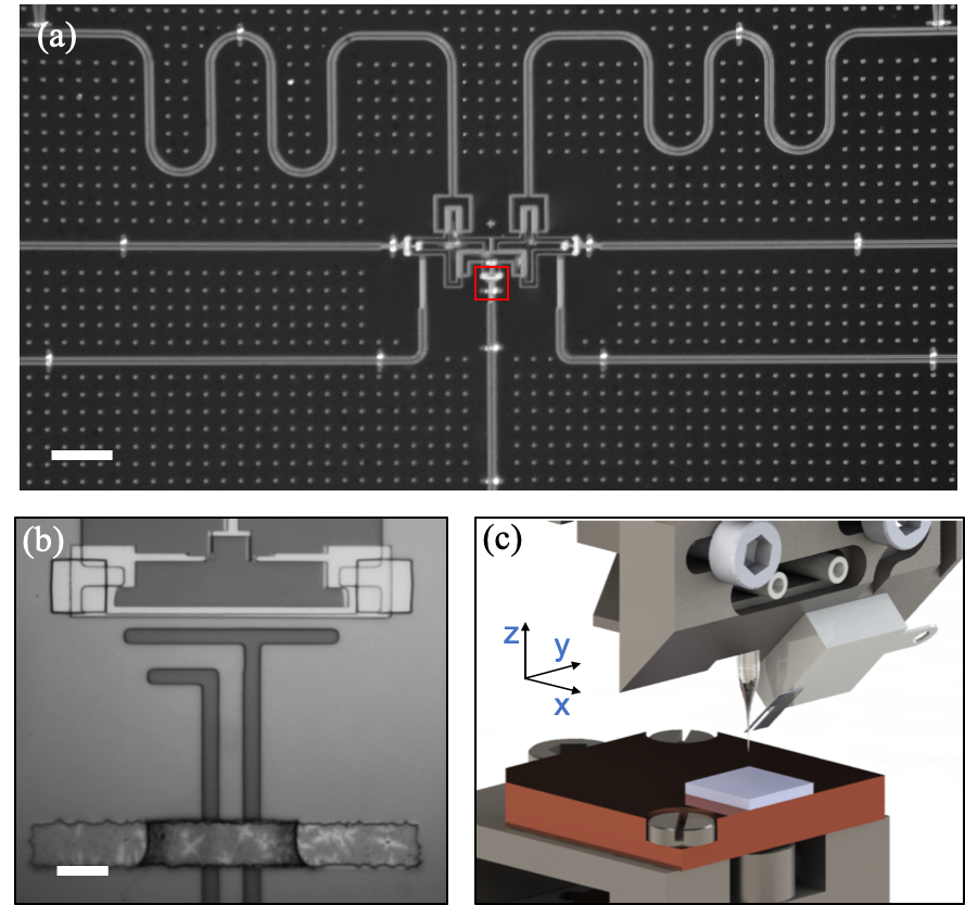
The superconducting qubit circuit that we investigate, is patterned from a 150-nm-thick Nb film deposited on a high-resistivity intrinsic Si substrate. Al airbridges are added to the device to establish a well connected ground plane. The circuit consists of three transmon qubits, each with flux-control lines, where the middle qubit is used as a tunable coupler [12]. The transmon qubits and the control line to which they are coupled are shown in the optical micrograph of Fig. 1 (a). We focus on the roughly region at the end of the central control line, shown in Fig. 1 (b), where the flux it produces couples to the SQUID loop of the transmon qubit above. The SQUID loop of the transmon qubit is made from Al and comprises two Josephson junctions whose electrodes are fabricated to form a closed loop and overlap with the Nb ground plane. In addition, electrical DC contact between the Al SQUID electrodes and the Nb ground plane is established using Al bandages [13].
In order to map the stray magnetic field perpendicular to the plane of the superconducting circuit, we carry out scanning SQUID microscopy (SSM) with a SQUID-on-tip probe mounted in a high-vacuum microscope operating at , shown schematically in Fig. 1 (c). The probe is fabricated by evaporating Pb on the apex of a pulled quartz capillary according to a self-aligned method pioneered by Finkler et al. [7] and perfected by Vasyukov et al. [8] The SQUID-on-tip used here has an effective loop-diameter of , as extracted from measurements of the critical current as a function of a uniform magnetic field , applied perpendicular to the SQUID loop.
The superconducting qubit circuit is mounted in the SSM in a plane parallel to and just below the loop of SQUID-on-tip, as shown in Fig. 1 (c). Since the current response of the SQUID-on-tip is proportional to the magnetic flux threading through its SQUID loop, it provides a measure of the component of the local magnetic field perpendicular to the circuit plane , integrated over the loop. A serial SQUID array amplifier (Magnicon) is used to measure the current flowing through the SQUID-on-tip [6]. The sample is positioned using piezoelectric positioners and scanners (Attocube). By scanning the sample at constant tip-sample spacing, we map with sub-micron spatial resolution that is limited by this spacing and – ultimately – by the SQUID-on-tip diameter.
In general, a map of magnetic field cannot be reconstructed into a map of its source current density by simply inverting the Biot-Savart law, because three-dimensional current densities do not produce unique magnetic field patterns. In-plane current densities or current densities in thick films that are uniform throughout their thickness, however, can be uniquely determined by their magnetic field. Therefore, by assuming a uniform current density along the thickness of the superconducting Nb film, which is of the order of its penetration depth, we can reconstruct from the measured [14, 15, 16].
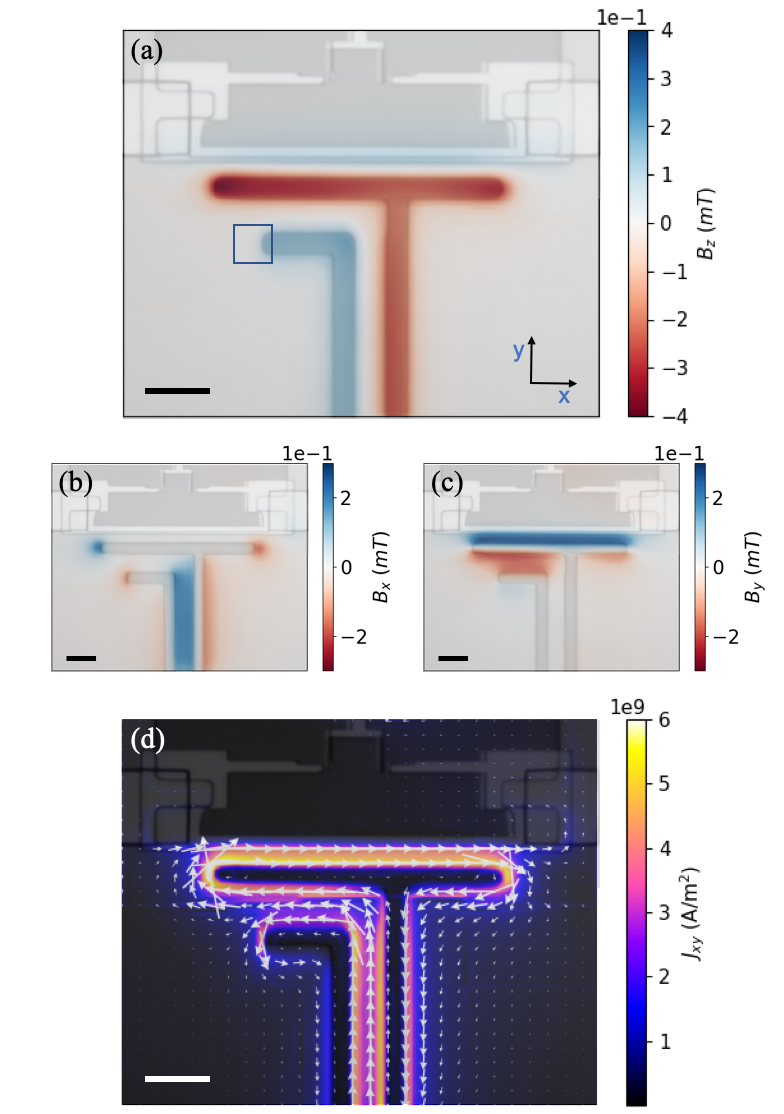
Fig. 2 (a) shows a map of AC , produced by of current at applied to the flux-control line and measured above the qubit circuit. The out-of-plane field vanishes above the superconducting Nb, due to the Meissner effect, and is concentrated in the gaps of exposed dielectric around the superconducting control line. Out-of-plane field is also measured in the bottom part of the transmon qubit’s SQUID loop, as well as over the Al film defining the bottom of the SQUID loop. At the measurement temperature of , unlike during normal operation of the qubit at , Al is not superconducting and therefore does not expel magnetic field. The in-plane components and , shown in Fig. 2 (b) and (c), can be calculated from the measured in the source-free region above the circuit, for slowly varying magnetic fields (in the magnetostatic limit) [17].
The reconstructed is plotted as a vector field in Fig. 2 (d), showing the flow of current out of the flux control line and into the ground plane. The flow pattern reveals how current density is concentrated along the edges of the Nb control line structures, as expected for a superconductor. As can be seen in the map of in Fig. 2 (a), the magnetic flux coupling into the SQUID loop of the transmon qubit, appearing as light blue contrast in the upper part, results principally from the return current flowing in the -direction, along the top edge, where the ground plane ends and the qubit structure begins. In particular, the narrowness of this superconducting channel, which provides the most direct connection between the two sides of the circuit’s ground plane, appears to concentrate the return current density in this region, enhancing the flux produced through the transmon structure. By integrating the current density, we find that of the flowing out of the control line flow through this narrow channel.
The coupling strength between the control line and the transmon can be quantified by a mutual inductance , where is the magnetic flux threading through the qubit’s SQUID loop and is the current flowing through the control line. By integrating the magnetic flux measured by our SSM in the region directly above the qubit’s SQUID, we estimate . This value is significantly larger than measured on another identical chip at via its flux periodicity as a function of DC current applied to the control line. This discrepancy is at least in part due to the difference in temperature between the two measurements, since none of the Al circuit elements, including the transmon SQUID loop itself or the airbridges, are superconducting at . As a result, return currents have different available superconducting paths along which to flow. Another possibile source of the discrepancy is the different configuration of the bonds at the edges of the chip connecting the ground plane to the system ground. The sample measured via SSM has fewer connections that are not uniformly distributed around the chip. Finally, although other SSM measurements were carried out in after zero-field cooling, the measurement shown in Fig. 2 was carried out in an applied field , because the SQUID-on-tip used in that case lacked sensitivity near zero field. At such fields, flux is expected to penetrate the ground plane, potentially affecting the flow of AC return currents.
For all of these reasons, this specific measurement should be taken as a demonstration showing that SQUID-on-tip SSM can provide detailed map of current flow in superconducting qubit circuits. However, if carried out below and on devices grounded as in normal operating conditions, maps of current density can give a precise picture of the desired and undesired inductive couplings. In addition, the uncertainty in determining mutual inductance in this measurement is due to both the limited accuracy in the alignment of the flux image measured via SSM with the geometry of the qubit and to the spread of the flux over the separating the plane of the qubit and the probe. Applying SSM probes that include simultaneous AFM measurements of sample topography, e.g. using probes developed by Wyss et al. [18] or done with smaller tip-sample separations would improve the measurement’s accuracy. Ultimately, SSM done as shown here can assist in the design of qubit circuits with increased mutual inductance. Increasing mutual inductance allows for the reduction in the size of the qubit SQUID loop and, in turn, a reduction in the flux noise due to ambient magnetic fields, making the qubit more robust. Given the ability of SQUID-on-tip sensors to detect a few tens of of current [8, 16], similar measurements could also identify current paths that lead to spurious coupling between a control line and other qubits on the chip. Identifying the sources of such cross-talk could aid in the design of circuits minimizing these effects.
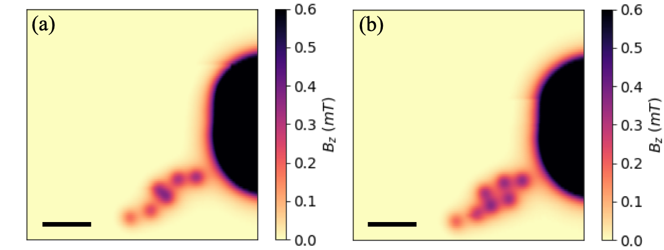
In addition to studying the flow of low-frequency current out of the qubit control lines, we also identify the locations where magnetic flux can be trapped in the circuit, when an external magnetic field is applied or a large DC current is sourced through the control lines. Fig. 3 (a) shows an image of the DC above the circuit after zero-field cooling followed by the application of an out-of-plane field . Dark regions represent regions of high magnetic field, where flux penetrates, while light regions represent vanishing magnetic field, due to the Meissner effect of the superconducting Nb film. corresponds to the lowest applied field, at which flux penetrates in the form of superconducting vortices, as seen in the lower half of Fig. 3 (a). In the investigated region, vortices are always seen to penetrate near the rounded edge of the flux control line. Both circuit geometry and defects in the Nb film are likely to play a role in concentrating magnetic flux and determining the location of initial vortex entry.
The addition of a DC current of is then seen to shift the position of the vortices and to introduce an additional vortex, as shown in Fig. 3 (b). Also, two vortices which were initially closer than our spatial resolution are seen to separate slightly. The new vortex penetrates just to the right of the newly separated vortices. The fact that a DC current through the control line, which is similar in magnitude to that used during qubit operation, results in the perturbation of vortices and the nucleation of a new vortex supports the possibility that trapped flux may be responsible for some of the low-frequency noise observed in similar qubit devices [19].
Unstable vortex configurations could produce fluctuations in magnetic flux and therefore in qubit frequency, ultimately leading to qubit decoherence. In fact, the circuit under investigation includes flux-trapping holes, appearing as regularly spaced features in Fig. 1 (a), except in the region around the qubit, in order not to affect its flux controllability. Although under normal operation, such a superconducting circuit would be shielded from external applied magnetic fields, vortices could penetrate as a result of the magnetic flux produced by residual background fields due to slightly magnetic sample-mounting components. In addtion, the control currents, which flow through the flux control lines and are on the order of mA, may also result in the penetration of flux. On the other hand, we did not observe the entry of vortices in the same region at with DC currents of up to . Recent studies have also suggested that qubit instability is the result of two-level system fluctuators, rather than vortex instability [20, 21, 22, 23].
These experiments show the potential of SSM with a nanometer-scale probe to reveal the details of current flow and flux control-line coupling in superconducting qubit circuits. In the future, comparison of current density maps measured below with simulations could help improve circuit design, both to optimize couplings and to reduce unwanted cross-talk and interference between qubits. Extending the bandwidth of nanometer-scale SSM probes from the kHz frequency range, which is currently possible, to hundreds of MHz or GHz would be useful for visualizing currents and fields from qubit control pulses and mapping the high-frequency behavior of the circuit. The identification of vortex entry as a result of flux produced by large control currents also may explain instabilities observed in qubit devices. The identification of threshold control currents for vortex entry may help mitigate these effects.
Acknowledgements.
We thank Sascha Martin and his team in the machine workshop of the Physics Department at the University of Basel. We acknowledge the support of the Canton Aargau and the Swiss National Science Foundation via Project Grant No. 200020-159893, Sinergia Grant Nanoskyrmionics (Grant No. CRSII5-171003), and via a Director’s Reserve grant of the National Centre for Competence in Research Quantum Science and Technology (QSIT). S.K. acknowledges financial support from Fondation Jean-Jacques et Félicia Lopez-Loreta and the ETH Zurich Foundation.The data that support the findings of this study are available from the corresponding author upon reasonable request.
References
- Chatraphorn et al. [2000] S. Chatraphorn, E. F. Fleet, F. C. Wellstood, L. A. Knauss, and T. M. Eiles, “Scanning SQUID microscopy of integrated circuits,” Appl. Phys. Lett. 76, 2304–2306 (2000).
- Knauss et al. [2001] L. A. Knauss, A. B. Cawthorne, N. Lettsome, S. Kelly, S. Chatraphorn, E. F. Fleet, F. C. Wellstood, and W. E. Vanderlinde, “Scanning SQUID microscopy for current imaging,” Microelectronics Reliability 41, 1211–1229 (2001).
- Jeffery et al. [1995] M. Jeffery, T. Van Duzer, J. R. Kirtley, and M. B. Ketchen, “Magnetic imaging of moat-guarded superconducting electronic circuits,” Appl. Phys. Lett. 67, 1769–1771 (1995).
- Stan, Field, and Martinis [2004] G. Stan, S. B. Field, and J. M. Martinis, “Critical Field for Complete Vortex Expulsion from Narrow Superconducting Strips,” Physical Review Letters 92 (2004).
- Jelić et al. [2017] Ž. L. Jelić, A. Gurevich, A. V. Silhanek, E. O. Lachman, E. Zeldov, G. P. Mikitik, L. Embon, M. E. Huber, M. V. Milošević, Y. Anahory, and Y. Myasoedov, “Imaging of super-fast dynamics and flow instabilities of superconducting vortices,” Nature Communications 8, 85 (2017).
- Ceccarelli et al. [2019] L. Ceccarelli, D. Vasyukov, M. Wyss, G. Romagnoli, N. Rossi, L. Moser, and M. Poggio, “Imaging pinning and expulsion of individual superconducting vortices in amorphous MoSi thin films,” Phys. Rev. B 100, 104504 (2019).
- Finkler et al. [2010] A. Finkler, Y. Segev, Y. Myasoedov, M. L. Rappaport, L. Ne’eman, D. Vasyukov, E. Zeldov, M. E. Huber, J. Martin, and A. Yacoby, “Self-Aligned Nanoscale SQUID on a Tip,” Nano Lett. 10, 1046–1049 (2010).
- Vasyukov et al. [2013] D. Vasyukov, Y. Anahory, L. Embon, D. Halbertal, J. Cuppens, L. Neeman, A. Finkler, Y. Segev, Y. Myasoedov, M. L. Rappaport, M. E. Huber, and E. Zeldov, “A scanning superconducting quantum interference device with single electron spin sensitivity,” Nat Nano 8, 639–644 (2013).
- Arute et al. [2019] F. Arute, K. Arya, R. Babbush, D. Bacon, J. C. Bardin, R. Barends, R. Biswas, S. Boixo, F. G. S. L. Brandao, D. A. Buell, B. Burkett, Y. Chen, Z. Chen, B. Chiaro, R. Collins, W. Courtney, A. Dunsworth, E. Farhi, B. Foxen, A. Fowler, C. Gidney, M. Giustina, R. Graff, K. Guerin, S. Habegger, M. P. Harrigan, M. J. Hartmann, A. Ho, M. Hoffmann, T. Huang, T. S. Humble, S. V. Isakov, E. Jeffrey, Z. Jiang, D. Kafri, K. Kechedzhi, J. Kelly, P. V. Klimov, S. Knysh, A. Korotkov, F. Kostritsa, D. Landhuis, M. Lindmark, E. Lucero, D. Lyakh, S. Mandrà, J. R. McClean, M. McEwen, A. Megrant, X. Mi, K. Michielsen, M. Mohseni, J. Mutus, O. Naaman, M. Neeley, C. Neill, M. Y. Niu, E. Ostby, A. Petukhov, J. C. Platt, C. Quintana, E. G. Rieffel, P. Roushan, N. C. Rubin, D. Sank, K. J. Satzinger, V. Smelyanskiy, K. J. Sung, M. D. Trevithick, A. Vainsencher, B. Villalonga, T. White, Z. J. Yao, P. Yeh, A. Zalcman, H. Neven, and J. M. Martinis, “Quantum supremacy using a programmable superconducting processor,” Nature 574, 505–510 (2019).
- Krinner et al. [2022] S. Krinner, N. Lacroix, A. Remm, A. Di Paolo, E. Genois, C. Leroux, C. Hellings, S. Lazar, F. Swiadek, J. Herrmann, G. J. Norris, C. K. Andersen, M. Müller, A. Blais, C. Eichler, and A. Wallraff, “Realizing repeated quantum error correction in a distance-three surface code,” Nature 605, 669–674 (2022).
- Ceccarelli [2020] L. Ceccarelli, Scanning Probe Microscopy with SQUID-on-tip Sensor, Ph.d. thesis, University of Basel (2020).
- Collodo et al. [2020] M. C. Collodo, J. Herrmann, N. Lacroix, C. K. Andersen, A. Remm, S. Lazar, J.-C. Besse, T. Walter, A. Wallraff, and C. Eichler, “Implementation of Conditional Phase Gates Based on Tunable ZZ Interactions,” Phys. Rev. Lett. 125, 240502 (2020).
- Dunsworth et al. [2017] A. Dunsworth, A. Megrant, C. Quintana, Z. Chen, R. Barends, B. Burkett, B. Foxen, Y. Chen, B. Chiaro, A. Fowler, R. Graff, E. Jeffrey, J. Kelly, E. Lucero, J. Y. Mutus, M. Neeley, C. Neill, P. Roushan, D. Sank, A. Vainsencher, J. Wenner, T. C. White, and J. M. Martinis, “Characterization and reduction of capacitive loss induced by sub-micron Josephson junction fabrication in superconducting qubits,” Appl. Phys. Lett. 111, 022601 (2017).
- Roth, Sepulveda, and Wikswo [1989] B. J. Roth, N. G. Sepulveda, and J. P. Wikswo, “Using a magnetometer to image a two-dimensional current distribution,” Journal of Applied Physics 65, 361–372 (1989).
- Chang et al. [2017] K. Chang, A. Eichler, J. Rhensius, L. Lorenzelli, and C. L. Degen, “Nanoscale Imaging of Current Density with a Single-Spin Magnetometer,” Nano Lett. 17, 2367–2373 (2017).
- Marchiori et al. [2022] E. Marchiori, L. Ceccarelli, N. Rossi, L. Lorenzelli, C. L. Degen, and M. Poggio, “Nanoscale magnetic field imaging for 2D materials,” Nat Rev Phys 4, 49–60 (2022).
- Lima and Weiss [2009] E. A. Lima and B. P. Weiss, “Obtaining vector magnetic field maps from single-component measurements of geological samples,” J. Geophys. Res. 114, B06102 (2009).
- Wyss et al. [2022] M. Wyss, K. Bagani, D. Jetter, E. Marchiori, A. Vervelaki, B. Gross, J. Ridderbos, S. Gliga, C. Schönenberger, and M. Poggio, “Magnetic, Thermal, and Topographic Imaging with a Nanometer-Scale SQUID-On-Lever Scanning Probe,” Physical Review Applied 17, 034002 (2022).
- Nsanzineza and Plourde [2014] I. Nsanzineza and B. L. T. Plourde, “Trapping a Single Vortex and Reducing Quasiparticles in a Superconducting Resonator,” Phys. Rev. Lett. 113, 117002 (2014).
- Klimov et al. [2018] P. V. Klimov, J. Kelly, Z. Chen, M. Neeley, A. Megrant, B. Burkett, R. Barends, K. Arya, B. Chiaro, Y. Chen, A. Dunsworth, A. Fowler, B. Foxen, C. Gidney, M. Giustina, R. Graff, T. Huang, E. Jeffrey, E. Lucero, J. Y. Mutus, O. Naaman, C. Neill, C. Quintana, P. Roushan, D. Sank, A. Vainsencher, J. Wenner, T. C. White, S. Boixo, R. Babbush, V. N. Smelyanskiy, H. Neven, and J. M. Martinis, “Fluctuations of Energy-Relaxation Times in Superconducting Qubits,” Phys. Rev. Lett. 121, 090502 (2018).
- Schlör et al. [2019] S. Schlör, J. Lisenfeld, C. Müller, A. Bilmes, A. Schneider, D. P. Pappas, A. V. Ustinov, and M. Weides, “Correlating Decoherence in Transmon Qubits: Low Frequency Noise by Single Fluctuators,” Phys. Rev. Lett. 123, 190502 (2019).
- Burnett et al. [2019] J. J. Burnett, A. Bengtsson, M. Scigliuzzo, D. Niepce, M. Kudra, P. Delsing, and J. Bylander, “Decoherence benchmarking of superconducting qubits,” npj Quantum Inf 5, 1–8 (2019).
- Müller, Cole, and Lisenfeld [2019] C. Müller, J. H. Cole, and J. Lisenfeld, “Towards understanding two-level-systems in amorphous solids: Insights from quantum circuits,” Rep. Prog. Phys. 82, 124501 (2019).